Note: Descriptions are shown in the official language in which they were submitted.
CA 02452574 2003-12-30
WO 03/004981 PCT/US02/20775
EMISSION SPECTROMETER HAVING CHARGE
COUPLED DEVICE DETECTOR
Field of the Invention
[0001] The present invention relates generally to an
analyzer having a charge coupled device based emission
spectrometer for ultra-high purity gas analysis.
Background of the Invention
[0002] For many years, gaseous emission spectroscopy
has been used for the analysis of nitrogen in argon (see
e.g., U.S. Patent No. 3,032,654). A commonly used
emission source for this technique is a low-energy argon
plasma, also known as a silent electric discharge (SED).
This technology has improved over the years to lower the
limit-of-detection (LOD) to single digit parts-per-
billion (ppb) levels; for example, through the use of
electro-optical modulation (see, e.g., U.S. Patent No.
5,412,467). Further improvements in sample cell design,
electronics, and the microprocessor plat.Eorm have led to
the current generation of spectroscopic analyzers. The
current practice of using multiple detectors and optical
filters allows for the simultaneous analysis of multiple
impurities if suitable emission wavelengths can be found.
[0003] The block diagram in Figure 1A shows the
emission and detection systems utilized in connection
with early analyzers that perform conventional emission
spectroscopy. Similarly, Figure 1B is a block diagram
for a state-of-the-art analyzer design using electro-
optic modul'ation, as described in U.S. Patent No.
5,412,467. In both types of systems, a high voltage
transformer 1 powers a light source 2 containing a
gaseous sample to be analyzed. The gases are excited by
the voltage to produce optical emission lines (an
CA 02452574 2006-10-27
WO 2003/004981 PCT/US2002/020775
2
emission spectrum) characteristic of each gas (impurity)
in the sample. Narrow bandpass optical filters 3 isolate
the strongest emission line corresponding to each
impurity. Photomultipliers (PMTs) 5 convert the light
output from each impurity to a current which is amplified
by a frequency selective amplifier, either a fixed
amplifier 6a as in Figure 1A or a tuned amplifier 6b as
in Figure 1B, and readout 7. The conventional system
uses a chopper wheel 4 to interrupt (or modulate) the
light to the PMT. Whereas, the electro-optic modulation
system uses a frequency doubler 8 and variable frequency
oscillator 9 to modulate the light to the PMT.
[0004] To date, each generation of emission
spectrometer has shared a common detection scheme. The
emission line of the impurity of interest is isolated by
a narrow bandpass optical filter and converted to an
electrical signal through the use of a photomultiplier
tube. The PMT has been the detector of choice for
numerous applications in low light level spectroscopy due
to the inherent high electronic gain possible through the
use of the PMT. In addition to sensitivity, the PMT is
also rugged, reliable, low cost, and stable over long
periods of time. These are important attributes when
used in a continuous-use application, such as emission
spectroscopy. However, PMTs do pose several problems
when used as detectors for emission spectroscopy. PMTs
are comparatively large devices by today's standards,
particularly when several PMTs must be used in a single
analyzer. Although PMTs are low cost, the high-quality
narrow bandpass filters are not, especially when several
filters are needed. Moreover, the narrow bandpass
filters, which isolate the emission line of interest for
a given impurity, also prevent evaluation of the
CA 02452574 2006-10-27 --- --~
WO 2003/004981 PCT/US2002/020775
3
background light level at the wavelength chosen for
analysis.
[0005] The background light level at the impurity
emission wavelength of interest can change for a variety
of reasons, such as changes in temperature, sample gas
pressure, excitation conditions, or other impurities
entering the discharge. It is extremely difficult to
distinguish background light level shifts from a changing
concentration of the impurity of interest when only the
emission intensity at the wavelength of interest is
known. Shifts in background light level can result in
problems with long term baseline drift, nonlinear
calibration curves, and cross sensitivity to other
impurities. These are all serious problems when
attempting to perform impurity analysis on impurities
with measurements in the parts per billion.
[0006] Figure 2 illustrates the problem inherent in
using the PMT and optical filter approach. Figure 2
shows six emission spectra labeled A-F; that respectively
correspond to 86, 56, 38, 25, 9 and 0 ppb concentrations
of-moisture (water vapor) in an argon samgle gas. Each
spectrum shows the region of the ultraviolet (UV)
spectrum where both moisture and nitrogen have
characteristic emission lines. Note that the addition of
moisture causes a rise in the baseline light level,
particularly in the region of the spectrum (333-360nm)
where nitrogen characteristically emits. If a PMT and
optical filter are used, this increased light level could
be interpreted as coming from a nitrogen impurity,
resulting in an erroneously high concentration of
nitrogen being reported. However, if the baseline light
level shift is evaluated properly, the fact that no
nitrogen emission peak is present can be correctly
CA 02452574 2006-10-27
WO 2003/004981 PCT/US2002/020775
4
determined, and hence the nitrogen concentration is
actually zero. The same argument applies to baseline
shifts due to other factors, as mentioned above, which
show up as noise and drift in the analytical results if
not taken into account. Two approaches have been
proposed to address the problem of changing baseline
light level.
[0007] First, a separate PMT detector can be dedicated
to determining the baseline emission light level rather
than analyzing for an impurity. This is done by choosing
a narrow bandpass filter that isolates a wavelength
region of the sample gas emission spectrum close to, but
not including, the impurity emission lines of interest.
The analyzer then uses the ratio of the signal from the
PMT measuring the impurity emission and the signal from
the PMT monitoring the baseline. This approach
eliminates many of the problems of the baseline emission
light level. However, this technique is more complicated
and requires either an additional PMT and optical filter
or a reduction in the number of impurities which can be
detected.
[0008] In the second approach, the baseline drift and
some of the nonlinearity in the calibration curve of the
analyzer are compensated for mathematically. The
application of such a correction to each impurity
analysis is implemented as part of the operating program
of the analyzer. However, this approach is only possible
if the nonlinearity is well characterized from previous
experimental work.
[0009] The ability of a charge coupled device (CCD)
array to easily evaluate the entire region of the
spectrum of interest makes them an attractive detector
choice for a number of spectroscopic methods. CCD arrays
CA 02452574 2006-10-27
WO 2003/004981 PCT/US2002/020775
have been used in place of PMTs and narrow bandpass
filters for spectroscopic applications for a number of
years and small, low-cost, commercial units are
available. The best known units are used for inductively
coupled plasma (ICP) emission spectroscopy. These
applications are well understood, but involve the use of
very intense emission sources, typically ICP or microwave
sources. These emission sources are far more intense and
more energetic than the low-level emission sources in gas
emission analyzers.
[0010] CCD arrays consist of an array of detector
elements (pixels), each of which is a photodiode.
However, CCDs lack the inherent high gain capability of a
PMT. In this respect, the pixels act like photographic
film. Low light images can be captured using longer
integration times, much like a long exposure time is used
with a conventional camera. However, long integration
times worsen a problem inherent to CCD arrays; the so-
called dark or thermal noise. If an array is left in
complete darkness, it will generate a unique noise
signature that is a function primarily of integration
time and temperature. Managing this changing noise
signature is key to using this technology when low
intensity sources are to be detected.
[0011] Because of this dark noise problem, a brighter
emission is needed from the impurity of interest in order
to generate a useable signal from the CCD array detector.
Heretofore, applications that normally use low light
level emission sources with a PMT detector, such as
gaseous emission spectroscopy, have required a brighter
emission source if a CCD detector is to be used.
Generally, a much more complicated power source is needed
to achieve this brighter emission. This can
CA 02452574 2006-10-27
WO 2003/004981 PCT/US2002/020775
6
significantly increase the cost, size, and complexity of
the analyzer.
[0012] Therefore, a need exists for an analyzer, such
as a gaseous emission spectrometer, having a CCD detector
array that uses a simple low light level emission source,
such as a silent electric discharge.
Objects of the Invention
[0013] It is therefore an object of the present
invention to provide an improved gaseous emission
spectrometer.
[0014] It is a further object of the present invention
to perform gaseous emission spectroscopy using a low-
level emission source and a CCD detector array.
[0015] It is another object of the present invention
to produce a small, low-cost, rugged analyzer for
performing gaseous emission spectroscopy.
[0016] Other objects and advantages of the invention
will in part be obvious and will in part be apparent from
the specification and the drawings.
Summary of the Invention
[0017] To attain the above-mentioned objects, the
invention provides an analyzer for performing gaseous
emission spectroscopy. The analyzer has an analytical
cell containing a gas sample for spectrum analysis. The
analytical cell is preferably a microcell. A transformer
provides a voltage to the gas sample in the analytical
cell sufficient to produce a low-level emission source
from the gas sample. The low-level emission source can
be a silent electric discharge. A spectrometer then
detects the emission spectrum from the low-level emission
source.. The spectrometer uses a charge coupled device
CA 02452574 2006-10-27
WO 2003/004981 PCT/US2002/020775
7
array as the detector. A computer is used to control the
analyzer and process the emission spectrum detected by
the spectrometer. The computer subtracts a dark spectrum
representing thermal noise from the charge coupled device
detector from the emission spectrum. The computer also
uses a calibration curve to calculate an impurity
concentration for various impurities in the gas sample.
A fiber-optic cable is used to couple the light emitted
from the low-level emission source into the spectrometer.
This analyzer can be used to analyze an ultra-high purity
gas sample provided to the analytical cell in a
continuous flow.
[0018] Another embodiment of the invention is an
analyzer wherein the spectrometer generates an initial
dark spectrum and the computer subtracts the initial dark
spectrum from each emission spectrum.
[0019] A further embodiment of the invention is an
analyzer wherein the computer monitors the temperature of
the spectrometer and cont,.rols the spectrometer to
generate an updated dark spectrum when a predetermined
temperature change occurs. The computer then subtracts
the updated dark spectrum from the emission spectrum.
[0020] A further embodiment of the invention is an
analyzer wherein the computer dynamically determines and
masks hot pixels in the charge coupled device detector,_
so that the masked hot pixels are not used in the
spectrum analysis.
[0021] To further attain the above-mentioned object,
the invention also provides a method of processing
emission spectra from an analyzer having a charge coupled
device array based gaseous emission spectrometer and a
low-level emission source. The method first acquires a
dark spectrum from the charge coupled device array. This
CA 02452574 2006-10-27
WO 2003/004981 PCT/US2002/020775
8
dark spectrum represents thermal noise from the charge
coupled device array. The dark spectrum is acquired by
measuring the output of the charge coupled device array
without incident light. A sample spectrum is acquired
from the low-level emission source using the charge
coupled device array. The low-level emission source is
produced from a gas sample in an analytical cell. The
dark spectrum is subtracted from the sample spectrum to
obtain a corrected sample spectrum. A baseline is then
determined for the corrected sample spectrum. Next, the
emission peak and baseline areas for the emission peak
region of the corrected sample spectrum are integrated.
The baseline area is subtracted from the emission peak
area to obtain a peak area. This peak area is then
converted into an impurity concentration. This
conversion uses a calibration curve to calculate the
impurity concentration for various impurities in the gas
sample. The low-level emission source is preferably a
silent electric discharge. The analytical cell is
preferably a microcell. A fiber-optic cable is used to
couple the light emitted by the low-level emission source
into the spectrometer. This method can be used to
analyze an ultra-high purity gas sample provided to the
-analytical cell in a continuous flow.
[0022] Another embodiment of the invention is a method
wherein the dark spectrum acqui-ring step acquires the
dark spectrum when the spectrometer exceeds a
predetermined temperature change from the temperature at
which the dark spectrum was last acquired.
[0023] A further embodiment of the invention is a
method wherein the dark spectrum subtracting step
determines and dynamically masks hot pixels in the charge
CA 02452574 2006-10-27
WO 2003/004981 PCT/US2002/020775
9
coupled device array, so that the masked hot pixels are
not used in the spectrum analysis.
[0024] For a more complete understanding of the
invention, reference is made to the following description
and accompanying drawings, in which:
[0025] Figures 1A and 1B are system block diagrams of
a conventional emission spectroscopy system and an
electro-optical modulation emission spectroscopy system,
respectively;
[0026] Figure 2 is a graph of moisture-only emission
spectra showing a baseline shift in the nitrogen emission
region;
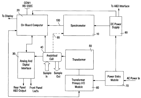
[0027] Figure 3 is a block diagram of an analyzer
using a CCD based emission spectrometer according to a
preferred embodiment of the present invention;
[0028] Figure 4 is a flowchart showing the process of
analyzing a sample spectrum for a single impurity;
[0029] Figures 5A-5C are graphs showing an example of
dark spectrum subtraction according to the process shown
in Figure 4;
[0030] Figure 6 is a graph showing an example of
baseline evaluation according to the process shown in
Figure 4;
[0031] Figure 7 is a calibration curve for use in
converting the emission peak area to an impurity '
concentration, in accordance with Step S70 of Figure 4;
[0032] Figure 8 is a graph of the dark spectrum as a
function of temperature illustrating hot pixel regions;
and
[0033] Figure 9 is a graph showing the effect of hot
pixels on baseline evaluation.
CA 02452574 2006-10-27
WO 2003/004981 PCT/US2002/020775
Detailed Description of the Preferred Embodiments
[0034] The preferred embodiments of the apparatus and
method according to the present invention will be
described with reference to the accompanying drawings.
[0035] Referring toFigure 3, a block diagram of an
exemplary analyzer using a CCD array based emission
spectrometer, which is the preferred embodiment of the
present invention, is shown. Of course, other
configurations of elements employing the CCD array based
=emission spectrometer may also be used. The analyzer
shown in Figure 3 includes a spectrometer 10, an on-board
computer 20, an analog and digital interface 30, an
analytical cell 40, a transformer 50, a transformer
primary input/output module 60, a power entry module 70,
and a DC power supply 80.
[Q036] During operation, a gas sample to be analyzed
is placed in the analytical cell 40. A preferred sample
system is the Praxair microcell described'in U.S. Patent
No. 6, 043, 881, The
advantages of the simple microcell sample system are
discussed below. The transformer 50 supplies a voltage
to the analytical cell 40 sufficient to produce a low
energy, low intensity plasma discharge from the gas
sample. A fiber-optic cable 90 transfers the light from
the emission source (i.e. the gas sample) from the
analytical cell 40 to the spectrometer 10. This CCD
array based spectrometer 10 is the heart of the system
and is described below in more detail. The spectrometer
10 determines the spectrum of the emitted light. The
spectrometer 10 has a small internal computer (not shown)
which communicates with the on-board computer 20 through
a serial link 100. The on-board computer 20 runs an
operating program that controls the analyzer. Spectra
CA 02452574 2006-10-27
= ~
WO 2003/004981 PCT/US2002/020775
11
obtained by the spectrometer 10 are sent through serial
link 100 to the on-board computer 20. The on-board
computer 20 analyzes the incoming spectra and converts
the emission lines into concentration information
corresponding to one or more impurities in the sample
gas. The on-board computer 20 receives various analog
and discrete inputs/outputs and can communicate with the
user either through these outputs, or preferably through
a direct serial connection (e.g., a RS-232C port). In
fact, most of the modules shown in Figure 3 have serial
port connections. Of course, Universal Serial Bus (USB)
connections, or any other methods for linking components,
including the use of a bus architecture may be employed.
The spectrometer's computer can also receive and carry
out a predetermined limited set of instructions. In this
manner the on-board computer 20 can control and receive
data from the spectrometer 10 without having to control
the detailed operations and internal timing of the
spectrometer 10. The transformer primary I/O module 60
allows the on-board computer 20 to control the
.transformer 50 and turn the discharge on and off as
necessary. This is critical for management of the dark
spectrum, which is discussed later.
[0037] The spectrometer 10 comprises a small handheld
optical bench and CCD detector. The light from the
emission source is brought into an entrance slit of the
optical bench. After reflecting off two mirrors and a
reflective grating, the light is dispersed onto the CCD
array. The CCD is preferably a linear array of 2,048
photodiode detector elements. Each detector element
receives light corresponding to a narrow wavelength range
(on the order of 2nm). The incident wavelength on each
photodiode is determined by the resolution of the
CA 02452574 2006-10-27
WO 2003/004981 PCT/US2002/020775
12
grating, the geometry of the optical bench, and the
position of the specific photodiode within the array. Of
course, other CCD array technologies may be employed as
desired.
[0038] CCD based spectrometers 10 are commercially
available and are lightweight, compact, and rugged. In
conjunction with the small optical bench, these CCD
arrays can cover a complete spectrum of 200nm to 800nm.
This region encompasses the far and near ultraviolet, the
complete visible, and a small portion of the near
infrared region of the electromagnetic spectrum.
[0039] To convert the incident light into an
electrical signal, each diode in the array, alt'ernatively
referred to as a pixel, is a small area of semiconductor
material connected in parallel to a small charged
capacitor. As photons strike the semiconductor material,
electron hole pairs are formed which migrate to the
opposite plates of the capacitor, causing it to slowly
discharge. After a predetermined time (i.e. an
integration time), the CCD's electronics rapidly recharge
each of the 2,048 capacitors. This recharge resets the
CCD array for the next integration period. The charge
necessary to fully recharge each capacitor is a function
of the number of photons incident on the photodiode
during the integration time. A plot of the amount of
charge incident on each photodiode during an integration
period versus wavelength reveals the spectrum of the
emission source.
[0040] An important factor is the total amount of
light incident on each photodiode during the integration
time. Because these diodes are integrating devices, the
arrival pattern of the photons is unimportant. Only the
total number of incident photons is important. In this
CA 02452574 2006-10-27
WO 2003/004981 PCT/US2002/020775
13
respect, the array acts like photographic film. A
picture can be captured in low light conditions by
leaving the shutter open for a longer period of time. In
the same way, the spectrometer's sensitivity can be
improved when using a low intensity emission source by
increasing the integration time. However, two factors
act to limit the integration time.
[0041] First, the integration time cannot be so long
that the capacitors of one or more of the diodes becomes
fully discharged during the integration time. When a
capacitor becomes fully discharged, a saturation
condition is reached and the diodes are unable to respond
to further incident photons during the remainder of the
integration period. Therefore, it is not possible to
determine differences in signal level for those pixels
that have reached saturation.
[0042] Of greater concern is the thermal noise
generated by the CCD array. If an array is left in
complete darkness, it will still generate a
characteristic noise signature. This thermal noise,
sometimes referred to as the dark spectrum, worsens at
higher temperatures and longer integration times.
Managing this temperature-dependent dark spectrum is key
to using CCD arrays with low intensity emission sources,
which require longer integration times. The present
invention addresses the problems inherent in managing
this dark spectrum so that CCDs can be practically used
with low intensity emission sources.
[0043] Now referring to Figure 4, a flowchart is shown
depicting the process whereby an analyzer constructed in
accordance with the preferred embodiment analyzes a
spectrum for impurities in a gas sample. This process
corrects the spectrum data to account for the analyzer's
_ ..~
CA 02452574 2006-10-27
WO 2003/004981 PCT/US2002/020775
14
use of a CCD array and a low-level emission source.
Figure 4 shows the steps required to generate
conceritration information for a single impurity from a
single sample spectrum. The first step S10 is to acquire
a dark spectrum from the array before the plasma
discharge is established. It is important for the dark
spectrum to be acquired using exactly the same
integration time as the subsequent sample spectra, or the
correction procedure will not work. As noted above, this
is because the characteristics of the dark spectrum are
in part a function of integration time. As discussed
previously, the dark spectrum is obtained by measuring
the CCD output when no light is incident on the array.
An exemplary dark spectrum is shown in Figure 5A. Once
the dark spectrum is acquired and stored, preferably in
the on-board computer 20, the plasma discharge is ignited
and the sample spectrum is acquired (Step S20). Figure
5B shows an exemplary sample spectrum acquired with the
same inteqration time as the dark spectrum shown in
Figure 5A. Figure 5B is a sample spectrum for an argon
gas stream containing 30 ppb of moisture impurity. In
step S30, the dark spectrum value is now subtracted on a
pixel-by-pixel basis from the sample spectrum. As shown
in Figure 5C, the resulting sample spectrum corrected for
the dark spectrum has a greatly reduced noise signature.
The remaining steps of the analysis use this corrected
spectrum (i.e. Figure 5C). Note that the 30 ppb moisture
peak at 308nm is now clearly visible in the corrected
spectrum.
[0044] The next step S40 is to determine the best
baseline underneath the emission line or peak. This step
allows the on-board computer 20 to differentiate the
light intensity of the sample gas from that of the
CA 02452574 2006-10-27 =
WO 2003/004981 PCT/US2002/020775
impurity. First, the process breaks the sample spectrum
around the emission peak into three regions. This is
shown graphically in Figure 6 for a 30 ppb moisture peak
in an argon gas sample.
[0045] The two baseline regions, baseline regions 1
and 2, on either side of the emission peak region are
used to determine the baseline. The data points in these
regions are fit to a first order regression to determine
the best fit straight line through the two sets of data.
Once the slope and intercept of this line have been
determined, a baseline value for each pixel in the
emission peak region, can be calculated. Referring again
to Figure 6, the baseline calculated based on the data in
baseline regions 1 and 2 is shown as the best fit
baseline. A straight line fit (a linear regression) is
computationally the fastest and easiest algorithm that
may be used to determine the best fit function, and
generally provides a good fit to the baseline data. If
however, the baseline region around the emission peak
contains dramatic changes, a different regression
algorithm can be used to fit. a more complex baseline.
[0046] With the baseline constructed under the
emission peak of interest, the next step S50 is to
determine the area both under the emission peak, and
under the constructed baseline in the emission peak
region. These area calculations can be performed using
any one of a number of well-known numerical integration
techniques, for example the trapezoid rule.
[0047] Once the areas of the emission peak and the
baseline in the emission peak region have been
calculated, the next step S60 is to subtract the baseline
area from the total emission peak area. The resulting
area is the area under the emission peak due to the
CA 02452574 2006-10-27
WO 2003/004981 PCT/US2002/020775
16
impurity of interest. The key point here is that the
baseline area is due to the background light level from
the plasma discharge, whereas the peak area from the
emission line is due only to the impurity of interest.
If the background level shifts for any reason it will be
reflected in the position of the baseline and the
calculated baseline area. Once the baseline area is
subtracted out, the resulting emission peak area remains
constant for a given impurity concentration.
[0048] The final step S70 is to relate the resulting
emission peak area to an impurity concentration S70.
Beforehand, a calibration curve is generated by measuring
the emission peak area for a series of known
concentration standards for the impurity of interest.
Such a calibration curve is shown for a moisture impurity
in Figure 7. From the calibration curve, an equation can
be determined that gives the concentration of moisture
for any measured emission peak area, at least over the
range covered by the calibration curve. In this manner,
the emission peak area is converted into a concentration
number (in ppb) for the impurity of interest.
[0049] This process can be repeated for any number of
emission lines in the spectrum corresponding to
impurities of interest. Examples of such impurities are
nitrogen and methane, in addition to moisture as used in
the above example.
[0050] The tremendous improvement in noise reduction
due to the subtraction of the dark spectrum is apparent
in Figure 5C. Any remaining noise due to the dark
spectrum correction would affect the baseline evaluation
algorithm and manifest itself as noise in the calculated
emission peak area and the resulting reported impurity
concentration. This would ultimately degrade the limit
CA 02452574 2006-10-27
WO 2003/004981 PCT/1JS2002/020775
17
of detection for the impurity. At the long integration
times (2-10 seconds) required to obtain the required
sensitivity, management of the dark spectrum can be
additionally addressed using the following three
complimentary approaches: 1) subtraction of the current
dark spectrum from each new sample spectrum; 2)
monitoring the temperature and the rate of change in the
temperature of the spectrometer to update the dark
spectrum when the temperature varies by more than a
certain value; and 3) dynamically masking temperature
sensitive "hot" pixels in software, so that they are
omitted from subsequent analysis. Each of these
approaches attempts to address the thermal sensitivity
problem of the CCD array. As the spectrometer warms or
cools, the initially acquired dark spectrum becomes a
poorer estimate of the correction that should be made to
the current sample spectrum. The greater the temperature
difference between the current temperature and the
temperature at which the dark spectrum was taken, the
poorer the estimate and the more noise that shows up in
the corrected sample spectrum. Temperature differences
as small as 1 C can result in unacceptable noise levels in
corrected sample spectra.
[0051] The first approach is to subtract the initial
dark spectrum for each gas sample to be analyzed.
Esseritially, this approach simply repeats step S20 to S70
in Figure 4 for each sample.
[0052] The second approach addresses thermal
sensitivity by monitoring the temperature and/or the rate
of change in the temperature of the spectrometer. To
monitor the temperature, the on-board computer 20 is
equipped with two or more redundant temperature sensors
(not shown). The computer continually monitors the
CA 02452574 2006-10-27
WO 2003/004981 PCT/US2002/020775
18
operation of the two sensors. If the primary sensor
fails, the computer uses the output from the secondary
(backup) sensor. Preferably, the sensors are located
close to the CCD array to provide an accurate indication
of the detector temperature, which is the key
measurement. The sensors may be read at regularly
predetermined intervals to provide a temperature
measurements.
[0053] The on-board computer 20 constantly evaluates
the temperature difference between the current
temperature and the temperature at which the dark
spectrum was most recently acquired and also the rate of
change of the temperature. Depending on the rate of
change, the on-board computer 20 sets an acceptable
delta-temperature. The faster the rate of change, the
larger the delta-temperature that will be allowed. This
is to avoid updating the dark spectrum, as described in
the following paragraphs, too frequently.
[0054] In normal operation, the on-board computer 20
collects and analyzes a sample spectrum typically every
30-40 seconds. If the delta-temperature is exceeded
during an analysis, the current sample is finished and
further analysis is suspended. The on-board computer 20
turns off power to the high voltage transformer 50,
thereby extinguishing the plasma discharge. The
spectrometer 10 is then instructed to acquire a new dark
spectrum while the emission source is extinguished. The
new dark spectrum replaces the previously stored dark
spectrum and the current temperature (TDARK) is recorded.
[0055] The on-board computer 20 then turns on the high
voltage transformer 50, thereby re-establishing the
plasma discharge. The on-board computer 20 returns to
normal operation and begins acquiring sample spectra
CA 02452574 2006-10-27
WO 2003/004981 PCT/US2002/020775
19
again. The computer also continues to compare the
current temperature to TDARK, where TDARK is the value at
which the latest dark spectrum was acquired.
[0056] The problem addressed by the third approach is
illustrated in Figure 8. Figure 8 is a graph of four
dark spectra - K, J, H, G - at 27 , 301, 33 , and -36 C,
respectively. As shown, the emission intensity generally
increases with temperature. Note that several groups of
pixels, notably in this example around 326nm and 344nm,
not only exhibit higher thermal noise than their
neighbors but the temperature variation is also much
greater. By identifying and then ignoring or masking
these pixels each array can be made to perform as a much
higher quality detector. This is done by categorizing
the individual detector elements into good and bad or so
called "hot" pixels. About 5% of a given CCD array can
generally be categorized as hot pixels. The number and
distribution of hot pixels is different for each CCD
array. Hot pixels typically have higher dark spectrum
values than good pixels. Research has uncovered two
other interesting and useful aspects of hot pixel
behavior. First, hot pixels tend to occur in small
contiguous groups, rather than singly. And, hot pixels
tend to get noisier in response to a temperature increase
faster than good pixels. Both of these behaviors can be
seen in Figure 8, which shows dark spectra at several
temperatures from the region of interest for moisture and
nitrogen analysis. Note the two regions of hot pixels
around 326nm and 344nm. These two groups of hot pixels
occur in the baseline region for nitrogen analysis and
may cause problems for the baseline evaluation algorithm.
[0057] For this CCD array, the effect of the hot
pixels on the baseline evaluation for nitrogen can be
CA 02452574 2006-10-27
WO 2003/004981 PCT/US2002/020775
seen in Figure 9. The data shown in Figure 9 corresponds
to an enlarged view of the region in Figure 8 containing
the two regions of hot pixels described above. Notice
the two upsets in the baseline of the spectral data 190
located around 324nm and 344nm, respectively. These
upsets correspond to the two noisy groups of hot pixels
discussed in Figure 8. These upsets cause the baseline
evaluation algorithm to generate the best fit baseline
200, shown in Figure 9. It is readily apparent that
baseline 200 is high in the emission peak region. In
fact, this baseline results in the integration algorithm
generating a negative area for the nitrogen peak emission
line, instead of the expected zero area. If the hot
pixels (i.e. the upsets) are masked, the second baseline
210 in Figure 9 is generated. Baseline 210 is
statistically a much better fit. Using this baseline
210, the peak area is calculated as zero, as is expected
for this sample.
[0058] Masks are easily generated in software by
analyzing the dark spectrum for the array. In effect, a
custom generated software mask is created and laid over
the array. The good pixels are unaffected and the bad
pixels are ignored. The operating program implements
this generated mask each time it considers using a pixel
value for either an emission line data point or a
baseline point. Thus, for a pixel to be used in an
analysis, it must be located in the right wavelength
region and be a good pixel.
[0059] Another feature of the present invention is the
use of Praxair's microcell sampling system. Praxair's
microcell sample system is described in U.S. Patent No.
6,043,881. This sample cell has=a minimal volume and no
unswept areas which helps to improve response time. With
CA 02452574 2006-10-27
WO 2003/004981 PCT/US2002/020775
21
the baseline evaluation algorithm discussed above, small
changes in sample cell pressure or flowrate have minimal
impact on the analytical results. Because of this, the
sample system can be extremely simple which again
improves response time and makes the analyzer easy to
use. The microcell has an orifice on the inlet fitting
that allows the user to connect the analyzer to the
sample point without the use of a regulator. Eliminating
the regulator, that is normally required in sample
systems, removes the single component that slows analyzer
response time the most.
[0060] The analyzer according to the present invention
is described herein as using an argon gas sample.
However, the analyzer is not limited to use with argon
and can be readily adapted for use with any noble gas,
such as helium and krypton. In addition, analyses of
hydrogen and oxygen sample gases can be accomplished.
Some exemplary impurities that can be analyzed are
nitrogen, moisture and methane. Moisture can be analyzed
in any base gas if an appropriate membrane is used.
[0061] Another approach enabling the use of longer
integration times is to thermoelectrically cool the CCD
array. Thermoelectric coolers are commercially
available, but add significant cost to the system (almost
doubling the cost) and are bulky. The temperature
compensation approaches described above can also be used
with a cooled array and will yield better detection
limits than the use of cooling alone.
[0062] The analyzer can operate over varying sample
inlet pressure ranges. Exemplary ranges span low
pressure 5-50 psig, standard pressure 20-150 psig, and
high pressure 50-350 psig. Different ranges are
available simply by changing the diameter of the critical
CA 02452574 2006-10-27
WO 2003/004981 PCT/US2002/020775
22
flow orifice in the inlet fitting described above. Each
of the ranges above corresponds to a sample flow rate of
approximately 400-2000 cc/min (0.8-4.0 cfh) through the
sample cell. Even a very low pressure version of the
analyzer can be effected by drawing a higher vacuum with
a sample pump on the analyzer vent in relation to the
inlet. The microcell can withstand operation under
vacuum conditions.
[0063] While the preferred embodiments of the present
invention have been described using specific terms, such
description is for illustrative purposes only, and it is
to be understood that changes and variations may be made
without departing from the spirit or scope of the
appended claims.