Note: Descriptions are shown in the official language in which they were submitted.
122535
CA 02452891 2003-12-11
SENSOR DEVICE FOR DETECTION OF TRANSFORMER OIL BREAKDOWN
BACKGROUND OF THE INVENTION
Field of the Invention
The present invention relates generally to the field of gas sensors. More
particularly,
the present invention relates to semiconductor gas sensors made from wide
bandgap
materials such as gallium nitride (GaN) and silicon carbide (SiC) that are
effective at
providing continuous or discrete measure of gas levels resulting from
degradation
processes in insulating oil in oil-filled high-voltage electrical equipment.
Description of the Related Art
Gas sensors have been used in the detection of particular symptomatic gases in
oil-
filled electrical equipment. Faults in oil-filled transformers, for example,
may include
arcing (electrical), corona discharge (electrical), low energy sparking
(electrical),
severe overloading (electrical), pump motor failure (electrical and thermal)
and
overheating (electrical and thermal) in an insulation system., Faults may
generate
undesirable gases, such as hydrogen (H2), acetylene (C2Hz), ethylene (CZH4),
methane
(CH4), ethane (CaH4), carbon monoxide (CO) and carbon dioxide (C02). These
fault
conditions result in a malfunctioning transformer or may indicate an impending
malfunction, which, if not corrected, may lead to failure of the transfomler.
A
statistical correlation exists between transformer malfunction and fault gases
generated by the transformer. Accordingly, if the accurate detection of
potentially
dangerous gases in a transformer is achieved, possible malfunction and failure
of the
transformer can be addressed and often avoided.
The principles described previously for oil filled transformers may also be
applied to
other pieces of oil filled equipment or facilities, in which high electrical
fields or
temperature oscillations cause the oil to break down into its potentially
flammable
constituents over time. One example of such equipment includes x-ray tubes
used in
medical applications. X-ray tubes supply x-rays used in medical assessments of
bone
1
122535
CA 02452891 2003-12-11
medical applications. X-ray tubes supply x-rays used in medical assessments of
bone
or tissue structure. These tubes, much like transformers, use oil to both
insulate and
cool internal electrical components. Gas sensors fabricated from GaN or SiC
would
provide a non-intrusive method for maintaining such equipment regularly,
minimizing
down-time and avoiding catastrophic fault conditions.
With respect to hydrogen, power transformers expose insulating oil to high
electric
fields that break down the oil over time. Hydrogen gas and hydrogen bearing
compounds are given off, indicating the need for preventative maintenance. If
this
need goes unheeded, it may lead to the build-up of flammable hydrogen gas in
the
system, which if ignited, may lead to catastrophic failure. Current detection
systems
for hydrogen include oil sampling and chromatographic analysis, single gas
sensors
and person-operated units. These conventional approaches are time consuming,
expensive, offer incomplete information, and in some cases are only performed
periodically throughout the year.
The ability of sensors to identify a target gas depends on several factors.
These
factors include the sensitivity of the sensor to other interfering gases and
vapors, and a
concentration of the target gas. The ability to resolve t:he target gas from
other gases
is called the selectivity. There are very few known sensors that are highly
selective
where a sensor has greater than about a tenfold difference in gas detection
between
sensing states and non-sensing states. Further, within these very few sensors
there are
even fewer that are relatively reliable to accurately detect individual gases.
Current semiconductor gas sensor technology may make use of Si/Si02 as
materials
on which a gas is sensed. Others may make use of SnO2 or other oxides,
however, in
the case of Sn02, these devices typically require a heater to increase their
temperature
in excess of 200 degC in order to make them sensitive enough to be useful.
While
these sensors are mass producible, they often fail in outdoor environments
where the
temperature fluctuates. Temperature fluctuations may lead to drift in response
to
gaseous environments over time, which means that the change in electrical
response
to the same gas will differ over time, thus the sensor system will require
temperature
correction in order to track quantitative changes. Even small changes in a
temperature
2
122535
CA 02452891 2003-12-11
range, such as about -40 to about 130 degF, are enough to cause such drift
over time.
Drift is most noticeable in Si devices, making these devices ineffective in
such
ambient settings. In order to minimize drift, the Si-based sensors often
require
heating to a temperature of up to about 150 degC in order to return the
sensors to
nominal operating conditions. Despite the heating, drift over time still
occurs due to
surface states formed from oxides and other elements on the surface of the
sensors.
U.S. Pat. Nos. 6,041,643, 6,155,100, 6,182,500 and 6,202,473 all issued to
Stokes et
aL, incorporated herein by reference, describe a gas sensor for determining
.the
presence of at least one gas in a gaseous environment. The gas sensor includes
a
semiconductor substrate, a. thin insulator layer disposed on the semiconductor
substrate, a catalytic metallic gate disposed on the thin insulator layer and
a
chemically modified layer disposed on the catalytic metal gate. The chemically
modified layer includes a material that protects the sensor from corrosive
gases and
interference from at least on.e of foreign matter and water, alters at least
one of surface
chemical properties and surface physical properties of the sensor, and passes
only a
designated gas therethrouglr.
What is needed is a more robust material system for addressing material issues
and
eliminating drift. What is further needed is a high temperature, harsh
environment
capable gas sensor that outperforms conventional solid-state sensors that use
semiconductor materials such as Si.
BRIEF SUMMARY OF TIDE INVENTION
In various embodiments, the present invention provides semiconductor gas
sensors
made from wide bandgap materials such as gallium nitride (GaN) and silicon
carbide
(SiC) that are effective at providing a continuous measure of gas levels in
oil-filled
high-voltage electrical equipment. These materials are more robust than
silicon (Si)
and operate well in a wide range of ambient environments. These material
systems
provide chemically stable, repeatable responses in wide temperature ranges and
harsh
environments and are effective up to about 450 degC over a wide range of
pressures.
The term harsh environment is meant to include temperatures above about 150
degC,
3
122535
CA 02452891 2003-12-11
where Si devices degrade and suffer significant reliability issues. Harsh
environments
may also include high pressures, high vibrations, a combination. therein or
other.
In one embodiment, the present invention provides a mufti-gas sensor device
comprising a semiconductor substrate, one ox more catalytic metal gate-
electrodes
deposited on the surface of the semiconductor substrate, and an ohmic contact
deposited on the surface of the semiconductor substrate. Each catalytic metal-
gate
electrode may be operable for sensing a different gas. The mufti-gas sensor
device
operates in a gaseous environment, such as immersed in electrically non-
conductive
oil containing dissolved gases.
In another embodiment, the semiconductor substrate is selected from the group
consisting of group III, IV and V materials, such as GaN, SiC.', A1N, AIGaN,
InN,
InGaN and AIInGaN. The one or more catalytic metal gate-electrodes comprise
platinum, palladium, iridium, ruthenium, nickel, copper, rhodium, molybdenum,
iron,
cobalt, titanium, vanadium, tantalum, tungsten, chromium, manganese, gold,
silver,
aluminum, palladiumailver, tin, osmium, magnesium, zinc, alloys of these
materials
and combinations of these materials.
In a further embodiment, the gases comprise hydrogen, hydrogen-bearing,
oxygen,
oxygen-bearing and others, and are a result of the degradation of oil caused
by heat
and electric fields.
In a still further embodiment, the present invention provides a gas sensor
device
comprising a semiconductor substrate, a catalytic metal gate-electrode
deposited on
the semiconductor substrate, an ohrnic contact deposited on the semiconductor
substrate, a passivation layer operable fox increasing the selectivity of the
device to a
gas and a heating mechanism. The passivation layer may comprise silicon
nitride,
silicon dioxide, silioxynitride, hafnium oxide, titanium oxide, indium doped
titanium
oxide, aluminum oxide, gallium oxide, or alloys or combinations of these
materials..
In a still further embodiment, a method is provided for detecting various
gases. The
method comprises providing a sensor device, immersing the sensor device in an
oil-
filled environment, allowing the oil-filled environment to interact with the
one or
4
122535
CA 02452891 2003-12-11
more catalytic metal gate-electrodes, altering the various gases as they
contact the
catalytic metal gate-electrodes, the altering comprising at least one of
atomically and
molecularly altering chemical structure of the various gases, and altering the
sensitivity of the sensor device. The sensor device comprises a semiconductor
substrate, one or more catalytic metal gate-electrodes deposited on the
surface of the
semiconductor substrate, wherein each of the one or more catalytic metal gate-
electrodes is operable for sensing a different gas, and an ohrnic contact
deposited on
the surface of the semiconductor substrate.
In a still further embodiment, a method for sensing various gases comprises
providing
a sensor device, immersing the sensor device in the oil-filled reservoir,
allowing the
oil to interact with the one or more catalytic metal gate-electrodes, altering
the gas as
it contacts the catalytic metal gate-electrodes, the altering comprising at
least one of
atomically and molecularly altering chemical structure of tl~e gas, and
altering the
sensitivity of the sensor device. The sensor device comprises a semiconductor
substrate, one or more catalytic metal gate-electrodes deposited on the
surface of the
semiconductor substrate, an ohmic contact deposited on the surface of the
semiconductor substrate, a passivation layer operable for increasing the
selectivity of
the device to the gas and a heating mechanism for increasing the sensor device
response to the gases.
In a still further embodiment, a method for sensing various gases comprises
providing
a sensor device, immersing the sensor device in the oil-filled reservoir,
allowing only
the gases in the oil to interact with the one or more catalytic metal gate-
electrodes by
using a protective, selectively porous membrane material, altering the gas as
it
contacts the catalytic metal gate-electrodes, the altering comprising at least
one of
atomically and molecularly altering chemical structure of the gas, and
altering the
sensitivity of the sensor device. The sensor device comprises a semiconductor
substrate, one or more catalytic metal gate-electrodes deposited on the
surface of the
semiconductor substrate, an ohmic contact deposited on the surface of the
semiconductor substrate, a. passivation layer operable for increasing the
selectivity of
the device to the gas, a heating mechanism for increasing the sensor device
response
to the gases, and a protective gate material such as a selectively porous
membrane
122535
CA 02452891 2003-12-11
which allows only certain gases to pass through it to the semiconductor device
and its
catalytic metals.
BRIEF DESCRIPTION OF THE DRAWINGS
A variety of specific embodiments of this invention will now be illustrated
with
reference to the Figures. In these Figures, Like elements have been given like
numerals.
FIG. 1 is a schematic diagram illustrating a mufti-gas sensor device
comprising three
gate-electrodes in accordance with an exemplary embodiment of the present
invention;
FIG. 2 is a schematic diagram illustrating a gas sensor device comprising one
Schottky contact in accordance with an exemplary embodiment of the present
invention;
FIG. 3 is an illustration of packaging for the mufti-gas sensor device of FIG.
1 in
accordance with an exemplary embodiment of the present invention;
FIG. 4 is an illustration of packaging for the mufti-gas sensor device of FIG.
3 further
comprising a protective gate or membrane material in accordance with an
exemplary
embodiment of the present invention;
FIG. 5 is a graph illustrating current vs. voltage characteristics of the
mufti-gas sensor
device of FIG. 1 in accordance with an exemplary embodiment of the present
invention; and
FIG. 6 is a graph illustrating the response to various concentrations of
hydrogen as a
function of time in accordance with an exemplary embodiment of the present
invention.
DETAILED DESCRIPTION OF THE INVENTION
As required, detailed embodiments of the present invention are disclosed
herein,
however, it is to be understood that the disclosed embodiments are merely
exemplary
6
122535
CA 02452891 2003-12-11
of the invention that may be embodied in various and alternative forms.
Specific
structural and functional details disclosed herein are not to be interpreted
as limiting,
but merely as a basis for the claims as a representative basis fbr teaching
one skilled
in the art to variously employ the present invention. Throughout the drawings,
like
elements are given like numerals. The systems described below apply to sensing
levels of gases in insulating oil in oil-rifled high-voltage electrical
equipment,
however, in principle also apply to any system that benefits from gas sensing.
The present invention will now be described with a sensor operating in
electrically
non-conductive oil, such as in power transformer or x-ray tube oil reservoirs,
which
are merely example applications for the sensor. The sensor may also operate in
air
and form part of an exhaust gas monitoring system for gas turbines, diesel
locomotives and aircraft engines, where the detection of gases is desirable.
The
sensor, its operation and the detection of hydrogen gas are mE;rely exemplary
and are
not meant to limit the invention.
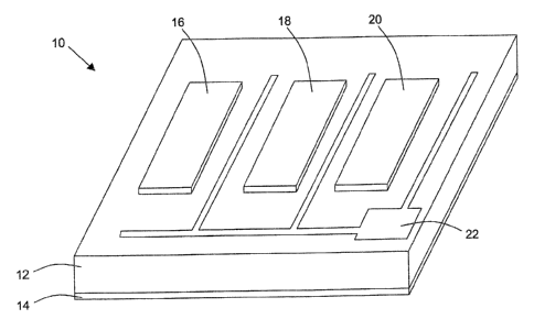
Referring now to FIG. 1, a gas sensor device 10 fox gas-in-oil detection in
high power
electrical equipment/transformers is schematically shown. The sensor device 10
may
make use of an induced electrical field at the surface of the device 10 from
hydrogen
ions, and/or hydrogen molecules that are polarized. The polarization may be
detected
by measuring current-voltage characteristics, or by measuring the capacitance
of the
device 10. This may be accomplished using several configurations such as a
diode
(Schottky) with a catalytic gate-electrode, a capacitor or a field effect
transistor (FET)
of different configurations, which use a catalytic metal as the gate.
The gas sensor device 10 comprises a mufti-electrode gas sensor fabricated on
a
semiconductor layer 12. The semiconductor layer 12 is epitaxially grown over a
substrate layer 14. The substrate Layer 14 comprises an inorganic
crystallization
growth substrate, such as sapphire, silicon, silicon carbide, aluminum oxide,
aluminum nitride, gallium nitride, gallium arsenide, aluminum gallium nitride,
lithium
gallate or any other substrate capable of supporting crystal growth on at
least a portion
of exposed area of the surface of the substrate 14.
7
122535
CA 02452891 2003-12-11
The device 10 comprises several electrode metals, each having a different
sensitivity
to different gases, making it a mufti-gas sensor. Each electrode response is
proportional to the concentration of a target gas, and the response to the
target gas is
high enough to overcome background noise. In one embodiment, the present
invention comprises a two or more terminal solid-state gas sensor device
fabricated
from a group-III/IV/V-based semiconductor epitaxial layer 12 onto which thin
metal
catalytic gate-electrodes 16, 18, 20 (e.g., Schottky contacts) are deposited.
FIG. 1
shows three gate-electrodes for exemplary purposes, however, the sensor device
10 of
the present invention may be practiced using two or more gate-electrodes
incorporated into a single large device, however, an array of different
devices is also
envisioned. Etching may be used to isolate gate-electrode components. A
potential
change of the gate-electrode 16, 18, 20 leads to a change in the electronic
equilibrium
in the underlying n- or p-type semiconductor layer 12. The sensor devise
further
comprises a thick metallic ohmic contact 22 deposited on the semiconductor
layer 12.
The gate-electrodes 16, 18, 20 serve as catalysts for a polarization layer
from a set of
gases (hydrogen, hydrogen bearing, oxygen, oxygen bearing, among others). The
metallic gate-electrodes 16, 18, 20 comprise a suitably thick layer of
material of an
appropriate corrosive-resistant gate material. For example, the materials of
the
metallic gate-electrodes 16, 18, 20 comprise an appropriate metallic material,
such as,
but not limited to at least one o~ platinum, palladium, iridium, ruthenium,
nickel,
copper, rhodium, molybdenum, iron, cobalt, titanium, vanadiurrr, tantalum,
tungsten,
chromium, manganese, gold, silver, aluminum, palladium:silver, tin, osmium,
magnesium, zinc, alloys of these materials, and combinations of these
materials.
The different catalytic metals possess different sensitivities to various
gases of
interest, making the single sensor device 10 operable for detecting several
gaseous
elements, distinguishing between them and determining concentrations. The
catalytic
gate-electrodes 16, 18, 20 have a thickness in a range preferably between
about 5 nm
to about 100 nm, more preferably from about 8 nm to about 50 nm, and even more
preferably about 20 nm in thickness. The thickness of the metallic gate-
electrodes 16,
18, 20 depend on the intended use of the sensor device 10. The level of
sensitivity for
each gas may be different for each particular gate material. The sensor device
Z O may
8
122535
CA 02452891 2003-12-11
be tuned to a particular gas by virtue of the particular gate material chosen,
and/or by
modifying the surface geometry and/or area in which each particular metal is
placed.
For high temperature applications, the gas sensor device 10 may be made up of
semiconductor materials from group-III, IV and V materials. The most conunon
alloys that may be used in the practice of the present invention comprise
binary alloys
such as GaN, InN, SiC and AIN. Ternary alloys, such as AIGaN and InGaN, and
quaternary alloys, such as AIInGaN, may also be considered for use in the
present
invention. These alloys, such as GaN and SiC, are both resistant to harsh
environments and capable of operation at high temperatures, such as over about
150
degC. In addition, the chemical inertness of GaN and SiC gives them a high
resistance to etching and degradation, even in the presence of strong acids or
bases.
The wide bandgaps of GaN and SzC make these materials ideal for the harsh
environments described above. Different semiconductor materials may be
combined
to achieve differing responses and sensitivities in arrays or single devices.
The sensor device 10 provides for the continuous, accurate and repeatable
detection of
potentially hazardous gases in an ambient environment ranging from about -40
to
about 130 degF without sensor drift, which is a common problem in currently
used Si
sensor technology. Different temperatures may be used with various diodes or
on an
array or single diode for temperature dependent variance in sensitivity to
different
gases.
A low-resistance ohmic contact 22 is necessary in the successful
implementation of
the mufti-gas sensor device 10. For example, a Ti/Al (300/710t~) or Ti/Pt/Au
(200/200/26000 layers may be deposited via conventional electron beam
evaporation
onto a GaN substrate and then may be thermally annealed at an appropriate
temperature and time (about 900 degC for about 30 sec.) using a rapid thermal
annealing technique.
Initially, hydrogen gas molecules (H2) are adsorbed onto a metallic gate-
electrode
from the surrounding ambient environment. The adsorbed molecules axe altered,
such
as by being catalytically dissociated from each other on a molecular or atomic
level.
y
122535
CA 02452891 2003-12-11
For hydrogen gas (H2), the molecules (HZ) are dissociated into individual
hydrogen
atoms (H). Next, the atomic hydrogen (H) diffuses through the metallic gate-
electrode to the interface at the semiconductor surface 12. The diffusion
forms a
dipole layer that electrically alters the Schottky barrier (height) of the
Schottky/GaN
interface. In one embodiment, the barrier height may be monitored electrically
such
as by applying a constant voltage or bias through the diode while monitoring
the
current across the diode. In another embodiment, the barrier height may be
monitored
by maintaining a constant current through the diode and observing a change in
voltage. The magnitude of change in the Schottky barrier height increases as a
gas
concentration increases, and may thereby be used to determine gas
concentration
quantitatively. Many individual gases containing hydrogen, such as, but not
limited
to, amines, mercaptans, hydrocarbons, and alcohols, may be detected in this
manner
by the sensor device 10.
GaN and SiC gas sensor devices 10 avoid the development of surface states due
to the
very slow nature of their oxidation processes, thereby increasing their
response
stability over time. This makes these semiconductor materials ideal for the
continuous monitoring of concentrations of hydrogen or hydrogen-bearing
compounds, and/or oxygen or oxygen-bearing compounds. Additionally, by using
various metals for the gate-electrodes 16, 18, 20, the sensitivity to a
combination of
gases is also possible, thereby providing for the real time monitoring of a
complex
environment, such as a transformer oil reservoir.
Deferring now to FIG. 2, an additional schematic diagram and cross-section of
the
sensor device 10 is illustrated. The sensor device 10 makes use of at least
one gate-
electrode (Schottky contact) 16 and one ohmic contact 22. A bond metal 23
serves to
make electrical contact from a wire to the catalytic metal 16, or Schottky
contact 16.
As stated above, the semiconductor layer 12 may be any n-type, p-type or
intrinsically
doped GaN, AlN, AIGaN, AlInGaN, or SiC. The semiconductor layer 12 may be
within a range of about 500 nm to several microns in thickness and is grown on
a
substrate 14. The sensor device 10 comprises at least one metal electrode (Ti
for n-
type, Pt for p-type and Al for both if so desired) for ohmic contact to the
device for
monitoring the electrical properties of the sensor device 10. The geometry of
the
to
12zs3s
CA 02452891 2003-12-11
sensor device 10 is such that the gate-electrode 16 and ohmic contact 22 are
disposed
in close proximity for increased sensitivity, preferably within about 2
microns to
about 1 mm. An oxide passivation layer 24 may be applied. to the surface of
the
sensor device 10 to passivate any dangling bonds at the surface and reduce
leakage
currents. The sensor device 10 may comprise a cover layer or may be disposed
in a
space behind a membrane, where the cover layer or membrane serve for
protection or
gas filtering to modify the concentration of reactant gases. An array of
sensor devices
may be used, each with a different cover layer or membrane that responds in a
different manner to a different gas.
Referring now to FIG. 3, an illustration of the packaging of the sensor device
10 is
shown. A packaging body 26 houses the sensor device 10, semiconductor layer 12
and heating element resistors disposed around the device 10 on the epilayer,
or
underneath the semiconductor chip 30. The heating element resistors may be
used for
generating faster response times, with the addition of heat to the surface of
the sensor.
Here, dissociated gas species that cause a response, are provided with thermal
energy
via the heating. This decreases their residency time on the surface, and thus
a faster
response from the sensor. In another embodiment, the sensor device 10 itself
may be
the heating element whereby a large current is passed through the device 10 in
order
to heat it to a temperature of about 1s0 degC. Optionally, other heating
elements such
as a metal layer disposed underneath the sensor device 10 or a thermoelectric
heater
30 disposed either underneath or on the side of the sensor device 10 may be
used.
The GaN or SiC materials used for the semiconductor layer 12 are able to
withstand
temperatures over about 4~0 degC without experiencing degradation. The
operation
of the sensor device 10 at temperatures of about 200 degC and above generally
results
in faster responses (sensitivity) to various gases.
Referring now to FIG. 4, an illustration of the sensor packaging may comprise
a
header and lid assembly 40. The header and lid assembly 40 may be soldered,
resistance welded, or epoxied to facilitate a hermetic seal. A hole may then
be drilled
through the lid and a thin film 42 may be applied across the assembly 40 to
permit the
passage of only specifically chosen atoms or molecules to the surface of the
sensor
device 10. In one embodiment, Teflon may be held in the lid mechanically using
pins
I1
122535
CA 02452891 2003-12-11
or other fastening mechanisms. ~n another embodiment, Kapton may be epoxied
around sealed edges of the lid. In yet another embodiment, a film of diamond
like
carbon may be deposited on the lid of the package to provide a corrosion-
resistant
hermetic seal. Packaging techniques in which arrays of sensor devices comprise
different membrane materials provide for selectivity among various gases.
Referring now to FIG. 5, the current-voltage (I-V) characteristics of the gas
sensor
device 10 are shown in a logarithmic plot. Here, the device behavior indicates
that in
reverse bias, the leakage current is approximately 1 microarnp at negative 10
volts,
while in forward bias, the current quickly attains levels in the milliamps or
higher.
The most important feature of this figure is the sharp increase in current
from
approximately 0 to 1 volt. As the device may be operated in or near this
voltage
range, the sharper the increase, the higher the sensitivity the sensor will
have to gases.
Referring now to FIG. b, the responses (current) of the gas sensor device 10
to various
concentrations of hydrogen as a function of time are shown. FIG. 5 highlights
the
strong response of the sensor device 10 to hydrogen as operated. This data
also shows
that once the gas concentrations are lowered (e.g. from 1 °lo HZ to 0.1
% HZ), the
current in the device follows that trend. Although this figure illustrates the
response
of a gas sensing diode operated in the constant voltage mode, it may also be
operated
in the constant current mode. In this case, a designated current level is
applied to the
diode, and the resulting voltage is measured. This method also has the
advantage that
as the current is held constant throughout the measurement, so is the internal
(resistive) heating level. Thus, the epitaxial layers (and surface) see the
same heating
during the range of gases exposed, which is converse to the constant-voltage
mefhod
of measurement.
In the FET type device of the present invention, the FET structure is a
natural
amplifier, i.e. a small change in the Schottky potential may cause large
changes in the
channel current, which makes the sensor device 10 more sensitive. By using a
silicon
nitride (Si3N4) passivation layer, the sensor device may mitigate effects of
surface
states that may potentially cause false signals due to an interaction of the
surface
states with positive ions other than hydrogen. The Si3N4 layer thereby
increases the
12
122535
CA 02452891 2003-12-11
selectivity to hydrogen as the hydrogen interacts with the semiconductor layer
by
diffusing through the metallic gate, whereas the other large molecules are
prevented
from interacting with the surface. Further improvements to sensitivity may be
accomplished by adding a Teflon or Kapton cover to the sensor device 10. Some
variations of Teflon material has a selectivity of about 10:1 for HZ:OZ or
greater,
which provides increased sensitivity. Kapton's selective porosity is even
greater, near
20:1. The Teflon or kapton cover may be used to filter gas compounds from a
main
cell in an extraction cell for increased gas concentrations.
There are several methods for which measurement data may be extracted from the
described sensor embodiments. These include measuring a sensor's electrical
current
while applying a constant voltage, or measuring a voltage while applying a
constant
current. Additionally, the capacitance of a device may also be measured, as
the
capacitance is modified with gas concentration. All of these methods or
combinations
of them may be applied to a single, two electrode device such as a diode,
capacitor, or
a three electrode transistor. These or other methods also exist for extracting
a
simultaneous measurement of two or more gases, using the same types, or
extensions
of these device configurations.
To facilitate the measurement of two or more gases, an array of individual
devices or
a larger device incorporating multiple features may be used. These multiple
features
may include a large fingered device as shown in FIG. 1, whereby finger 16 is
comprised of one catalytic metal, finger 18 is comprised of a second and
finger 20 is
comprised of a third and so on. As different catalytic metals have differing
catalysis
mechanisms to many gases, these may be taken advantage of in the simultaneous
sensing of more than one gas species (e.g. ethylene, methane and hydrogen) to
form a
multi gas sensor.
In another embodiment of a mufti gas sensor, one may modify the temperature of
individual devices separately, or individual sections of a larger device. For
example,
individual heating (or cooling) elements rnay be used to separately and
differently
heat finger 16, from finger 18 from finger 20. A modification in the
temperature of
the surface of a finger will cause a modification in the desorption rate of
reacted gas
13
122535
CA 02452891 2003-12-11
species from the surface. By measuring the rata at which each separately
heated (or
cooled) section or finger turns on or off rnay describe the gas species
present.
Additionally, fingers I6, 18 and 20 may be comprised of different catalytic
metals
that have varying responses to different gases. An algorithm may be then
applied to
extract information about separate gases.
It is apparent that there have been provided, in accordance with the device
and
methods of the present invention, a sensor device for gas-in-oil detection.
Although
the device of the present invention has been described with reference to
preferred
embodiments and examples thereof, other embodiments and examples may perform
similar functions and/or achieve similar results. All such equivalent
embodiments and
examples are within the spirit and scope of the present invention and are
intended to
be covered by the following claims.
m