Note: Descriptions are shown in the official language in which they were submitted.
CA 02453065 2003-12-11
Titles Incomplete Mechanical Contacts For Il~icrowave Switches
FIELD OF THE INVENTION
[0001, The invention relates to structural features for the contact
members of a switch contact. In particular, the invention provides structural
features for the contact members of a microwave switch contact that facilitate
an incomplete mechanical contact with a reduced stress distribution when the
contact members are in contact with one another.
BACKGROUND OF THE INVENTION
[0002, Microwave switches are often used in satellite communication
systems where performance, reliability and lifetime of system components are
important. These parameters relate to the contact resistance of a microwave
switch. In particular, microwave switches require low DC contact resistance,
low insertion loss (i.e. the attenuation between the input and output ports of
an activated path) and low impedance mismatch for good RF performance.
Heat dissipation and insertion loss due to conductor and reflection losses
increase for microwave switches with increased contact resistance.
Furthermore, the life of a microwave switch is expressed as the number of
actuation cycles for which the contact resistance does not deteriorate above a
certain limit.
[0003] A microwave switch contact involves the physical engagement
or contact of a first contact member by a second contact member. As it is
known to those skilled in the art, the first contact member is a fixed contact
also known as a probe and the second contact member is a moveable contact
also known as a reed. The contact resistance and the life of the microwave
switch are determined by the regions of the reed and probe that come into
contact with each other (hereafter referred to as contact regions). The
contact
interface is herein defined as the surface of the contact members that are in
physical contact with one another. To reduce ohmic losses, each contact
member is typically plated with a conductive material having a high electrical
conductivity like a metal such as gold.
CA 02453065 2003-12-11
-2-
[0004] Most prior art microwave switches have probes and reeds with
contact regions that are flat surfaces. However, it is not preferable to use
flat
surfaces for both contact regions since there is a high degree of stress at
the
edges of flat contact regions. This stress may result in the excessive plastic
deformation of at least one of the contact regions in which the yield strength
of
the material is exceeded. This in turn increases the contact resistance and
decreases the lifetime of the switch contact members.
[0005] In order to address these issues, contact theory and the
electrical junction between the probe and reed contact regions must be
examined. The electrical junction comprises a plurality of spots, known in the
industry as a-spots, that provide a multitude of parallel, microscopic
electrical
and mechanical connections between the probe and the reed contact region.
The number and shape of the a-spots depend on the surface roughness of
the contact regions and the contact pressure. The a-spots are located in
clusters having a position and a diameter that is determined by the radii of
the
contact regions, the material properties (i.e. modulus of elasticity and
Poisson
ratio), large-scale waviness of the surface of each contact region and the
contact pressure distribution. The contact pressure distribution is the
distribution of the contact force on the contact interface. Although
mechanical
contact occurs at many a-spots, electrically conductive a-spots do not occur
at
surface insulating layers such as oxide films. Accordingly, the total contact
resistance is a summation of bulk resistance, constriction resistance (i.e.
the
resistance of the a-spots) and film resistance (due to surface films and other
non-conducting contaminants in the contact interface) (P. G. Blade (1999),
Electrical Contacts: Principle and Applications, pp 4-15).
[0006] Research has shown that for contact surfaces having an
anisotropic micro-topography, the a-spot distribution has an elliptical shape
with a spreading resistance that is given by:
f b (1)
c
CA 02453065 2003-12-11
-3-
where a and b represent the semi-axes of an elliptical a-spot, a~ is the
radius
of a circular a-spot having an area identical to that of the elliptical a-spot
and
the function f is a form factor related to experimental data. The form factor
decreases from one to zero as the aspect ratio (alb) increases from one
towards infinity (P. G. Slade, Electrical Contacts: Principles and
Applications,
New York, Marvel Dekker, Inc., pp. 4-15, @1999). The spreading resistance
is half of the contact resistance in the absence of insulating films between
the
reed and probe contact regions.
(000?] Contact theory describes three different types of contact
interaction from a mechanical point of view: incomplete mechanical contacts,
complete mechanical contacts and receding mechanical contacts (K.L.
Johnson, Contact Mechanics, Cambridge lJniversity Press, @1985).
Incomplete mechanical contacts comprise non-conformal contact members
(i.e. contact members which do not have identical contact regions). When the
contact members are pressed together, the area of the contact interface
increases in size as the applied contact force increases. The initial contact
is
made at a point or a line, which then increases into a curvilinear region as
the
applied contact force increases. The contact pressure approaches zero at the
edges of the contact interface. Consequently, the a-spot clusters are located
towards the center of the contact interface and the contact resistance is
independent of the distribution of the a-spots (J. A. Greenwood, "Constriction
Resistance and the Real Area of Contact", Brit. J. Appi. Phys., 3,277,1970; M.
Nakamura et al., "Computer Simulation for the conductance of a contact
interface", IEEE Trans. Comp. Hybrids Manuf. Technol., CHMT-9, p. 150,
1986; I. Minowa et al., "Conductance of Contact Interface depending on
Location and ~istribution of Conducting Spots°°, Proc.
Electrical Conference
on Contacts, Electromechanical Components and Their Applications, p. 19,
1986). This is beneficial for having a consistent contact resistance that is
fairly
stable during a plurality of contact actuations. This is also beneficial for
manufacturing batches of probes and reeds which all have a relatively similar
contact resistance that is predictable. furthermore, for contact members with
non-conformal contact surfaces, Hertz theory predicts that the maximum of
CA 02453065 2003-12-11
the contact stress occurs at a certain depth from the surface of the contact
interface.
[0008] Complete mechanical contacts comprise contact members
having conformal surface geometries (K. L. Johnson, Contact Mechanics,
Cambridge University Press, @ 1980. Consequently, the contact pressure
has a singularity (i.e. the stress magnitude is extremely high) at the edges
of
the contact interface. This may lead to excessive plastic deformation in the
regions of the contact members situated in the vicinity of the edges, which
reduces the lifetime of the switch. Furthermore, in a complete contact, the a-
spots are distributed close to the periphery of the contact interface.
Consequently, contact resistance is no longer independent of the distribution
of the a-spots. Accordingly, the contact resistance may vary across
consecutive contact actuations and is sensitive to manufacturing variability.
This results in a degradation of the RF performance of the microwave switch.
[0009] Receding mechanical contacts comprise contact members
having surface geometries that, when pressed together, result in a contact
interface having an area that decreases when the applied contact force
increases (Hill, Mechanics of Elastic Contacts, Putterworths-Heinemann Ltd.,
a~1993). A receding contact is specific to thin membrane contacts having a
low stiffness. Receding mechanical contacts are usually not applicable to
microwave switches due to their low stiffness.
[0010] Prior art attempts to address the issue of contact resistance
involve using probes and reeds that have conformal contact regions (such as
two flat surfaces). Unfortunately, contact members with conformal contact
regions behave as complete mechanical contacts. This is disadvantageous for
the reasons specified above. Furthermore, this structure for the reed and
probe contact regions does not allow for controlled wiping. elViping involves
cleaning the surface of the probe and reed contact regions from minor films
and brushing aside particulate contamination. This is beneficial since minor
films and non-conducting particles on the contact interface increase contact
resistance. Accordingly, wiping will reduce contact resistance and improve
CA 02453065 2003-12-11
-5-
contact performance (K. E. Pitney, NEY Contact Manual: Electrical Contacts
for Low-Energy Uses, The J. M. NEY Company, 197.3).
[0011] Another prior art method to improve contact resistance involves
using texture features for the contact region. It is well known to those
skilled in
the art that a very low and consistent contact resistance may be obtained by
imposing a surface texture having a roughness on the surface of the harder
plated layer of the probe, for example. The roughness has a certain lay, which
provides for elliptical a-spots when the contact regions of the probe and the
reed are in contact with one another. In this case, there is a reduction in
contact resistance because the a-spots have an elliptical shape with a high
aspect ratio (i.e. the semi-axis length b is much larger than the semi-axis
length and contact resistance decreases due to the effect in Equation 1 ).
Furthermore, the contact interface area is larger since the softer plated
layer
on the reed (usually) contact region deforms around the asperities (i.e.
microscopic surface peaks) of the harder plated layer on the probe contact
region. In addition, an optimal surface texture may locate the a-spot clusters
near the center of the apparent contact area. I-Iowever, it is difficult to
repeatably manufacture the surface texture on the probe since the surface
texture and the lay direction are difficult to specify and measure.
Accordingly,
the contact resistance varies across different/ manufactured batches of
switches. Furthermore, 'the contact regions of the probe and the reed form a
complete mechanical contact, which results in a reduction in the life of the
switch for the reasons specified above.
SUMMARY OF THE 9N1~ENTION
[0012] The present invention is directed to surface features of the
contact regions of reeds and probes to provide a switch contact having an
improved contact resistance, thereby providing increased reliability and
longer
lifetime. The surface features described herein are applicable to a wide range
of microwave switches such as, but not limited to, S-switches, C-switches,
T-switches, SPnT switches and R-switches. The surface features result in
contact members, which have non-conformal contacts thereby providing an
CA 02453065 2003-12-11
-6-
incomplete mechanical contact. These non-conforming contacts may include
the combination of a flat surface contact with a convex surface contact or of
two contact convex surfaces. Regardless of the combination of non-
conforming contact regions, the contact region which has a curved surface
with a radius of curvature that is determined by the material properties of
the
contact members, the magnitude of the contact forces and the dimensional
limitations of the contact regions imposed by the RF requirements. This radius
of curvature is determined such that there is a reduction in the contact
stress
distribution within the contact members. Preferably, the maximum contact
stress occurs within the metallic substrate region of at least one of the
probe
and reed contact members so that excessive plastic deformation of the
contact members does not occur. This includes reducing the stress in the
plated layer of the contact members.
[0013] In addition, the various embodiments of the non-conforming
contact members are robust to misalignments and provide a good controlled
wiping action. Furthermore, the non-conformal surfaces used for the contacts
do not result in large manufacturing variations since the required surfaces
are
surfaces of revolution that are easily generated.
[0014] In a first aspect, the present invention provides a switch contact
for use in a microwave switch. The switch contact comprises a probe contact
member having a first surface, and a reed contact rr'ember having a second
surface. The second surface is non-conformal with respect to the first surface
for providing an incomplete mechanical contact. ~uring contact, a contact
stress distribution exists having a maximum stress value at a location within
the contact members. A~t least one of the surfaces has a radius of curvature
selected to adjust the location of the maximum stress value for reducing the
magnitude of the contact stress distribution within the contact members.
(0015] Preferably, the microwave switch comprises an RF module, an
actuation module in communication with the RF module, and a control module
in communication with the actuation module. The RF module has a plurality of
the probe contact members and a plurality of the reed contact members. Each
CA 02453065 2003-12-11
-7-
of the reed contact members has a transmitting state to electrically connect a
pair of the probe contact members, and a non-transmitting state to
electrically
isolate the pair of probe contact members, thereby defining a switch
configuration for the microwave switch. The actuation module has an actuator
for moving at least one of the reed contact members into a transmitting state
and moving the remainder of the reed contact members into a non-
transmitting state. The control module receives command signals to control
the switch configuration by providing signals to the actuation module.
(0016 In another aspect, the present invention provides a switch
contact for use in a microwave switch. The switch contact comprises a probe
contact member having a first surface, and a reed contact member having a
plurality of fingers each having a second surface. The first and second
surfaces are non-conformal. During contact, the first and second surfaces
provide an incomplete mechanical contact and the plurality of fingers provide
a plurality of contact regions for reducing contact resistance.
[0017 in another aspect, the present invention provides a switch
contact for use in a microwave switch. The switch contact comprises a probe
contact member having a first surface and a reed contact member having a
second surface with a radius of curvature. The second surface is non-
conformal with respect to the first surface for providing an incomplete
mechanical contact when the contact members are in contact.
[0018] In another aspect, the present invention provides a switch
contact for use in a microwave switch. The switch contact comprises a probe
contact member having a first surface with a toroidal shape, and a reed
contact member having a second surface. During contact, the first and second
surfaces define a non-conformal contact having a contact interface located
along a circular arc on a curved portion of the toroidal shape.
[0019, In another aspect, the invention provides a method of reducing
stress distribution in a switch contact for a microwave switch, the switch
contact comprising a probe contact member having a first surface, and a reed
contact member having a second surface. The method comprises:
CA 02453065 2003-12-11
-
a) selecting the first and second surfaces to be non-conformal
for providing an incomplete mechanical contact, at least one of the surfaces
having a radius of curvature;
b) calculating contact stress distributions within the contact
members for several values of the radius of curvature; and,
c) selecting a desired radius of curvature from the several
values of the radius of curvature for reducing the contact stress distribution
within the contact members.
BRIEF DESCRIPTI~N ~F THE DRAIItfINGS
[0020] For a better understanding of the invention and to show more
clearly how it may be carried into effect, reference will now be made, by way
of example only, to the accompanying drawings which show preferred
embodiments of the invention and in which:
[002'9] Figure 1a is a block diagram of the components of a typical prior
art microwave switch;
[0022] Figure 1b is a diagram of an RF cover for a prior art RF module;
[0023] Figure 1c is a diagram of a corresponding prior art RF head for
the RF cover of Figure 1b;
[0024] Figure 1d is a partial sectional view of the prior art RF cover of
Figure 1b attached to the prior art RF head of Figure 1c;
[0025] Figure 1e shows the probe and reed contact configurations
during the operation of a prior art T-switch;
(0026] Figure 2a is a partial view of an RF module having probes and
reeds with non-conformal contact regions in accordance with the present
invention;
[0027] Figure 2b is a magnified view of the reeds and probes of Figure
2a showing a contact made between a long reed and a probe;
[0028] Figure 2c is a magnified view of the reeds and probes of Figure
2a showing a contact made between a short reed and a probe;
CA 02453065 2003-12-11
_g_
[0029] Figure 2d shows a curvilinear contact interface formed during
the initial contact of a reed and probe shown in Figures 2a to 2c;
[0030] Figure 2e shows a curvilinear rectangular contact interface
formed when there is an increased contact force between a reed and probe
shown in Figures 2a to 2c;
[0031, Figure 2f is a plot of Von Mises stress versus depth for several
probe-reed contact configurations;
[0032] Figure 2g is a plot of Von Mises stress versus depth for a
contact member having two different radii of curvature;
[0033, Figure 3a is a partial view of an RF module having an alternative
embodiment of probes and reeds with non-conformal contact regions in
accordance with the present invention;
[0034) Figure 3b is a magnified view of the reeds and probes of Figure
3a showing a contact made between a short reed and a probe;
[0035] Figure 3c shows a curvilinear contact interface formed during
the initial contact of a reed and probe shown in Figures 3a to 3b;
[0036] Figure 3d shows the contact interface formed when there is an
increased contact force during contact between a reed and a probe of Figures
3a and 3b;
[0037, Figure 4a is a partial view of an RF module having another
alternative embodiment of probes and reeds vmith non-conformal contact
regions in accordance with the present invention;
[0038] Figure 4b is a magnified view of the reeds and probes of Figure
4a showing a contact made between a long reed and a probe;
[0039, Figure 4c is a magnified view of the reeds and probes of Figure
4a showing a contact made between a short reed and a probe;
[0040] Figure 5a is a partial view of an RF module having another
alternative embodiment of probes and reeds with non-conformal contact
regions in accordance with the present invention;
CA 02453065 2003-12-11
-10-
[0041, Figure 5b is a magnified view of the reeds and probes of Figure
5a showing a contact made between a long reed and a probe;
[0042, Figure 5c is a magnified view of the reeds and probes of Figure
5a showing a contact made between a short reed and a probe;
[0043, Figure 5d is a diagram of a probe having a conical contact
region;
[0044, Figure 5e is a diagram of a probe having a spherical contact
region;
[0045) Figure 6a is a partial view of an RF module having another
alternative embodiment of probes and reeds with non-conformal contact
regions in accordance with the present invention in which the probes have a
flat contact region and the reeds have a brush-type contact region;
[0046) Figure 6b is a partial view of an RF module having another
alternative embodiment of probes and reeds with non-conformal contact
regions in accordance with the present invention in which the probes have a
toroidal contact region and the reeds have a brush-type contact region; and,
[00471 Figure 6c is a diagram of an alternative embodiment for the
reeds of Figures 6a and 5b;
DETAILED DESCRIPTION OF ThIE INVENTION
[0048) There are a variety of microwave switch structures such as
SPDT-switches, C-switches, SPnT swatches, S-switches, T-switches and R-
switches. An SPDT-switch has three probes (one input probe and two output
probes) and two conductor paths. A C-switch has four probes (two input
probes and two output probes) and four conductor paths. A T-switch has four
probes (two input probes and two output probes) and six conductor paths. An
R-switch is very similar to a T-switch and has four probes (two input and two
output probes) and five conductor paths. A number of switch-configurations
are known for these microwave switches, most of which have their own
specific type of actuating mechanisms. However, each microwave switch has
CA 02453065 2003-12-11
-11-
certain basic components. The present invention is applicable to each of
these types of microwave switches.
[0049 Referring now to Figure 1a, shown therein is a block diagram
illustrating the typical components of a microwave switch 10. This is but one
embodiment of the microwave switch 10 shown for exemplary purposes and
is not meant to limit the invention. The microwave switch 10 may be a single-
pole double-throw switch or a partial view of a double-pole double-throw C-
switch or a T-switch. The microwave switch 10 generally comprises an RF
module 12, an actuator module 14 and a control module 16. The RF module
12 has a housing 18 that comprises an RF head 0 and an RF cover 22 (see
Figures 1b, 1c and 1d for an exemplary embodiment). The RF head 12
comprises RF connectors 24 each having a probe 28. The connectors 24
provide a connection between the microwave switch 10 and the coaxial
transmission lines (not shown). The RF head 20 further comprises reeds 28
and 30 each having a dielectric pin 32 and 34 that houses a permanent
magnet 36 and 38. The permanent magnets 36 and 38 in general do not have
to be of the same polarity. Underneath the RF cover 22 rotates a disk 40
having permanent magnets 42 and 44. The permanent magnets 42 and 44 in
general do not have to be of the same polarity. However, the combination of
the permanent magnets 36, 38, 42 and 44 have to be such that when, for
example, the pair of magnets 36 and 42 and 38 and 42 will attract, while the
pair of magnets 36 and 44 and 38 and 44 will repel or reverse. Accordingly, by
rotating the disk 40, one of the reeds 28 or 30 will cantact two of the probes
24 and the other reed 28 or 30 will not contact the probes 24.
[0050 The actuator module 14 comprises a drive mechanism or
actuator 46 that controls the rotation of the disk 40 so that one of the reeds
28
and 30 contacts two of the probes 24. In the example shown in Figure 1a, the
actuator 46 may be a stepper motor such as a rotary permanent magnet
stepper motor or a rotary variable reluctance stepper motor. The stepper
motor is connected to the disk 40 via a drive shaft 48 along with an
CA 02453065 2003-12-11
-12-
appropriate bushing or ball bearing 50. Alternatively, a mechanical camshaft
may be used.
[0051, The control module 16 has an electrical interface with a printed
circuit board comprising feed through pins that provide DC command signals
to the actuator module 14. In particular, the DC command signals are sent to
the windings of the stepper motor in the actuator module 14 to excite one of
the windings to place the microwave switch 10 in a desired switch
configuration. The DC command signals comprise pulses having a certain
duration and polarity. Both positive and negative DC command signals may
be used. The control module 16 further comprises a telemetry interface that
comprises appropriate electronics to provide an indication of the
configuration
of the microwave switch 10. In this example, the control module 16 comprises
a telemetry arm 52 having telemetry magnets 54 and 56. The telemetry arm
52 is connected to the actuator 46 via a second drive shaft 58 with a second
appropriate bushing or ball bearing 60. The telemetry arm 52 rotates together
with the disk 40. The orientation of the magnets 54 and 5 6 provide an
indication of the configuration of the microwave switch 10 by interacting with
various telemetry reeds one of which is indicated at 62. Thus for each of the
microwave switch 10 positions, a unique reed switch configuration exists in
the control module 16. More details about the operation of the microwave
switch 10 are provided in U.S. 5,065,125 and U.S. 5,4.99,006.
[0052, Referring now to Figure 1b, shown therein is a top view of an RF
cover 70 in accordance with an exemplary embodiment of a prior art T switch
having three long reeds 72, 74 and 76 as well as three short reeds 78, 80 and
82. The RF cover 70 is preferably made from aluminum. Using reed 72 as an
example, each reed has a first end 72a and a second end 72b which each
have a contact region on an upper surface thereof. Each reed is connected to
a pin 72c having an internal bore 72d that houses a permanent magnet (not
shown). The pin 72c is inserted through a hole (not shown) in the reed 72 and
is secured to the reed 72 via a fastener 72e. The reeds 72, 749 76, 78, 80 and
82 are separated into three sets to define three unique RF switching
CA 02453065 2003-12-11
-13-
configurations (see Figure 1 e). The RF cover 70 has several apertures 84 for
allowing connection to a corresponding actuator module.
[0053] The RF cover 70 further comprises central walls 86, 88 and 90
and outer walls 92, 94 and 96, which are oriented to provide a plurality of
waveguide channels within the RF cover 70. There are six waveguide
channels with the RF cover 70 which have three ground planes comprising
two side ground planes provided by two of the walls 86, 88, 90, 92, 94 and 96
and an upper ground plane provided by the underside of the RF cover 70
within each of the waveguide channels. A coaxial transmission line path is
created between a pair of probes (not shown) when the pr~bes are connected
by an appropriate reed 72, 74, 76, 78, 80 or 82. The RF cover 70 further
comprises a plurality of guide pins 98 (two of which are labeled for
simplicity).
The guide pins 98 are made of a dielectric material and are used to insure
that the reeds 72, 74, 76, 78, 80 and 82 move in a linear fashion when
actuated. The guide pins 98 further insure that the reeds 72, 74, 76, 78, 80
and 82 do not contact the walls 86, 88, 90, 92, 94 and 96 during actuation.
The guide-pins 98 may be of Ultem~, or some other dielectric material. The
RF cover 70 is made from Aluminum and is preferably plated to reduce wear
from possible impacts from the reeds 72, 74, 76, 78, 80 and 82.
(0054] Referring now to Figure 1 c, shown therein is a bottom view of a
RF head 100 which is preferably made from aluminum and is configured to
engage the RF cover 70. Accordingly, the RF head 100 comprises a plurality
of fasteners 102 which protrude through the apertures 84 in the RF cover 70
to attach the RF head 100 and the RF cover 70 to a corresponding actuator
module 14.
[0055] The RF head 100 further comprises four probe connector
assemblies 104, 106, 108 and 110 which are mounted within the RF head
100. Using probe connector assembly 104 as an example, each probe
connector assembly 104 has a connector shell 104a for mechanically
engaging a coaxial cable (not shown) and a probe contact region 104b that is
connected to the inner conductor of the coaxial cable. The outer conductor of
CA 02453065 2003-12-11
~- 14 -
the coaxial cable is connected to RF head 100 through the connector shelf
104a of the probe connector assembly 104. Several types of connectors may
be used for the connector assembly 104 such as but not limited to, an SMA
connector, a TNC connector and an N connector. The particular type of
connector used depends on the amount of power that is delivered to the
microwave switch. The probe contact region 104b is physically engaged by a
reed contact region when a reed is moved towards the probe 104 to make
contact therewith. The probe 104 is mounted within the RF head 100 such
that the connector shell 104a is located on the outside of the RF head 100
and the probe contact region 104b is located in the interior of the RF head
100.
[0056] Referring now to Figure 1d, shown therein is a partial cross-
sectional view of an RF module 120 that comprises the RF cover 70 and the
RF head 100. Connectors 122, 124, 126, and 128 (not shown) protrude from
the bottom of the RF head 100. Two probes 130 and 132 are shown which
correspond to the connectors 124 and 126 respectively. The probes 130 and
132 each have a probe contact region 134 and 136 respectively. Also shown
are reeds 138, 140 and 142 and two pins 144 and 146 each having a magnet
148 and 150. Also shown is an RF cavity 152 that extends throughout the
interior of the RF cover 70 and the RF head 100 and is comprised of the
waveguide channels formed between the central walls and the outer walls
shown in Figure 1 b. Since the coupling between the reedlpin assemblies and
the actuator (see Figure 1a) is magnetic, the RF module 120 was designed as
a self contained, "sealed" unit to reduces the leakage of electromagnetic
fields.
[0057] During T-switch operation, two of the reeds in the RF cover 70
are moved towards the probes to creafie two continuous coaxial transmission
fine paths (the various configurations of the contacting reeds and probes
during the operation of a T-switch are shown in Figure 1e). The transmission
line path geometry of the RF channel is designed to provide an RF coaxial
line with characteristic impedance Zo (typically 50 ohms). This provides an
CA 02453065 2003-12-11
-15-
impedance match with the impedance of the coaxial transmission lines that
are connected to the connectors. The other four reeds are kept adjacent to
the upper ground plane in the interior of the RF cover 70. In Figure 1d, reeds
138 and 142 are shown in a non-transmission state. The geometry of a
waveguide is designed so that the cutoff frequency is higher than the
operating frequency of the microwave switch. Accordingly, there is a high
level of isolation between the probes that are associated with a non-
transmitting waveguide path.
[0058) It is well known to those skilled in the art that the probes and
reeds of microwave switches are plated with pure gold or gold alloys.
Referring to Figure 1d, the contact regions of the probes and reeds of prior
art
microwave switches have flat surfaces as shown at contact regions 154, 156,
158 and 160. Accordingly when the contact region 156 of the reed 140
physically contacts the contact region 154 of the probe 132, a complete
mechanical contact is formed. This results in increased values of stress
occurring at the edges of the contact interface, which may lead to excessive
plastic deformation of the contact regions. Consequently, the lifetime of the
microwave switch is reduced and contact resistance varies between
successive actuation.
[0059] It is desirable for the RF module 120 to have good RF
performance. Accordingly, the contact regions in the RF module 120 are
preferably designed to have low ohmic losses, good heat transfer properties
and the ability to handle mechanical loads. To achieve these goals, it is well
known in the art to construct the contact regions from a structural material
or
substrate that is capable of withstanding the required mechanical loads and
can provide good heat transfer properties such as copper or a copper alloy
such as beryllium copper. The substrate is then plated with a thin layer of
very
low resistivity material, which does not erode or corrode easily such as pure
gold or a gold alloy. This is possible because at microwave frequencies,
current flow in metals is essentially a surface phenomenon in which the entire
current flow takes place in a thin surface layer having a thickness of
CA 02453065 2003-12-11
-16-
approximately three skin depths (the skin depth is related to the frequency of
the current and the relative permeability and electrical conductivity of the
material used for the plating layer). Gold also has a high resistance to
surface
film formation. However, gold and gold alloys are characterized by reduced
mechanical properties like tensile strength, yield strength, hardness etc in
comparison to the substrate material.
[0060] During the operation of the microwave switch 10, a contact
stress distribution exists in the plating layers and the metallic substrates
of the
contact members. The magnitude of the stress distribution is such that the
plating layers undergo a degree of plastic deformation. Unfortunately, in the
prior art, care was not taken to reduce the magnitude of the stress
distribution
and in many cases the resulting degree of plastic deformation was excessive
to the point of producing excessive wear and tear on the contact members.
This in turn results in increased contact resistance and decreased reliability
and lifetime of the switch contact.
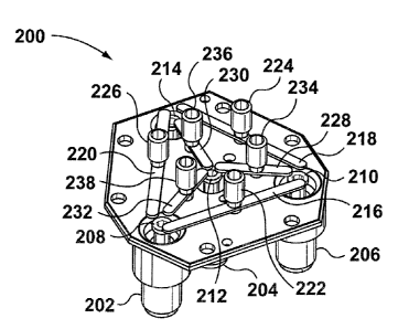
[0061] Referring to Figure 2a, shown therein is a partial view of an RF
module 200 for a T-switch in which the RF cover, dielectric pins and internal
walls have been removed. The RF module 200 has connectors (of which only
three are shown) 202, 204 and 206 and four probes 208, 210, 212 and 214
each having toroidal contact regions. Also shown in Figure 2a are three long
reeds 216, 218 and 220 each having pins 222, 224 and 226 respectively as
well as three short reeds 228, 230 and 232 each having pins 234, 236 and
238 respectively. Each reed has flat contact regions.
[0062] The reed and probe contact regions shown in Figure 2a have
non-conformal surfaces thus providing for an incomplete mechanical contact
when a reed contacts a probe. The contact may be described as a cylindrical
contact region making contact with a flat contact region. In particular, the
toroidal surface of the probe contact region 208a (see Figures 2b and 2c) has
a radius of curvature that is determined by the material properties of the
contact regions, the magnitude of the contact forces, and the dimensional
limitations imposed by the RF requirements of the microwave switch. Since
CA 02453065 2003-12-11
-17-
contact regions of the reeds and the probes of Figure 2a form incomplete
mechanical contacts, a number of advantages are provided such as the
formation of contacts having a contact resistance that is independent of the a-
spot distribution. This results in a fairly stable contact resistance across
many
contact actuations. Furthermore, the contact pressure distribution approaches
zero at the edges of the contact interface with the maximum amount of stress
occurring at a certain depth underneath the surface of the probe contact
interface. The radius of curvature is also selected to vary the location of
the
maximum contact stress which reduces the magnitude of the contact stress
distribution within the contact members as discussed further below.
'0063 Referring now to Figure 2b, shown therein is a contact in which
the first contact member is the reed 216 and the second contact member is
the probe 208. In particular, the contact region of the reed 216 comprising a
flat surface 240 has contacted the contact region of the probe 208 comprising
a portion of the toroidal surface 208a to form a line contact interface 242.
The
other two reeds 220 and 232 do not make contact with the probe 208 since
only one reed may contact a probe at a time in this example. The contact
interface begins as a curved line 242 (see Figure 2d) along which the a-spot
clusters are located which then turns into a curvilinear region 244 (see
Figure
2e), which appears as a portion of an annulus. As can be seen, the probe 208
and the reeds 216, 220 and 232 are configured so that there is enough room
for more than one reed 216, 220 and 232 to contact the probe 208 although
only one reed 216, 220 and 232 may contact the probe 208 at a time in this
example.
(0064) In addition, the contact interface occurs along an arc on a
curved portion of the toroidal surface 208a of the probe 208 so that the reed
232 contacts the outer curved surface of the toroidal surface 208x. This has
advantages such as providing a greater degree of wiping as explained further
below. Those skilled in the art will also realize that the contact made is a
"frontal" contact rather than a "side" contact which is beneficial since a
'°side"
CA 02453065 2003-12-11
-18-
contact results in increased stray capacitance. These observations also hold
for other embodiments discussed below.
(0065] Referring now to Figure 2c, a contact interface 246 is now
formed comprising the surface of the flat contact region of the reed 232 and
the surface of the toroidal contact region of the probe 208. Once again, the
contact interface begins as a curved line 242 along which the a-spot clusters
are located. The curved line 242 is an arc of a circle 252 of a cylinder 254.
The curved line 242, a circular arc of diameter D, is subtending a central
angle a. Furthermore, 'the cross-section of the toroidal surface 208a has a
diameter represented by d. The angle a is determined by the width of tip of
the reed 232. As the contact force increases, the contact interface becomes a
curved rectangular region 244 as shown in Figure 2e.
(0066] During contact, a Von Mises stress distribution exists having a
maximum Von Mises stress value at a certain location within the probe and
reed contact members. It is desirable to select the curvature of the shape of
at
least one of the contact members to adjust the (ovation of the maximum Von
Miser stress value to reduce the stresses within the plated layers and the
metallic substrate of the contact members. It is also desirable to adjust the
location of the maximum stress value to reduce the magnitude of the stress
distribution as explained below. Furthermore, it is preferable for the Von
Mises
stress values to be lower than the yield stress of the material in which the
stress value exists in order to reduce the degree of plastic deformation of
the
material.
(0067] The maximum contact pressure (p0) in the contact region of
either the probe or the reed is given by:
2~F
where b is the half width of the curved rectangular region 244 and F is the
contact force. The parameter L is the length of the mean curved rectangular
contact interface 244 and is given by equation 3.
CA 02453065 2003-12-11
- 19-
L = a 2D (3)
where a is in radians. The mean diameter D is given by the requirement that
the various reeds 216, 220 and 232 do not touch each other when making
contact with the probe 208. Furthermore, the diameter D is given by a
minimum stray capacitance requirement (i.e. the contact region and the
ground plane form a stray capacitance there between which is mitigated by
having a smaller diameter D). The half-width b may also be calculated
according to the properties of the materials used to construct the probe and
the reed. The half width b is given by:
z _ z
W BREED + 1 ~PR_OBE
n ' L FREED EPROBE
where vREEp and vP~o~E are the Poisson ratios for the reed and probe
materials respectively, BREED and EPROSe are the values of Young's modulus
for the reed and probe materials respectively (K. L. Johnson, Contact
Mechanics, @ 1985 and J. E. Shigley et al., Standard Handbook of Machine
Design, @ 1996).
[0068, The principal stresses 6X, ~y and 6z in the x, y and z directions
respectively for the contact interface due to the maximum pressure po are
given by:
/2
6z --2 ~ vPROBE ~ P° ~ 1 + bz - b 5
()
/2
~y =~P° ~ 2- 1 z ~ t+ Z2 - 2~~~ (6)
1 + ~2 b b
1+ ~z
CA 02453065 2003-12-11
-20-
where z is the depth of the location of the maximum Von Mises stress value
from the contact interface surface. The Von Mises stress (6) is given then by
equation 8.
l6x 6Y/2+~6Y_6z~Z+~6x._6z~2
Yielding (or plastic deformation) occurs when Von Mises stress exceeds the
yield strength of the material. Note that equations 5 to 7 hold for the probe
and one must substitute vR~E~ into equation 5 to determine the stresses in the
reed contact member.
[0069 in the case of contact members which have a plating layer, a
correction factor must be applied to the Von Mises stresses calculated in
equations 5 to 8. The corrected Von Mises stress is provided by equation 9
(A. G. Tangena et al., "Calculations of Mechanical Stresses in Electrical
Contact Situations", IEEE Trans. ~n Components, Hybrids, and
Manufacturing Technology, Vol. CHMT-8, NO. 1, March 1985):
2/3
~ - ~~ ~ (O.S - VF ) s ~S ~ ~~ VF
F M 0.62 EF.~I-vs
where ~F""~ is the maximum Von Mises stress in the plating layer, 6M""~ is
the maximum Von Mises stress in the metallic substrate (calculated in
equation 8), EF and ES are the values of Young's modulus for the materials
used for the plating layer and the metallic substrate respectively, and vF and
vs are the Poisson ratios for the materials used for the plating layer and the
metallic substrate respectively.
[0070) Hertz theory dictates that the maximum stress occurs at a
location having a certain depth beneath the contact interface for non-
conforming surfaces. Accordingly, it is desirable for the maximum Von Mises
stress to occur at a certain location in the z direction (i.e. depth) within
the
metallic substrate underneath the contact region of at least one of the probe
and the reed contact members and preferably both of these members.
Equations 5 to 8 allow for the calculation of the approximate location or
depth
CA 02453065 2003-12-11
-21
(z) at which the maximum Von Mises stress occurs which depends on the
properties of the materials used for the reed and probe contact regions as
well
as the radius of curvature for the toroidal surface of the probe contact
region.
Therefore it is possible to calculate a radius of curvature for the toroidal
cross-
section such that the maximum stress will occur within the metallic substrate
region and not in the plating layer of at least one of the probe and reed
contact regions. This is desirable since the plating layer is typically
characterized by lower mechanical properties than the metallic substrate.
[0071] As it can be seen in relation g, the maximum Von Mises
stresses in the plated material e~F""~ depends on both the radius of curvature
dl2 and the plating thickness. Therefore, it is possible to choose the radius
of
curvature such as to reduce, for a given thickness, the stresses in the plated
layer. However, it should be noted that the plating thickness is dictated by
the
RF properties of the switch contact and preferably has a thickness of at least
three skin depths to accommodate RF current flow.
[0072] Referring now to Figure 2f, shown therein is a plot of Von Mises
stress versus depth for three types of contacts: a contact between a short
reed and an outer probe, a contact between a short reed and a central probe
and a contact between a long reed and an outer probe represented by the
reference numerals 255, 258 and 260 respectively. The plot shows the range
of depth values that correspond to a gold plating layer (i.e. to the left of
line
262} and the range of depth values that correspond to a beryllium-copper
metallic substrate (to the right of line 262). l~he results indicate that the
maximum Von Mises stress for each type of contact occurs at a certain depth
within the beryllium-copper metallic substrate. The use of gold plating layers
and beryllium-copper metallic substrates are shown for exemplary purposes
and other types of suitable materials may be used.
[0073] Referring now to Figure 2g, shown therein is a plot of Von Mises
contact stress versus depth for two different probe contact members having
different radii of curvatu:°e. Curve 270 shows the contact stress
distribution for
a probe with a radius of curvature of d and curve 272 shows the contact
CA 02453065 2003-12-11
-22-
stress distribution for a probe with a radius of curvature 2d. Figure 2g shows
that by selecting a different radius of curvature, the magnitude of the
contact
stress distribution can be reduced. Furthermore, as mentioned previously, the
location of the maximum contact stress is placed at a different depth within
the contact member (i.e. location I~ vs i2). This effect of radii of curvature
on
the magnitude of the stress distribution is applicable to the other switch
contact embodiments that are discussed further below.
[0074] By reducing the magnitude of the stress distribution in both
contact members, wear and tear on the surfaces of the contact members is
reduced. This results in a contact interface having a lower and more reliable
contact resistance which also increases the lifetime of the microwave switch
200. This property also holds true for the other microwave switch
embodiments which are discussed in further detail below.
[0075] It should be noted that a larger radius of curvature can be
iteratively selected until a "minimum°' contact stress distribution
occurs. In
other words, selecting an incrementally larger radius of curvature will result
in
the contact stress distribution having smaller values of stress. However,
there
will be a point when selecting a larger radius of curvature will result in a
contact stress distribution having larger values of stress because, at this
point,
the radius of curvature is so large that the reed and probe contact regions
begin to act as a complete mechanical contact.
[0076] It should also be noted that the magnitude and shape of the
contact stress distribution experienced by the reed and probe contact
members will depend on the materials and the radii of curvature used for each
contact member. It should also be mentioned that the equations given above
provide approximate values and for more accurate results, a Finite element
analysis program may be used as is commonly known to those skilled in the
art. These programs include AbaqusT"", Pro Mechanics StructureTM, IDEASTM,
etc. Those skilled in the art will understand how the contacts can be modeled
using a Finite Element program and the parameters of interest that should be
CA 02453065 2003-12-11
-23-
inputted which include the geometry of the contact structures, the material
properties, the contact forces, etc.
[0077] In accordance with the above discussion, a method for
calculating the radius of curvature of a probe contact member for reducing the
magnitude of the contact stress (Von Mises) disfiribution comprises:
a. Calculating the contact pressure (p~) and half widths (b) for
several values of the radius of curvature (d12) of the toroidal
probe using equations 2 to 4.;
b. Calculating the Von Mises stresses using equations 5 to 8 for
various depths z;
c. Applying the correction factor given by equation 9 to calculate
the maximum stress in the plating layer; and,
d. Selecting a desired radius of curvature (d!2) of the toroidal
probe to reduce the stress within the contact members.
Step d may preferably include selecting the desired radius of curvature so
that
the maximum stress does not occur with the plated layer of the contact
members. Alternatively, step d rnay include selecting the desired radius of
curvature such that the magnitude of the contact stress distribution is
minimized in at least one of the contact members.
[0078] The constriction resistance (Rc) in ~hms for the contact formed
by the contact members shown in Figures 2a to ~c is given by:
1 1
Rc =h. 2.~.~+2.~ (10)
H
where: p is the resistivity of the material used in the plating layers, n is
the
number of a-spots, a is the radius of an a-spot and R~, is the Holm radius in
(R. Holm, Electric Contacts, @ 1963) The Holm radius is the radius of a circle
that encompasses all the a-spots clusters.
[0079] Referring now to Figure 3a, shown therein is a partial view of an
alternative embodiment of an RF module 300 for a T-switch in which the RF
CA 02453065 2003-12-11
-24-
cover, dielectric pins and central walls have been removed. The RF module
300 has similar components to those shown for the RF module 200 and are
therefore numbered in a similar fashion. However, in contrast to the RF
module 200, each probe 308, 310, 312 and 314 in the RF module 300 has a
flat contact region and each reed 316, 318, 320, 328, 330 and 332 has a
curved cylindrical contact region. As shown in Figure 3, the axis of the
cylinder is substantially parallel to the longitudinal axis of the reed.
However,
in alternative embodiments, the axis of the cylindrical tip of the reed may be
varied with respect to the longitudinal axis of the reed. The curved
cylindrical
contact regions of the reeds and the flat contact regions of the probes also
provide an incomplete mechanical contact. A magnified view of the contact
regions is shown in Figure 3b in which the reed 332 is making contact with the
probe 308. Using reed 316 as an example, each reed has a contact region
340 that is characterized by a cylinder having a radius of curvature R and a
length L. The dimensions of the contact region 340 are chosen such that they
are less than a quarter of a wavelength so as to introduce only small changes
in the RF characteristics of the contact.
[0080, The contact interface begins as a straight line 344 as shown in
Figure 3c along which the a-spot clusters are located but as the contact force
increases, the contact interface becomes a curved rectangular region 346 as
shown in Figure 3c. Sirnilarly to the reeds and probes of the RF module 200,
the contact made by the probes and reeds of the RF module 300 may be
described as a cylindrical contact region making contact with a flat contact
region. Accordingly, equations 4 to 9 are applicable (L is no longer given by
equation 2 but by the dimension shown in Figure 3b~ to calculate the stresses
and determine a radius of curvature R to reduce or minimize the values of the
stress distribution in at least one of the contact members. Preferably, the
radius of curvature R is selected so that the maximum stress occurs in the
metallic substrate rather than the metallic plating layers of at least one of
the
probe and the reed contact members. Furthermore, equation 10 may be used
to determine the constriction resistance. As previously mentioned, finite
element modeling packages may be used to obtain more accurate results.
CA 02453065 2003-12-11
-25-
[0081] Referring now to Figure 4a, shown therein is a partial view of
another alternative embodiment of an RF module 400 for a T-switch in which
the RF cover, dielectric pins and central walls have been removed. The RF
module 400 has similar components to those shown for the RF module 300
and are therefore numbered in a similar fashion. However, the RF module 400
combines the surfaces of the contact regions shown for the RF modules 200
and 300. Accordingly, each probe 408, 410, 412 and 414 has a toroidal
contact region as shown in Figures 2b and 2c and each reed 416, 418, 420,
428, 430 and 432 has a curved cylindrical contact region as shown in Figure
3b. The curved cylindrical contact regions of the reeds and the toroidal
contact regions of the probes provide an incomplete mechanical contact
during operation. The reeds and probes of the RF module 400 may be
described as a cylindrical contact region making contact with another
cylindrical contact region. These shapes used for the contact regions of the
contact members provide robustness to misalignments, predictable contact
force and predictable wipe.
[0082] Magnified views of the contact regions are shown in Figures 4b
and 4c. Figure 4b shows a contact 440 made between the long outer reed
416 and the probe 408 having a curved rectangular contact interface. Figure
4c shows a contact 442 made between the short inner reed 432 and the
probe 408 having an elliptical contract interface. The contact 440 is due to a
tangential contact between two cylinders which have substantially parallel
axes. The contact 442 is known as a cross-rod type contacts in which the
surfaces of the probe contact region and the reed contact region behave as
two cylinders crossed at a certain angle. The two cylinders preferably have
different radii of curvature in which case the contact interface has an
elliptical
shape as shown in Figures 4b and 4c. A high aspect ratio is preferred for the
elliptical shape of the contact interface so that the contact resistance
decreases in magnitude. Preferably the radius of curvature of the surface of
the probe contact region is made larger than the radius of curvature of the
surface of the reed contact region since this provides greater stability when
the reed is contacting the probe. Alternatively, the radius of curvature of
the
CA 02453065 2003-12-11
-26-
surface of the reed contact region may be made larger than the radius of
curvature of the surface of the probe contact region.
[0083) The generalized formulae for the calculation of the Von Mises
contact stresses in the embodiment of Figure 4. is given by the following
equations. For, the ellipse semi-axes:
- f.. 3-F-(61 +9z) 3
a
~-R
(11)
3-F-(81 +8z) s
-g. 8.R
where: F is the contact force, a is a major ellipse semi-axis, and
R- 2 + 2
dl dz
_v2
E, (12)
e2 ; 4- ~-yi
Ez
where d~ and d2 are the diameters (i.e. twice the value of the radii of
curvature) of the cylindrical surfaces of the probe and reed contact regions;
v~, v2 and E~, E2 are the Poisson's ratios and Young Modulus respectively for
the materials used for the substrates of the two cylindrical surFaces and:
in(S2 / 2~
(13)
in(S2 / 2~
In formula (13) SZ is given by:
CA 02453065 2003-12-11
-27-
R' - a
R2 - d (14)
2
_ ~2 + R~ + 2 ~ Rl - RZ - cos(co~
cos(SZ~-
R
where: in addition to the notations already used in equation (11) to (13) co
is
the angle between the cylindrical axes of the two cylindrical surfaces. The
two
integrals in formula (13) are given by:
I(k~~~ dt
0 (1+k2 -tz~ ~ ~+tZl
J(k)= ~ dt - (15)
2 3
0
1+~Z ~~+t2~
Where the ratio k=b/a is the root of the transcendental equation:
3
k _ J(k~ _ ~ ( 6)
tan 2 S2 I k
2
The maximum contact pressure (po) is given by:
3 F (17)
p~ = 2.~-a.b
The above relations are highly non-linear and their solution can be done only
numerically. An algorithm for solving this problem in the most general case is
given by Emil W. Deeg, "IVew Algorithms for Calculating Hertzian Stresses,
Deformations, and Contact Zone Parameters", AMP ~lournal of Technology
Vol. 2 Nov. 1992. Another possible approach involves the use of the Finite
Element Method (as mentioned previously, there are a number of
commercially avaifabie programs with contact analysis capabilities). The
principal stresses are provided by the programs.
CA 02453065 2003-12-11
-28-
[0084 It is also possible to use identical radii of curvature for the
probe and reed contact regions. In this case, for the short reed, the
elliptical
contact interface degenerates into a circle and the contact interface region
becomes smaller. In the case of the long reed the contact interface is
equivalent with the contact between two cylinders with substantially parallel
axes and the contact interface becomes a curved rectangle.
[0085) For a circular contact interface, the maximum contact pressure
(pa) is given by:
3 F (18)
~° = 2.~.a2
where F is the contact force. The parameter a is the radius of the contact
interface given by:
13
a_- 3.F.cd.1-yz (19)
8 E
where: v is Poisson's ratio for the material used for the probe contact
region,
E is Young's modules for the material used for the probe contact region and d
is the diameter corresponding to the radius of curvature for the two
cylindrical
probe and reed contact regions.
[0086] The principal stresses in the x, y and z directions for the circular
contact interface are given by:
esx = ~y = -p° ~ 1- z ~ tan' a ~ (1 + v~ - 1 2 (20)
a Z 2~ 1+~2~
p° (21
~z = !
1+a2J
The Von Mises stress is given by equation 8 and the correction factor due to
the use of plating layers is given by equation 9.
CA 02453065 2003-12-11
_29_
[0087 For the long reed case the maximum contact pressure (p0) is
given by:
_ 2~F
(22)
p° ~~c~bl
where: F is the contact force and I is the length on the contact area. The
parameter b is half of the width of the contact interface given by:
b- F~d 1_v2 1z 23
~~l ~ E ( )
The principal stresses in the x, y and z directions for the circular contact
interface are given by:
2 I/2
Qx = --2 ' v ' p° 1 + b zz - b (24)
L
1/2
6y =-po 2- lZZ 1+ gz - 2~2 (25)
1+ bz
,z I/z 26
° ( )
1+~z
The Von Mises stress is given by equation 8 and the correction factor due to
the use of a metallic plating layer is given by equation 9. The appropriate
Poisson ratio for the reed or the probe contact member would be inserted into
equation 24 depending for which contact member the contact stress
distribution is being caicuiated.
[0088, A method for calculating the radius of curvature for reducing the
magnitude of the stress within at least one of the contact members for the
embodiment shown in Figure 4 comprises:
CA 02453065 2003-12-11
a. Selecting a contact interface from one of an elliptical contact
interface, a circular contact interface and a curved rectangular
contact interFace;
b. Calculating the maximum contact pressure (po) and ellipse
semi-axes (a) and (b) for several values of the radii of curvature
(d~12) of the probe and (d212) of the reed using equations 11 to
16 and 17 for an elliptical contact interface; using equations 18
and 19 for a circular contact interface and equations 20 and 22
for a curved rectangular contact interface;
c. Calculating the Von Mises stresses for various depths using
finite element modeling for the elliptical contact interface case,
using equations 20, 21 and 8 for the circular contact interface
case and equations 24 to 26 and 8 for the curved rectangular
contact interfiace case;
d. Applying the correction factor given by equation 9 to calculate
the stresses in the plating layer; and,
Selecting a first desired radius of curvature (d~12) for the toroidal
probe and a second desired radius of curvature (dal2) for the
cylindrical reed to reduce the stress within at least one of the
probe and reed contact members.
Step d may preferably include selecting the first and second desired radii of
curvature so that the maximum stress does not occur within the plated layer of
the contact members. In addition, step d may include selecting the radii of
curvature such that the magnitude of the contact stress distribution is
minimized. This will occur for a given combination of the radii of curvature
beyond which increasing the radii of curvature vvill result in a contact
stress
distribution having a larger magnitude since fihe two surfaces will start
behaving as complete mechanical contacts.
[0089] It should be noted that if the radius of curvature has to be
selected for a probe which is contacted by short and long reeds, then a
CA 02453065 2003-12-11
-31 -
compromise may be made in this selection for reducing the stress occurring
underneath the surfaces of each of the probe contact member, the long reed
contact member and the short reed contact member.
(0090 Referring now to Figure 5a, shown therein is a partial view of
another alternative embodiment of an RF module 500 for a T-switch in which
the RF cover, dielectric pins and central walls have been removed. The RF
module 500 has similar components to those shown for the RF module 200
and are therefore numbered in a similar fashion. However, the RF module 500
has probes 508, 510, 512 and 514 with a contact region having a domed
surface and reeds 516, 518, 520, 528, 530 and 532 each having a concave-
arced contact region defined by removing a portion of the tips of each reed.
The domed contact regions of the probes and the concave-arced contact
regions of the reeds provide an incomplete mechanical contact during
operation of the microwave switch. This is due to the fact that the two
surfaces in contact are the cylindrical or spherical surface of the probe and
a
cylindrical like surface of the reed given by the rounded edges around the
concave-arced contact line.
(0091 Magnified views of the contact regions are shown in Figures 5b
and 5c. Figure 5b shows a curvilinear contact 540 made between the tong
outer reed 516 and the probe 508 along which the a-spot clusters are located.
Figure 5c shows a curvilinear contact 542 made between the short inner reed
532 and the probe 508 along which the a-spot clusters are located. In both
cases, when the contact force is increased, the contact interface becomes a
curved rectangle as shown in Figure 2e. The radius of curvature of the
concave-arced reed contact regions preferably has a slightly larger radius
than the curvature of the domed-shaped probe that each reed makes contact
with. This provides for a good wiping action, avoiding reed tilting during
contact and also ensuring that the tip of a reed does not dig into the top of
a
probe. For this reason, it is also not preferable to use sharp edges on the
concave-arced reed contact regions. In addition, the domed-shaped probe
can be either conical as shown at 544 in Figure 5d or spherical as shown at
CA 02453065 2003-12-11
-32-
546 in Figure 5e. Furthermore, the reeds used in the RF module 500 shown in
Figures 5a-5c are thinner than the reeds used in the RF modules 200, 300
and 400 to provide for controlled wiping as explained further below.
[0092, Similarly to the reeds and probes of the RF module 200, the
contact made by the probes and reeds of the RF module 500 may be
described as a cylindrical contact region making contact with a flat contact
region. Accordingly, equations 2 to 9 are applicable to calculate the stresses
and determine a radius of curvature d/2 for the edges of the concave-arced
shaped tip of a reed such that the contact stress within at least one of the
contact members is reduced or minimized. Preferably, the radius of curvature
is determined such that the maximum stress occurs in the metallic substrate
rather than the metallic plating layers. Furthermore, equation 10 may be used
to determine the constriction resistance. In equations 2 to 10, b, L, cc and D
relate to the curved rectangular contact interface as defined in Figure 2 and
d12 is the radius of curvature of the edges of the concave-arced contact
region.
(0093 Referring now to Figure 6a, shown therein is a partial view of
another alternative embodiment of an RF module 600 for a T-switch in which
the RF cover, dielectric pins and central walls have been removed. The RF
module 600 has similar components to those shown for the RF module 300
and are therefore numbered in a similar fashion. hlowever, the RF module 600
has probes 608, 610, 692 and 614 with a contact region having a flat surface
and brush-type reeds 616, 618, 620, 628, 630 and 632 having a plurality of
finger-like conductors that each provide a contact region. The ends of the
fiingers are curved upwards such that the contact region of a reed makes an
incomplete contact with the contact region of a probe. The contact interface
begins as a curved line and then increases to a curved rectangle as shown in
Figures 2d and 2e. The backwards curving of the ends of the fingers is also
preferable for preventing scratching of the probe surface. The fingers of the
reed are compliant to provide for a good wiping action.
CA 02453065 2003-12-11
-33-
(0094) In this embodiment, the reed provides a plurality of quasi-
independent contact regions with the contact region of a domed probe (i.e.
four separate contacts are made when a brush-type reed contacts a probe).
Accordingly, the fingers may preferably be compliant such that they can move
independently one from another. This provides for redundancy in case there is
some particulate matter that is prohibiting the formation of a contact between
one of the fingers and the contact region of the probe. Hence the reliability
of
the contact will be increased. In the case of n contact fingers, the
probability
of failure is given by:
F .~(1 ~~
F
P F = a ~ (27)
n
where P is the probability of failure, n is the number of redundant contacts
(i.e.
fingers), F is the contact force, and Fo and ~ are constants which depend on
the number of fingers of a contact and can be estimated (IC. E. Pitney, NEY
Contact Manual: Electrical Contacts For Low Energy Uses, The J.M NEY
Company, @ 1973).
[0095] In addition, the four separate contacts formed by the fingers of a
reed provide a parallel connection between a reed and a probe. Accordingly, if
the contact formed between one of the fingers and the probe has a large
resistance, its influence on the overall contact resistance will be decreased
since the contact resistance is the combination of the parallel resistances of
four contacts. Accordingly, providing a plurality of contact regions in
parallel
allows for a reduction of the contact resistance. The length of each finger is
preferably only a fraction of a,/4. Furthermore, four fingers have been shown
for exemplary purposes. Reeds may be used which have two, three, four or
more fingers.
[0096 Similarly to the reeds and probes of the RF module 400, the
contacts made by the probes and reeds of the RF module 600 may be
described as a cylindrical contact region making contact with a flat contact
CA 02453065 2003-12-11
-34-
region. Accordingly, equations 2 to 9 can be used to calculate the stresses
and determine a radius of curvature d12 for the tips of the fingers such that
the
magnitude of the contact stress distribution is reduced or minimized. This may
preferably include placing the location of the maximum contact stress occurs
in the metallic substrate rather than the metallic plating layers.
Furthermore,
equation 10 may be used to determine the constriction resistance. In
equations 2 to 10, b, L, a and D relate to the curved rectangular contact
interface as defined in Figure 2 and d/2 is the radius of curvature of the tip
of
a finger. These calculations can be done for each finger of a reed.
[0097 Referring now to Figure 6b, shown therein is a partial view of
another embodiment of an RF module 600' for a T-switch in which the RF
cover, dielectric pins and central walls have been removed. The RF module
600' has similar components to those shown for the RF module 600 and are
therefore numbered in a similar fashion except for the four probes
608°, 610',
612' and 614' which each have toroidal contact regions. The same brush-type
reeds 616, 618, 620, 828, 630 and 632 of Figure fia having a plurality of
fingers which each provide a contact region are used. The ends of the fingers
are curved upwards Such that the contact region of a reed makes an
incomplete contact with the contact region of a probe. The fingers of the
reeds
are also compliant for the reasons stated above.
[0098, Similarly to the reeds and probes of the RF module 400, the
contacts made by the probes and reeds of the RF modules 600° may be
described as a cylindrical contact region, making contact with another
cylindrical region. Accordingly, depending on the shape of the contact
interface, the appropriate equations from equations 11 to 26 andlor finite
element modeling can be used to calculate the stresses and determine radii of
curvature for the cylindrical contact regions to reduce or minimize the
magnitude of the stress distribution within the contact members. This may
preferably include locating the maximum stress in the metallic substrate
rather
than the metallic plating layer of the contact members.
CA 02453065 2003-12-11
-35-
[0099 Figure 6c shows an alternate brush-type reed 640 in which the
fingers 642, 644, 646 and 648 are formed to be an extension of the one-piece
RF reed 640. Accordingly, the brush-type reed 640 is less compliant than the
brush-type reeds shown in Figures 6a and 6b. 1-he fingers of the stiffer brush-
type reed 640 will not be as independent as the fingers of the brush-type
reeds of Figures 6a and 6b. Accordingly, equation 27 may not wholly be
applicable to the contact, which utilizes brush-type reeds 640. 'The usage of
the particular brush-type reeds of Figures 6a and 6b or 6c may depend on
manufacturing preferences.
[00100) In addition to the stress-based criteria given in each of the
embodiments above for the dimensions of the surface features on the probe
and reed contact regions, there are also microwave-based criteria for the
dimensions of the surface features that are preferably satisfied to provide
good RF performance. For instance, the dimensions of these features are
preferably chosen to have a minimal effect on the RF properties of these
microwave switches.
[00101 The contact members shown in RF modules 200, 300, 400, 500,
600 and fi00' are robust to misalignment of any of the contact members
because the shape of the contact interface (or the cross-section of the
contact
region) remains substantially similar regardless the misalignment. This is due
to the fact that each tip of the reed contact region always forms a non-
conformai contact with the probe contact region as described in the various
embodiments discussed above. Accordingly, if there is a rotation about the
longitudinal axis of a reed, there will always be a similar contact interface
made on the curved surface of at least one of the reed and the probe contact
members. Consequently, the contact members are robust to misalignment
which may, in prior art microwave switches, result in the abrasion of a probe
contact by a reed contact thereby damaging the probe contact. Misalignment
is defined as having probe contact members with different heights or having a
reed that is titled along its longitudinal or transversal axis. In the
embodiments
described herein, since a contact is comprised of at least one contact member
CA 02453065 2003-12-11
-36-
having a radius of curvature, a reed contact member will not abrade (i.e. dig
into) a probe contact.
[00102] Referring to RF module 200, the probes have a toroidal shape
with a curved upper portion, which is first contacted by the underside of a
reed
tip. Therefore, the reed tip will not abrade the probe but will wipe the
surface
of the probe as the contact force increases and the reed flexes. If the reed
is
angled along its longitudinal axis, the tip of the reed will still make
contact with
a portion of the upper surface of the probe and will not abrade the probe.
Accordingly, a variety of tilting angles for the reed can be accommodated.
These points just discussed also hold true for the reeds and probes of RF
modules 400 and 600'.
[00103] Referring now to RF module 300, each reed has a tip with a
cylindrical radius of curvature, which makes contact with a flat probe. Since
the end of the reed tip is rounded rather than flat, the reed does not abrade
the probe but will wipe the surface of the probe as the contact force
increases
and the reed flexes. 1f the reed is angled along its longitudinal axis, a
portion
of the rounded tip of the reed will still make contact with the probe and will
not
abrade the probe. Accordingly, a variety of tilting angles for the reed can be
accommodated. These points just discussed also hold true for the reeds and
probes of RF modules 600.
[00104, Referring now to RF module 500, the probes and the reeds each
have a radius of curvature with the reeds having concave-arc shaped tips that
have a radius of curvature which is slightly larger than the radius of
curvature
of the probes. Accordingly, the tip of a reed will not abrade a probe upon
contact but will first rest upon a sloped surface of a probe and will then
flex
and wipe the surface of the probe as the contact force increases.
[00105] The contact regions of the contact members shown of the RF
modules 200, 300, 400, 500, 600 and 600' also provide a predictable contact
force and a controlled wiping action to remove the insulating molecular films
as well as other particulate matter. Wiping invo-Ives a sliding motion of the
reed contact region over the probe contact region that occurs during the
CA 02453065 2003-12-11
-37-
actuation of the reed contact member towards the probe. Controlled wiping is
facilitated by defining a start point and an end point for the wipe. The reeds
shown for the RF module 500 are thinner and therefore more compliant to
provide additional compliance to facilitate wiping. The reeds and probes for
the remainder of the RF modules 200, 300, 400, 600 and 600' involve the
motion of one contact region over another contact region from the start point
to the end point in which both contact regions have cylindrically-shaped
surfaces or one contact region has a cylindrically-shaped surface and the
other has a flat surface. The start and end positions depend on the contact
force, and the length, width, thickness and cornpfiance of the reed.
[00106] The surfaces of the contact regions presented in the various
embodiments discussed above are also easy to manufacture reliably since
the various surfaces having a given radius of curvature are surfaces of
revolution which can be easily manufactured. Furthermore, since the
curvature of the contact regions is a macroscopic feature that is much larger
than the a-spot dimensions, the behaviour of the various reed-probe contact
region combinations shown above may perform similarly to one another.
However, the embodiments, which provide for larger contact interface areas
are more preferable because larger contact interface areas provide reduced
contact resistance. Furthermore, rectangular or elliptical contact areas that
have a large aspect ratio for the individual a-spots are preferred since this
can
reduce contact resistance by up to an order of magnitude in comparison to
contact interfaces having a similar area but a circular shape.
[00107] The reed and probe contact regions described and illustrated
herein are applicable to a wide frequency range. Modifications in the
dimensions of the reed and probe contact regions as well as changes to the
dimensions of the waveguide channels in the RF cavity of the microwave
switch will facilitate operation in different frequency ranges. In particular,
the
reed and probe contact regions discussed herein are applicable to microwave
switches operating from DC to Ku-band. Typical power levels vary from
milliwatts to a thousand of watts. Different dimensions are also needed for
the
CA 02453065 2003-12-11
-38-
reed and probe contact regions for different power applications (different
contact forces and different types of materials for the substrate and plating
layers may also be used).
[00108 It should be understood that various modifications can be made
to the preferred embodiments described and illustrated herein, without
departing from the present invention, the scope of which is defined in the
appended claims. As mentioned previously, the reed and probe contact
regions described herein are applicable to a wide variety of microwave
switches such as, but not limited to, SPDT, S-switches, C-switches, T-
switches and R-switches as well as SRnT switches.