Note: Descriptions are shown in the official language in which they were submitted.
CA 02453168 2004-O1-06
WO 03/009129 PCT/US02/22790
DIGITAL VOLTAGE AMPLIFIER WITH
LOGARITHMIC AND EXPONENTIAL CONVERSION
[0001] This application claims priority from U.S. Provisional Application
Serial No. 60/305,968, entitled "DIGITAL VOLTAGE GAIN AMPLIFIER
IIVVIPLEMENTATION IN LOGARTTHMIC DOMAIN IN THE ZERO IF
ARCHITECTURE," filed July 16, 2001. This application is also related to co-
pending and commonly assigned U.S. Application Serial No. 09/954,760, entitled
"LOGARITHMIC LOOKUP TABLES" filed the same day as this application,
and bearing Attorney Docket No. 010420.
FIELD
[0002] The invention relates generally to wireless communication systems and,
more particularly, to voltage gain amplifiers within wireless communication
systems.
BACKGROUND
[0003] One common technique used in wireless communication is code
division multiple access (CDMA) signal modulation in which multiple
communications are simultaneously conducted over a radio-frequency (RF)
spectrum. Some example wireless communication devices that have incorporated
CDMA technology include cellular radiotelephones, PCMCIA cards incorporated
within computers, personal digital assistants (PDAs) equipped with wireless
communication capabilities, and the like.
[0004] A conventional architecture for a CDMA receiver includes a
radio-frequency (RF) section and an infrared (IF) section. In particular, the
received RF signals are typically filtered in the RF section, converted from
RF
signals to IF signals for further filtering and scaling by a voltage gain
amplifier
(VGA) in the IF section, and finally converted to baseband signals. The
baseband signals are typically passed through an analog-to-digital (A/D)
converter to produce digital samples which can be sent to a digital signal
processor for tracking and demodulation.
CA 02453168 2004-O1-06
WO 03/009129 PCT/US02/22790
2
[0005] The Zero infrared frequency (Zero IF) architecture is a more recent
architecture used in CDMA wireless communication devices. Unlike other
conventional architectures, the Zero IF architecture converts incoming RF
signals
directly into baseband signals without first converting the RF signals to IF
signals. In particular, the Zero IF architecture makes use of a digital VGA
that
scales the digital samples produced by the A/D converter. In this manner, the
Zero IF architecture eliminates the need for various IF components, including
an
IF mixer, an IF VGA and IF filters.
[0006] In the heterodyne architecture with an IF section, the IF-VGA
controlled by an automatic gain control unit (AGC) is responsible for either
expanding or compressing the signal such that it fits in the relatively narrow
dynamic range of the A/D converter. The A/D converter can then produce small
bit-width (typically 4 bits) numbers so that rest of the hardware that
performs
signal processing can be simplified. In the Zero-IF architecture however, due
to
the absence of the IF VGA, the A/D converter is typically designed to have
much
larger dynamic range resulting in large bit-width numbers at the output.
[0007] Although the Zero IF architecture eliminates the need for IF
components, the architecture may require more complicated baseband
components, primarily due to the relatively large digital signals (typically
18 bits)
generated by the A/D converter. Consequently, a digital VGA is implemented at
baseband to scale the large bit-width signals from the A/D converter. The Zero
IF architecture may implement a relatively wide multiplier (typically an 18-
bit by
18-bit multiplier) to scale the large digital signals. In addition, the
digital VGA
typically includes a relatively large lookup table (LUT) (often exceeding a
kilobyte or more) to convert values received from the AGC unit from
logarithmic units in decibels (dB) to linear values for controlling the gain
of the
digital VGA. In operation, for example, the digital VGA multiplies the linear
digital signals received from the A/D converter by a linear gain value
obtained
from the LUT. For these reasons, wireless communication devices incorporating
the Zero IF architecture may have significant cost even though the IF
components
have been eliminated.
CA 02453168 2004-O1-06
WO 03/009129 PCT/US02/22790
3
SUMMARY
[0008] In general, the invention is directed toward a digital voltage gain
amplifier (digital VGA) that operates within the logarithmic domain. In
particular, the digital VGA scales digital input values in accordance with
logarithmic gain values. Among other advantages, properties of the logarithmic
domain are exploited to replace the complex multiplier of a conventional VGA
with a simple and relatively inexpensive adder. Additional techniques are
described to significantly reduce the size of one or more LUTs implemented
within the digital VGA. In this manner, the invention can realize a much more
simple, lower cost design of a digital VGA.
[0009] Although not so limited, the digital VGA is particularly useful within
CDMA wireless communication devices that incorporate the Zero IF architecture.
The invention greatly simplifies the manner in which relative large digital
signals
can be processed, reducing the complexity, memory space and cost of the
wireless communication device. Other non-CDMA Zero-IF architectures can
also benefit from the invention.
[0010] In one embodiment, the invention comprises a digital voltage gain
amplifier. The amplifier may include a logarithmic conversion unit that
converts
a baseband signal from a linear domain to a logarithmic domain and an adder
that
sums the converted baseband signal with a gain signal to produce a scaled
baseband signal. In addition, the amplifier may include an exponential
conversion unit that converts the scaled baseband signal from the logarithmic
domain to the linear domain.
[0011] In another embodiment, the invention comprises a wireless
communication device. For example, the wireless communication device may
include an antenna that receives an RF signal and an RF mixer that generates a
baseband signal from the RF signal. In addition, the wireless communication
device may include the voltage gain amplifier described above to scale the
baseband signal. The wireless communication device may also include digital
signal processor that processes at least part of the scaled baseband signal in
the
linear domain.
CA 02453168 2004-O1-06
WO 03/009129 PCT/US02/22790
4
[0012] In still other embodiments, the invention may comprise one or more
methods. For example, a method may include convening a baseband signal from
a linear domain to a logarithmic domain, and adding the converted baseband
signal to a gain to generate a scaled baseband signal. The method may also
include converting the scaled baseband signal from the logarithmic domain to
the
linear domain. The conversions may utilize lookup tables. Additional
techniques
can be used to reduce the size of the lookup tables and thus reduce memory
requirements.
[0013] In yet another embodiment, the invention can avoid the use of a
multiplier in a digital VGA. For example, a multiplication function followed
by
optional truncation can be performed by first converting the two inputs to be
multiplied into the logarithmic domain. The input signals can then be added or
subtracted in the logarithmic domain before being converted back to a linear
domain with just enough bits to mimic the original truncation operation.
[0014] The invention can provide a number of advantages. For example, the
invention can provide a more simple, lower cost design of a digital VGA for
use
in Zero IF architecture. In particular, the invention may eliminate the need
for a
complex and relatively expensive multiplier, which can be replaced with a much
more simple and inexpensive adder. In addition, because the inventive
amplifier
operates in the logarithmic domain, the need to convert the gain values to a
linear
domain can be simplified, or avoided altogether. In one embodiment, for
example, a digital VGA scales digital input values within the logarithmic
domain
using logarithmic gain values in units of decibels. In that case, the gain
values
can be provided to the adder without any conditioning or conversion.
[0015] The invention may also significantly reduce memory requirements in a
digital VGA by using techniques to reduce the size of one or more LUTs
implemented in the digital VGA. In particular, an exponential conversion unit
may saturate a baseband signal in the logarithmic domain prior to converting
the
baseband signal back into a linear domain. The saturation prior to lookup can
reduce the size (i.e., width) of the individual entries in the LUT, thus
reducing the
amount of memory required for the LUT. In addition, a logarithmic conversion
unit may utilize different LUTs for the exponent and the mantissa of a
floating
CA 02453168 2004-O1-06
WO 03/009129 PCT/US02/22790
point number, as described in detail below, which can drastically reduce
memory
requirements. In particular, only a portion of the mantissa values may be
stored
in the mantissa LUT, and the additional values can be generated or
approximated
as needed.
[0016] Additional details of these and other embodiments are set forth in the
accompanying drawings and the description below. Other features, objects and
advantages will become apparent from the description and drawings, and from
the claims.
BRIEF DESCRIPTION OF DRAWINGS
[0017] FIG. 1 is a block diagram illustrating a wireless communication device
according to the invention.
[0018] FIG. 2 is a flow diagram according to an embodiment of the invention.
[0019] FIG. 3 is a block diagram illustrating an embodiment of digital VGA
according to the invention.
[0020] FIG. 4 is a block diagram, illustrating in greater detail, one
embodiment
of digital VGA.
[0021] FIGS SA-SC illustrate three different exemplary embodiments of an
exponential conversion unit according to the invention.
[0022] FIG. 6 is a block diagram, illustrating in greater detail, one
implementation of a logarithmic conversion unit.
[0023] FIGS. 7A and 7B are a series of two graphs that further illustrate the
concept behind the embodiment of logarithmic conversion unit illustrated in
FIG.
6.
[0024] FIGS. 8 and 9 are flow diagrams according to the invention.
DETAILED DESCRIPTION
[0025] FIG. 1 is a block diagram of an exemplary wireless communication
device (WCD) 100 according to the invention. Although not so limited, various
embodiments of the invention are described in reference to a receiver of
wireless
communication device that implements the Zero IF architecture, as illustrated
in
FIG. 1. In that case, WCD 100 converts incoming RF signals directly into
CA 02453168 2004-O1-06
WO 03/009129 PCT/US02/22790
6
baseband signals and, specifically, does not first convert the RF signals to
IF
signals.
[0026] WCD 100 includes antenna 104 that receives incoming RF signals.
For example, the incoming RF signals may comprise code division multiple
access (CDMA) modulated signals sent from a CDMA base station. An RF
signal received by antenna 104 can be passed through low-noise amplifier (LNA)
108 before being mixed down to baseband by RF mixer 112. For example, RF
mixer 112 may receive Garner waveforms produced by frequency synthesizer 116
that utilize a local clock of WCD 100 as a timing reference. The local clock,
for
instance, may comprise a voltage controlled oscillator 120, such as a voltage
controlled temperature compensated crystal oscillator (VCTCXO). As desired,
WCD 100 may also include additional components (not shown).
[0027] RF mixer 112 produces baseband signal 113, which can be filtered, e.g.,
by filter 124, and sampled by analog to digital (A/D) converter 128 to produce
corresponding digital values of the signal, e.g., digital baseband signal 129.
Digital VGA 132 scales digital baseband signal 129, either by amplifying or
attenuating the digital values according to logarithmic gain value 135
received
from automatic gain control unit (AGC) 134.
[0028] After scaling by digital VGA 132, the scaled digital baseband signal is
provided to rake receivers 136, which separate and track signals received from
different sources, e.g., different base stations. For example, rake receivers
136
may include a number of "fingers" that perform despreading, Walsh decovering
and accumulation, pilot time and frequency tracking. Each finger outputs pilot
and data symbols for the corresponding path to digital signal processor (DSP)
140. DSP 140 then performs symbol demodulation and/or other signal
processing.
[0029] As described above, although the Zero IF architecture eliminates the
need for IF components, the architecture has typically required conventional
devices to incorporate more complicated baseband components. However, unlike
a conventional digital VGA that may implement a relatively wide multiplier,
digital VGA 132 operates in a logarithmic domain. In particular, digital VGA
132 scales digital baseband signal 129 within the logarithmic domain, and in
CA 02453168 2004-O1-06
WO 03/009129 PCT/US02/22790
7
accordance with the logarithmic gain value 135 received from AGC 134. In this
manner, digital VGA 132 does not incorporate a complex and expensive
multiplier, but utilizes a more simple and relatively low cost adder. In
addition,
because digital VGA 132 operates in the logarithmic domain, the gain value 135
received from AGC 134 may be used without conversion to a linear value, thus
removing the need for the conventional lookup table (LUT) used for that
purpose.
[0030] As discussed in further detail below, digital VGA 132 may utilize a
logarithmic conversion unit (not shown in FIG. 1) to convert digital baseband
signal 129 from a linear domain to a logarithmic domain, and may utilize an
exponential conversion unit (not shown) to convert a scaled baseband signal
from
the logarithmic domain back to the linear domain. The exponential conversion
unit and the logarithmic conversion unit may utilize lookup tables. Additional
techniques described below, however, can be used to reduce the size of the
lookup tables and thus reduce memory requirements. In other embodiments, the
exponential conversion unit and logarithmic conversion unit may utilize
algorithms, possibly in combination with smaller sized lookup tables, to
dynamically generate the appropriate conversion values.
[0031] FIG. 2 is a flow diagram illustrating a high-level process in which
digital VGA 132 (FIG. 1) scales a baseband signal in the logarithmic domain.
As
shown, digital VGA 132 converts a linear baseband signal from a linear domain
to logarithmic domain (202). As described in detail below, digital VGA 132 may
incorporate a logarithmic conversion unit that makes use of lookup tables to
perform the conversion. The logarithmic domain may have units of decibels
scaled to the desired resolution so that conversion of the gain values can be
avoided. For example, a resolution of 2/15 dB may be used in a WCD,
corresponding to the defined resolution of the gain.
[0032] Digital VGA 132 adds the baseband signal in the logarithmic domain to
gain values received from AGC 134, thereby generating a scaled baseband signal
in the logarithmic domain (204). The scaled baseband signal may be, for
example, amplified or attenuated depending on the gain values. Digital VGA 132
converts the scaled baseband signal back from the logarithmic domain to the
linear domain (206). Digital VGA 132 may incorporate an exponential
CA 02453168 2004-O1-06
WO 03/009129 PCT/US02/22790
8
conversion unit that makes use of lookup tables to perform the conversion. The
scaled linear baseband signal can then be processed, for example, by rake
receivers 136 and digital signal processor 140 (208).
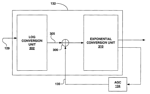
[0033] FIG. 3 is a block diagram illustrating an example embodiment of digital
VGA 132 that operates within the logarithmic domain. As shown, digital VGA
132 includes a logarithmic conversion unit 302 that converts an incoming
linear
baseband signal 129 into a logarithmic domain, such as by converting the
linear
digital values to logarithmic values 305 having units of decibels with a
desired
resolution. In one embodiment, logarithmic conversion unit 302 includes a
logarithmic LUT that maps acceptable values for linear baseband signals to the
logarithmic values. Such a LUT, however, can require significant memory space.
For this reason, various additional techniques are described to reduce the
size of
the logarithmic LUT, and thereby reduce memory space requirements.
[0034] Digital VGA 132 includes an adder 306 rather than a conventional
multiplier. In particular, digital VGA 132 exploits the logarithmic domain,
and
replaces the multiplication function with addition. In other words, digital
VGA
132 exploits the fact that Log (X * Y) = Log (X) + Log (Y), to effectively
replace
a multiplier with adder 306. WCD 100, however, may further process the
amplified baseband signal in the linear domain. Therefore, digital VGA 132 may
also include an exponential conversion unit 310 to convert the baseband signal
back into the linear domain after it has been scaled.
[0035] The gain of digital VGA 132 can be controlled by feedback from AGC
134. In particular, AGC 134 may output a gain value 135 in the logarithmic
domain, such as in units of decibels having the desired resolution. In this
manner, digital VGA 132 need not convert the gain value 135 prior to
application
by adder 306. Rather, digital VGA 132 may amplify or attenuate linear baseband
signal 129 accordingly, simply by adding the gain value 135 to linear baseband
signal 129 in the logarithmic domain.
[0036] Exponential conversion unit 310 converts the scaled baseband signal
from the logarithmic domain back to the linear domain. For example, the
exponential conversion unit 310 may use one or more LUTs, as described in
greater detail below. In addition, the techniques described below may be used
to
CA 02453168 2004-O1-06
WO 03/009129 PCT/US02/22790
9
significantly reduce the size of the one or more exponential LUTs to reduce
memory requirements.
[0037] In one particular case, digital VGA 132 operates in a logarithmic
domain having units of decibels scaled to a desired resolution. As mentioned
above, operating in a logarithmic domain having units of decibels can be
particularly advantageous, because in that case the gain value generated by
AGC
134 can be used without conversion. In other embodiments, however, the
invention may operate in other logarithmic domains or non-linear domains. In
still other embodiments, logarithmic conversion unit 302 and exponential
conversion unit 310 implement algorithms in addition to, or as an alternative
to,
the various LUTs.
[0038] FIG. 4 is a block diagram of one embodiment of digital VGA 132
illustrated in greater detail. In particular, logarithmic conversion unit 302
is
illustrated as including a logarithmic lookup table (LOG LUT) 402. In
addition,
logarithmic conversion unit 302 includes hardware that separates an incoming
signed baseband signal into an unsigned absolute value (ABS as shown at 406)
and a sign bit (as shown at 410). In other words, the sign bit can be removed
from the baseband signal within logarithmic conversion unit 302 and then
propagated and reinserted in exponential conversion unit 310. The logarithm of
a
negative number is undefined. Thus, removing the sign bit from the baseband
signal avoids the scenario where hardware within the digital VGA attempts to
operate on negative numbers within the logarithmic domain. Rather, specific
hardware within digital VGA 132 may operate only on positive numbers within
the logarithmic domain once the sign bit has been removed.
[0039] In one particular example, A/D converter 128 (FIG. 1) produces the
digital baseband signal 129 as an 18-bit binary number, including a sign bit,
7
integer bits, and 10 decimal bits. The sign bit is separated from the baseband
signal and the remaining 17-bit binary number, including 7 integer bits and 10
decimal bits, is fed into LOG LUT 402. As a result of the lookup, the 17-bit
binary number is converted into a 9-bit signed number, which is fed into adder
306. Adder 306 also receives a 9-bit signed number from AGC 134 representing
a gain value in units of decibels with the desired resolution. Notably, the
gain
CA 02453168 2004-O1-06
WO 03/009129 PCT/US02/22790
value is already in the logarithmic domain, and thus requires no adjustment
prior
to input into adder 306. Adder 306 adds the respective inputs to produce a 10-
bit
result, which is fed into exponential conversion unit 310. In one example, a
relatively simple and low cost 9-bit adder is used.
[0040] Exponential conversion unit 310 may include saturation unit 424 and at
least one exponential LUT 428. The saturation unit can be used to saturate the
baseband signal in the logarithmic domain. For example, continuing with the
example above, the 10-bit signed result, which is fed into exponential
conversion
unit 310, can be saturated to 7-bits by saturation unit 424 to span a dynamic
range
represented by 128 possible values. The output of saturation unit 424 is fed
to
exponential LUT 428 along with the sign bit (as shown at 410) to generate a 4-
bit
signed result representing the scaled baseband signal in the linear domain.
Performing saturation prior to the lookup in exponential LUT 430 can save
memory space by reducing the required size of individual entries in
exponential
LUT 430. Moreover, truncation operations can be incorporated into exponential
LUT 430. In other words, any conventional truncation operations that would
need to follow a conventional multiplier type of VGA can be incorporated into
exponential LUT 430 in accordance with the invention simply by defining the
appropriate bit-width of the output of exponential LUT 430.
[0041] FIGS 5A-5C illustrate three different exemplary embodiments of an
exponential conversion unit according to the invention. The saturation unit
424
illustrated in FIG. 4 is not shown in FIGS. 5A-5C, but could be included for
saturation prior to the lookups to reduce the size of one or more LUTs within
the
exponential conversion unit. In addition, entries in the one or more LLITs
within
the exponential conversion unit may have output bit-widths that effectively
truncate digital input signals.
[0042] The exponential conversion unit 502 illustrated in FIG. 5A, includes
different LUTs for positive and negative values. In particular, exponential
conversion unit 502 includes E~ LUT(pos) 506 that stores the 128 possible
positive 3-bit values, and also includes E~ LUT(neg) 510 that stores the 128
possible negative 4-bit values. The sign bit (as shown at 410) is used to
provide
input signal 514 used by multiplexer 518 to select output from the appropriate
CA 02453168 2004-O1-06
WO 03/009129 PCT/US02/22790
11
LLJT. Thus, when the sign bit identifies a negative number, multiplexes 518
selects output from EXP LU'T(neg) 510. When the sign bit identifies a positive
number, multiplexes 518 selects output from EXP_LLJT(pos) 506.
[0043] FIG. 5B illustrates yet another configuration of an exponential
conversion unit. In particular, exponential conversion unit 540, as
illustrated in
FIG. 5B, uses a single EXP_LLTT(pos) 544 and replaces the EXP-LUT(neg) with
an adder 548 that is used to generate the complimentary negative value from a
positive value read from EXP-LUT(pos) 544. For example, given a positive
value X stored in EXP-LUT(pos), the complimentary negative value may be
generated by the appropriate complimentary equation, in one case (-X-1). In
other cases, however, where the negative and positive values are perfectly
symmetric about a Y-axis, the twos-complement equation of -X+1, or the like,
may be used to generate the negative values from the positive values.
[0044] Exponential conversion unit 540, as illustrated in FIG. 5B, can provide
advantages by further reducing memory requirements. In particular, exponential
conversion unit 540 utilizes a single 128-bit by 3-bit LUT, and adder 548.
Exponential conversion unit 502 as illustrated in FIG. 5A, on the other hand,
requires more memory space, but eliminates the additional adder. Each of the
embodiments of FIGS. 5A and 5B has advantages and disadvantages, which can
be considered in determining the best configuration for a given
implementation.
[0045] FIG. 5C illustrates still another configuration of an exponential
conversion unit. Like the embodiment of FIG. 5B, exponential conversion unit
560 illustrated in FIG. 5C uses a single EXP LUT(pos) 544. However,
exponential conversion unit 560 generates negative values by inverting bits
selected from EXP LUT(pos) 544 and appending the sign bit. One's
complement unit 568 can be used to perform the inversion and append unit 574
can be used to append the sign bit after multiplexes 518 selects the desired
output.
The embodiment of FIG. 5C avoids the need for an EXP-LUT(neg) as illustrated
in FIG. 5A and also avoids the need for an adder as illustrated in FIG. 5B.
[0046] FIG. 6 is a block diagram, illustrating in greater detail, one
implementation of logarithmic conversion unit 302. As mentioned above,
logarithmic conversion unit 302 is used to convert digital values of a signal,
e.g.,
CA 02453168 2004-O1-06
WO 03/009129 PCT/US02/22790
12
an incoming linear baseband signal 129, into a logarithmic domain. While
logarithmic conversion unit 302 can be realized by implementing a single LUT
that maps acceptable values for linear baseband signal to the logarithmic
domain,
an alternative configuration, as illustrated in FIG. 6, can significantly
reduce
memory requirements.
[0047] In particular, as illustrated in FIG. 6, logarithmic conversion unit
302
includes various hardware for manipulating a floating point number. For
example, an N-Bit positive binary number X(p) can be expressed as X(p) = m*
2E, where E is referred to as the exponent and represents the position of the
most
significant bit in X(p) that is set to a one, and m is referred to as the
mantissa and
represents the remaining E-1 least significant bits.
[0048] In a logarithmic domain having decibel units, the above floating point
equation can be expressed as:
20.1og(X(p)/ 21°).RdB = 20.1og(2E/ 21°).Ras + 20.1og(m).RdB,
where RdB is the inverse of the desired decibel resolution. The floating point
equation in the logarithmic domain in decibel units can then be expressed as:
X=XE+ Xm,
where XE is the decibel value of the exponent and Xm is the decibel value of
the
mantissa.
[0049] In this particular domain, XE can be stored as a table of N=17 entries,
where each entry is 9-bits wide. Furthermore, Xm can be thought of as N
segments. However, only one of the segments needs to be stored as a table, and
values for all other segments can be derived from entries of the stored
segment.
For example, the m'n segment includes 2m~1 elements, each of which can be
derived from an element of the (m + n)'n segment by left-shifting the input
address of the (m + n)'n segment by n-bits. In addition, a nearest neighbor
interpolation can be performed to derive elements of the (m + n)'h segment
from
elements of the m'n segment. In particular, to interpolate an element of the
(m +
n)'n segment from an element of the m'n segment, the input address of the m'n
segment can be rounded by n-bits and used as the input address of the (m +
n)'n
segment.
CA 02453168 2004-O1-06
WO 03/009129 PCT/US02/22790
13
[0050] Refernng again to FIG. 6, logarithmic conversion unit 302 may include
an exponent extractor 602 and a mantissa extractor 606. An exponent LUT 612
can be used to generate the logarithmic value of the exponent. In addition, a
mantissa LUT 616 can be used to generate the logarithmic value of the
mantissa.
These values can then be combined by adder 620, and possibly truncated by
truncate unit 624.
[0051] In one embodiment, mantissa LUT 616 maps all possible values of the
various mantissa segments. However, to reduce the size of mantissa LUT 616
and thereby reduce memory requirements, address manipulation logic 624 can be
implemented to allow values of one segment of the mantissa to be generated
from
a different segment of the mantissa. In this manner, only a single segment of
the
mantissa can be stored in mantissa LUT 616.
[0052] Address manipulation logic 624 may operate as follows. Assuming that
mantissa LUT 616 includes 2U entries, then
if E > U, let input address M' = round (M/2~E~U~), and
if E S U, let M' _ « (U-E).
In other words, if E > U, then M' is interpolated and defined as the nearest
neighbor input address in the stored mantissa LUT 616, and if E 5 U, M' is
obtained by left shifting the input address by (U-E) bits. M' can then be fed
into
the stored segment to yield the appropriate converted value in the logarithmic
domain.
[0053] FIGS. 7A and 7B are a series of two graphs that further illustrate the
concept behind the embodiment of logarithmic conversion unit 302 illustrated
in
FIG. 6. Again, the floating point equation in the logarithmic domain having
decibel units can be expressed as X = XE + Xm, where XE is the decibel value
of
the exponent and Xm is the decibel value of the mantissa. FIG. 7A is a graph
of
the decibel value of X as a function of linear input, in comparison to a graph
of
the decibel value of XE for the same input. As can be seen in FIG. 7A, the
value
of XE deviates slightly from the value of X at various different inputs.
[0054] FIG. 7B is a graph of the decibel value of Xm. Xm can be viewed as the
variation between X and XE at the various different inputs. Thus, as shown in
FIG. 6, X can be generated from exponent LUT 612 and mantissa LUT 616. In
CA 02453168 2004-O1-06
WO 03/009129 PCT/US02/22790
14
particular, exponential LUT 612 is used to generate the logarithmic value of
the
exponent, and mantissa LUT 616 is used to generate the logarithmic value of
the
mantissa. Importantly, however, to save memory space, mantissa LUT 616 need
only store entries for one of the spikes (i.e. segments) illustrated in FIG.
7A. The
values of the other spikes can then be generated using address manipulation
logic
624 as described above.
[0055] The segment (or spike as illustrated in FIG. 7B) that is stored in
mantissa LI1T 616 can be chosen depending on the level of accuracy required.
For example, the full logarithmic mantissa table can be derived without any
loss
by storing the last segment (in this case the 17'h segment). However, that
would
result in the LUT having 21~-~ = 65,536 entries. Notably, because logarithmic
functions tend to flatten at large inputs, a much smaller segment can be
chosen
without a significant loss in performance in a wireless communication device.
In
particular, experiments have showed that storing the 7'~' segment yields
acceptable approximations for all inputs. This would require a mantissa LUT
having only 2~-' = 64 entries.
[0056] Choosing a relatively small numbered segment for inclusion in the
mantissa table effectively results in non-uniform sampling over the
logarithmic
function. At lower inputs, e.g., in lower segments, where the logarithmic
function changes relatively rapidly, all values in lower numbered segments can
be generated from the larger numbered segment. However, at higher inputs,
where the logarithmic function changes much more slowly, the values are
interpolated from the stored segment. This can be viewed as a sort of non-
uniform sampling of the logarithmic function, wherein at lower inputs more
data
points are preserved, but at higher inputs, fewer data points are preserved.
Experiments have shown that such non-uniform sampling does not result in
significant performance reduction in a WCD.
[0057] To account for any unexpected variables, such as quantization noise,
the
resolution of both exponent LUT 612 and mantissa LUT 616 can be increased by
K-bits to help insure that the data is correct and non-corrupted. Quantization
noise may be introduced whenever a floating point LOG function is represented
by finite bit-width digital numbers. Experiments have showed that increasing
the
CA 02453168 2004-O1-06
WO 03/009129 PCT/US02/22790
resolution of exponent LLJT 612 and mantissa LUT 616 by K = 3 bits can be
sufficient to compensate for quantization noise in a WCD.
[0058] FIG. 8 is a flow diagram illustrating a process that can be used to
reduce
memory requirements when implementing one or more LUTs. The process
illustrated in FIG. 8 may be particularly effective when used in a WCD, but is
not
so limited. For example, the process of FIG. 8 may be used in any computer
device implementing lookup tables.
[0059] As shown, a number is separated into an exponent component and a
mantissa component in a first domain (802). For example, the first domain may
be a linear domain and the number may be binary floating point number
representing digital values of a signal. In that case, the exponent component
can
be extracted from the number simply by identifying and storing the most
significant bit that is set to one. Similarly, the mantissa component can be
extracted from the number simply by storing the remaining least significant
bits.
[0060] The exponent component can be converted from the first domain to a
second domain, such as a non-linear domain (804). Separately, the mantissa
component can be converted from the first domain to the second domain (806).
In one particular case, the second domain is a logarithmic domain having units
of
decibels with the desired resolution. Once converted to the second domain (804
and 806), the exponent and mantissa components can be combined (808). For
example, an adder can be implemented to facilitate the combination simply by
summing the exponent and mantissa components. If desired, the combination can
then be truncated or rounded.
[0061] The conversion of the exponent component can be done using a first
LUT, e.g., an exponent LUT. Similarly, the conversion of the mantissa
component can be done using a second LUT, e.g., a mantissa LUT.
Alternatively, either or both of the conversions may be achieved using an
algorithm, or an algorithm and a LUT in combination.
[0062] The exponent LUT may be relatively small, and may have entries
corresponding to the possible bit positions of the exponent. For example, if
the
number is a 17-bit number, the exponent LUT may have only 17 entries. The
mantissa LUT, on the other hand, may include a much larger number of entries.
CA 02453168 2004-O1-06
WO 03/009129 PCT/US02/22790
16
For example, if the number is a 17-bit number, the mantissa LUT could include
an extremely large number of entries. For this reason, additional techniques
can
be used to further reduce the size of the mantissa LUT, and thus save memory
space.
[0063] FIG. 9 is a flow diagram illustrating a process that can be used to
significantly reduce the size of the mantissa LUT. As shown, only a subset of
a
total number of mantissa values are stored in the mantissa table (902). Values
not
included in the subset can then be derived from the subset (904). In this
manner,
the memory requirements for implementing a mantissa LUT can be reduced.
[0064] Referring again to FIG. 7B, the subset of mantissa values may
correspond to one of the spikes illustrated in FIG. 7B. The values in all of
the
other spikes can be generated either by shifting the input and selecting an
entry in
the subset based on the shifted input, or by interpolating input and selecting
an
entry in the subset based on the interpolated input. If a value in a smaller
numbered mantissa segment is needed (i.e., a segment located to the left of
the
stored segment in FIG. 7B), the shifting operation can be used. If a value in
a
larger number mantissa segment is needed (i.e., a segment located to the right
of
the stored segment in FIG. 7B), the interpolation operation can be used. In
this
manner, the total number of possible mantissa values can be generated, as
needed, from a much smaller subset of mantissa entries stored in a table, thus
saving memory space.
[0065] In particular, if a value in a larger number mantissa segment is
needed,
the input address of that value is interpolated and defined as the nearest
neighbor
input address within the stored mantissa segment. If a value in a smaller
numbered mantissa segment is needed, the input address of that value is left
shifting by a number of bits corresponding to the difference between the
number
of the stored segment and the number of the segment for the desired value. The
interpolated address or shifted address can then be fed into the stored
segment to
yield the appropriate converted value.
[0066] As mentioned above, the particular subset is stored in the mantissa LUT
can be chosen depending on the level of accuracy required. Notably, because
logarithmic functions tend to flatten at large inputs, a small segment can be
used
CA 02453168 2004-O1-06
WO 03/009129 PCT/US02/22790
17
without a significant loss in performance in a wireless communication device.
In
particular, experiments showed that storing the 7'" segment yielded acceptable
approximations for all inputs. This would require a mantissa LUT having only
2~-I = 64 entries.
[0067] In still other embodiments, a somewhat larger mantissa LUT, including
entries that comprise non-uniform sampling of the logarithmic or logarithmic
like
functions can be used. For example, the entries could be pre-computed using
the
techniques described above. In other words, a segment of the mantissa could be
selected and all of the values in smaller segments could be pre-computed and
included within the LUT. However, for larger segments, the entries could be
pre-computed according to the interpolation technique described above. In this
manner, every segment stored within the LUT would have no more entries than
the chosen segment, thus limiting the amount of required memory space.
Although the mantissa LUT would be larger than a LUT storing only the single
segment, the address manipulation logic would not be needed. In designing a
particular implementation, the additional memory space required can be weighed
against the inclusion of address manipulation logic to determine the best, or
most
efficient configuration.
[0068] The various LUTs described above may be stored in memory and
accessed as needed. In some cases, methods described above may be
implemented in software, such as program code. For example, the program code
can be loaded into memory and then executed in a processor. The program code
can be initially carried on computer-readable media such as a hard drive or
magnetic, optical, magneto-optic, phase-change, or other disk or tape media.
Alternatively, the program code may be loaded into memory from electronic
computer-readable media such as EEPROM, or downloaded over a network
connection. If downloaded, the program code may be initially embedded in a
carrier wave or otherwise transmitted on an electromagnetic signal. The
program
code may be embodied as a feature in an application program providing a wide
range of functionality.
[0069] If the invention is implemented in program code, the processor that
executes the program code may take the form of a microprocessor and can be
CA 02453168 2004-O1-06
WO 03/009129 PCT/US02/22790
18
integrated with or form part of a PC, Macintosh, computer workstation,
hand-held data terminal, palm computer, WCD, wireless base station, network
router, or the like. The memory may include random access memory (RAM)
storing program code that is accessed and executed by processor to carry out
the
various method described above.
[0070] Various embodiments of the invention have been described. For
example, a digital VGA has been described for use in a WCD. In particular, the
digital VGA operates within the logarithmic domain, and replaces a
conventional
multiplier and a conventional exponential lookup table having a size greater
than
1000 bytes, with an adder, logarithmic LUTs of nominal size (i.e.
approximately
200 bytes of total space) and a smaller exponential table of nominal size
(i.e.
approximately 128 bytes). Nevertheless, various modifications may be made
without departing from the spirit and scope of the invention. For example,
rather
than implementing lookup tables, the invention could be realized using
algorithms that dynamically convert from logarithmic domains to linear
domains,
and/or vice versa. In addition, the invention could be implemented in other
logarithmic domains. Moreover, the digital VGA according to the invention
could be used in other devices, including, for example, a base station within
a
wireless communication network. For example, any device that implements a
multiplier followed by some sort of truncation may benefit from the invention.
[0071] In addition, aspects of the invention could be used in applications
other
than digital VGA's. For example, any apparatus that performs a multiplication
operation followed by a truncation operation could use aspects of the
invention to
replace a conventional multiplier with an adder. In one case, the invention
can be
implemented to multiply two baseband signals using an adder rather than a
multiplier. In general, the invention can perform multiplication and
truncation by
converting linear digital values to a logarithmic domain, adding the digital
values
in the logarithmic domain and then converting the added value back to a linear
domain. Moreover, a truncation operation can be incorporated into a lookup
table that is used to convert back to the linear domain simply by choosing
output
bit-widths to effectively truncate the signals.
CA 02453168 2004-O1-06
WO 03/009129 PCT/US02/22790
19
[0072] Various techniques for reducing the size of LUTs so as to reduce
memory requirements have also been described. In particular, many of these
techniques have been described in the context of a WCD. However, the
invention is not limited in that respect. For example, the techniques used to
reduce the size of one or more LUTs could also be used in other computer
devices to save memory space. Accordingly, these and other embodiments are
within the scope of the following claims.