Note: Descriptions are shown in the official language in which they were submitted.
CA 02453229 2003-12-12
WH-11 724CA
TITLE: REFLECTIVE OPTICAL SENSOR FOR BILL VALIDATOR
FIELD OF THE INVENTION
The present invention relates to bill validators,
having an optical sensor means for measuring the
reflectance and transmittance of paper bills as they move
past the optical sensor. The sensor includes a radiation
emitter which also acts to direct reflected radiation to
a photodetector. This sensor may also be used as common
reflective sensor for detection of various index marks
with relatively small space dependence.
BACKGROUND OF THE INVENTION
Bill validators used in vending machines and the
like typically utilize various styles of reflective
optical sensors to obtain measurements from an inserted
bill to determine authenticity, denomination and
location. Typically, the bill is transported past at
least one photosensor, having a light-emitting diode
(LED) and photodetector (photodiode or phototransistor).
Some factors that adversely affect the bill
measurements include the following: inserted bills are of
different denominations, cleanliness and quality; bill
may be creased or crumpled, and the bill location and
inclination across passageway may strongly vary. In
addition, the output power of LED can vary due to age
and/or ambient conditions. Furthermore, there are normal
production variations in LED optical power output and
detector sensitivity, which can lead to sensors having
varying current and voltage requirements in order to
operate effectively. In order to partially offset these
factors, optical sensor measurements are taken over a
large dynamic range. As power of LED and sensitivity of
- 1 -
CA 02453229 2003-12-12
WH-11 724CA
photodetector are limited, the optical efficiency should
be high to improve the performance of the sensors.
In the art, many embodiments of reflective optical
sensors are known. The simple sensors comprise at least
one photo emitter and one photo detector with relatively
wide spatial diagrams (U. S. Patent 4,348,656; U.S. Patent
4,628,194; U.S. Patent 5.222.584; U.S. Patent 5,476,169;
U.S. Patent 5,692,067; U.S. Patent 5,751,840; U.S. Patent
S,8S5,268; U.S. Patent 5,889,883; U.S. Patent 5,909,503;
U.S. Patent 5,960,103). Such sensors have low optical
efficiency and their output signal strongly depends on
bill location and inclination across passageway. The
space required to mount the sensors (footprint) slightly
exceeds the total area of the emitters and detectors.
To improve optical efficiency, many sensors mount
the emitters and detectors at an angle to one another and
converging on the bill surface (U. S. Patent 4,041,456;
U.S. Patent 4,628,194; U.S. Patent 4,973,851; U.S. Patent
5,420,406; U.S. Patent 5,467,405; U.S. Patent 5,483,069;
U.S. Patent 5,918,960; U.S. Patent 5,992,601; U.S. Patent
6,028,951; U.S. Patent 6,073,744). These sensors require
special optical heads, receptacles etc. The footprint for
these sensors significantly exceeds the total area of
emitters and detectors due to the various mounting and
carrying paths. Even with this more complicated design,
the output signal from these sensors strongly depends on
bill location and inclination across passageway.
Advanced sensors in addition to plurality of LED's
and photo detectors comprise various focusing, light
guiding and reflecting elements, including fiber optic
"fish tails" and splitters (U. S, Patent 5,308,992; U.S.
Patent 5,381,019; U.S. Patent 5,616,915; U.S. Patent
- 2 -
CA 02453229 2003-12-12
WH-11 724CA
6,044,952; U.S. Patent 6,104,036; U.S. Patent 6,163,036;
U.S. Patent 6,188,080; U.S. Patent 6,359,287; U.S. Patent
6,392,863). These sensors are more complicated, large and
expensive, require special optical parts and often
require additional alignment during validator assembly.
The output signal of these advanced sensors continues to
be largely dependent on bill location and inclination
across passageway.
Some special optical sensors conduct bill scanning
by means of LED's and detectors arrays with special
lenses or by direct TV image or light beam scanning (U. S.
Patent 4,179,685; U.S. Patent 4,197,584; U.S. Patent
4,293,776; U.S. Patent 6,363,164). This technology is
expensive and is not suitable for mass production and
utilization.
Some optical shadow on a bill may occur with the
majority of prior art sensors because of bill
inclination, illumination or observation.
It is a general object of the present invention to
provide a simple reflective space efficient sensor having
high optical efficiency for bill examination and other
applications.
The present invention overcomes a number of the
disadvantages described above with respect to the prior
art sensors.
SUMMARY OF THE INVENTION
A validation device for sensing the authenticity
of bills according to the present invention comprises a
bill passageway, an optical sensing arrangement to one
side of the passageway and opening onto the passageway
- 3 -
CA 02453229 2003-12-12
WH-11 724CA
for directing radiation onto a bill as it moves past the
sensor and for receiving radiation reflected from the
bill; an arrangement for processing an output signal of
the optical sensing arrangement produces an eluation
signal. An evaluation system uses the evaluation signal
and based thereon, makes a prediction of the authenticity
of the bill. The optical sensing arrangement includes a
bulb emitter encased in a case transparent to luminous
radiation and at least one photodetector is situated to
receive radiation emitted by the bulb emitter and
reflected by a bill and returned to the photodetector by
passing through the plastic case of the bulb emitter.
According to an aspect of the invention, the bulb
emitter is a light emitting diode device preferably with
a plastic case.
According to yet a further aspect of the
invention, the case of the light emitting diode device
includes a convex end which faces the bill passageway and
acts as a lens to direct emitted radiation onto the bill
and to receive and direct radiation impinging on the
convex lens through the case to the photodetector.
In yet a further aspect of the invention, the
plastic case has a generally flat transparent base
adjacent the photodetector and the photodetector is
located below the base.
In yet a further aspect of the invention, the
convex end of the case is immediately adjacent the bill
passageway.
In yet a further aspect of the invention, the
convex end of the case is of a width greater than the
spacing between the convex end and the center line of the
bill passageway.
- 4 -
CA 02453229 2003-12-12
WH-11 724CA
In yet a further aspect of the invention, the case
acts as a light guide for focusing radiation emitted by
the bulb emitter and reflected from the bill onto the
photodetector.
In yet a further aspect of the invention, the
light emitting diode is a directional emitter directing
emitted radiation generally through the convex end of the
case.
In yet a further aspect of the invention, the
light emitting diode is designed to emit ultraviolet
radiation.
In yet a further aspect of the invention, a
validation device comprises the ultraviolet absorbing
thin film filter between light emitting diode base and
photo detector.
In yet a further aspect of the invention, the
opposite to light emitting diode part of outlying
passageway wall is made from white non luminescent
material.
In yet a further aspect of the invention, the
optical sensor includes white light emitting diode and at
least two photo detectors with band-pass or rejection
colored thin film filters between light emitting diode
base and said photo detectors.
In yet a further aspect of the invention, the
optical sensor includes multicolor mufti chip light
emitting diode with at least one photo detector adjacent
to light emitting diode base.
In yet a further aspect of the invention, optical
sensor includes the opaque cap round said light emitting
- 5 -
CA 02453229 2003-12-12
WH-11 724CA
diode with end slit for bar-code reading and bill edge
detection.
Additionally in accordance with preferred
embodiment of the present invention, there is provided a
method of bill ultraviolet examination including
perpendicular narrow-beam illumination of a portion of a
bill surface by means of a transparent body bulb
ultraviolet light emitting diode, and collection of the
mirror and diffuse reflected ultraviolet light and
fluorescent light from the illuminated bill portion by
light emitting diode convex end, and transmission of this
collected light throw transparent light emitting diode
body to at least one photo detector adjacent to said
light emitting diode base and filtering of said
transmitted light with an ultraviolet absorption filter
between said light emitting diode base and detector, and
detection of transmitted light with planar PIN photo
diodes, and processing of output photo signal for bill
identification and validation.
Also provided, in accordance with preferred
embodiment of the present invention, is a method for
simultaneous evaluation of optical characteristics of a
bill including perpendicular narrow-beam illumination of
part of a bill surface by means of a white light emitting
diode with a transparent bulb body having a convex end,
and collection of the mirror and diffuse reflected light
from the illuminated bill part using the convex end of
the light emitting diode, and transmission of collected
light through the transparent light emitting diode body
to photo detectors adjacent to a base of the light
emitting diode and filtering of transmitted light with
absorption and/or bend-pass filters, and detection with
planar PIN-photodiodes, and separate processing of steady
- 6 -
CA 02453229 2003-12-12
WH-11 724CA
and alternate photo signal components from each photo
detector for bill identification and validation.
Further provided, in accordance with preferred
embodiment of the present invention, is a method for
sequential evaluation of optical characteristics of a
bill including: sequential perpendicular narrow-beam
illumination of part of a bill surface with varicolored
light by means of a transparent body bulb multi color
mufti chip light emitting diode, and collection of mirror
and diffuse reflected light from the illuminated bill
part by means of a convex end of the light emitting
diode, and transmission of collected light through the
transparent body of the light emitting diode to a photo
detector adjacent to a base of the light emitting diode,
and sequential detection and processing of said
varicolored light components for bill identification and
validation.
Additionally provided, in accordance with
preferred embodiment of the present invention, is method
for bar code reading and bill edge detection including
perpendicular narrow-beam illumination of separate bar or
bill edge throw slit in opaque light emitting diode cap,
and collection of the mirror and diffuse reflected light
from illuminated surface throw said slit by means of
light emitting diode convex end, and transmission of the
collected light throw transparent light emitting diode
body to photo detector adjacent to light emitting diode
base, and detection of transmitted light with planar
photo detector, and processing of alternate photo signal
component from photo detector for bar code identification
and bill edge location.
CA 02453229 2003-12-12
WH-11 724CA
In operation light emitting diode with narrow
diagram is positioned perpendicularly and in close
proximity to the bill surface to illuminate part thereof.
The illuminated part of the bill surface is practically
equal to from the size of the light beam emitted from the
light emitting diode. The power of the light reflected
back in a particular direction is proportional to the
degree of specularity and the diffuse behavior of the
bill surface. Bills contain both specular and diffuse
surfaces as part of their design and material properties
with the main surface being predominantly diffuse. Use of
highly reflective devices such as plastic blazed
holograms, metallized labels and threads creates areas of
specular reflection. Additionally, the bill (substrate
or/and dye) often emits fluorescent light of a certain
wavelength (or several wavelengths) when irradiated with
ultraviolet light. To obtain good optical information
about the bill under investigation, all light components
outgoing from the illuminated bill surface should be
collected. Under perpendicular illumination specular
reflected light propagates in exactly opposite direction.
Diffuse and fluorescent components propagate more
uniformly (in general according to so-called cosine law).
Due to small gap between the light emitting diode and the
bill, most of the outgoing light from the illuminated
bill surface is collected with the convex end of the
light emitting diode and is transmitted to the photo
detector through the transparent light emitting diode
body. With this arrangement, the light emitting diode
body is used as a total reflection light guide and
collector without any additional optical parts. Such an
arrangement has low sensitivity to bill vibration and
inclination in the passageway at inclination angles up to
the maximum light emitting diode beam aperture (commonly
8 - 12°) by reason of insignificant variations of
- g _
CA 02453229 2003-12-12
WH-11 724CA
perpendicular to bill light power within this angle
aperture. Additionally, due to the narrow light emitting
diode aperture, ambient light-striking the bill surface
is also insignificant for bill testing.
Transmitted light through the light emitting diode
body is detected with broad band and selective photo
detectors situated under the transparent light emitting
diode base. Low-cost thin film band-pass or absorption
rejection filters are used in conjunction with
hardware/software subtraction provides an integrated
intensity and separate color (including ultraviolet
reflection) signals from the bill under investigation.
Using an opaque cap round light emitting diode
with an end slit in conjunction with its narrow diagram
and alternate signal component processing provides stable
contrast signal under bar-code reading and bill edge
detection.
Several embodiments of the present invention will
now be described by way of example with reference to the
accompanying drawings.
BRIEF DESCRIPTION OF THE DRAWINGS
Preferred embodiments of the invention are shown
in the drawings, wherein:
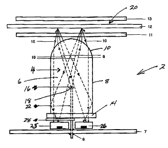
FIG 1 is an enlarged side view of optical sensor
for bill ultraviolet testing;
FIG. 2 is an exploded enlarged perspective
assembly view of optical sensor for bar-code reading and
bill edge detection;
FIG.3 is a block diagram of hardware component
processing of signals in ultraviolet optical sensor;
- 9 -
CA 02453229 2003-12-12
WH-11 724CA
FIG. 4 is a typical signal of genuine bill
ultraviolet scanning in FIGURE 1 embodiment;
FIG. 5 is a typical signal of counterfeit bill
ultraviolet scanning in FIGURE 1 embodiment; and
FIG. 6 is a typical signal of bar code scanning in
FIGURE 2 embodiment.
DETAILED DESCRIPTION OF THE PREFERRED EMBODIMENTS
The optical sensor 2 shown in Figure 1 is
positioned for emitting radiation to eradiate the bill
12. The surface characteristics of the bill alter the
radiation which is reflected from the bill and returned
to the optical sensor. The bill 12 is transported
through the bill passageway 20 defined by an exterior
wall 13 and a light transparent wall 11.
The optical sensor 2 has a light emitting diode
(LED) 4, positioned to one side of the passageway 20 and
located immediately adjacent the transparent wall 11.
The light emitting diode 4 has a transparent case 6 with
a generally cylindrical portion terminating at one end in
the convex lens portion 10 and closed at the other end by
the quasi planar base 14. The case 6 is preferably of a
plastic or other light transmitting material. Radiation
produced by the LED 4 passes through the plastic case.
Generally centered within the case is a luminous chip 16
centrally located in a non light transmitting concave
recess 18. The luminous chip 16 is connected by a pair
of leads 22 to a power source. Radiation from the
luminous chip 16 generally passes in a parallel manner
through the convex lens 10 of the plastic case 6. The
radiation produced by the LED is generally through the
end of the LED and produces a narrow beam of radiation
for eradiating the bill 12. The radiation produced by
the LED strikes the bill and depending upon the
characteristics of the bill, is reflected from the
surface thereof. A portion of this reflected radiation
- 10 -
CA 02453229 2003-12-12
WH-11 724CA
strikes the convex lens 10 of the LED and passes
therethrough and is guided to the base 14 of the LED and
through the base to photodetectors 25 and 26 located
exterior to the based of the LED.
From the above, it can be appreciated that the
casing of the LED acts as a light guide for directing
reflected radiation from the bill, which strikes the
convex end of the plastic case of the LED to the
photodetectors located below and outside of the LED.
Both the LED 4 and the photodetectors 25 and 26 are
mounted on the printed circuit board 7 and the signals
from the photodetectors are processed by circuitry on the
printed circuit board.
The diameter of the cylindrical walls 8 of the LED
are of the order of 5 mm and the radiation produced by
the LED is generally of this width and it is generally
directed in a perpendicular manner towards the surface of
the bill 12. The bill 12 is spaced from the convex end
10 of the LED up to approximately 3.5 mm. It can thus be
appreciated that the beam of radiation is wide relative
to the distance of separation from the LED to the bill.
The convex end 10 serves to focus reflected radiation
back onto the photo diodes 25 and 26. With this
arrangement, most of the outgoing radiation which serves
to illuminate the bill surface and is reflected
therefrom, is collected by the LED convex lens and
transmitted to the photodetectors. It has generally been
found that this arrangement results in a reflected signal
which is maintained within a much tighter tolerance even
with changes in location of the bill in the passageway,
the condition of the bill and the inclination thereof.
It has been found that the reflected signal is
typically in the range of 60% to 85°s of the produced
signal. Thus the optical signal would change up to
approximately 30% under bill displacement across the
- 11 -
CA 02453229 2003-12-12
WH-11 724CA
passageway of up to 2 mm. The beam of radiation produced
by the LED is relatively narrow, typically between 8 and
12 degrees. The close positioning of the LED to the bill
and the use of the LED as a wave guide to return the
reflected radiation, results in a signal which is less
sensitive to bill inclination in the passageway.
The embodiment shown in Figure 1 also includes a
filter arrangement 28 between the base 14 and the
photodetector 25. This preferably is an ultraviolet
absorbing film filter. With this arrangement, the LED is
preferably a 5 mm bulb ultraviolet LED under the
trademark HUUV-5102L sold by Roithner Lasertechnic or
general equivalent. Thus the bill 12 is exposed to
ultraviolet radiation with the reflected signal and any
luminous signals of the bill returning through the LED to
the photodetectors 25 and 26. Photodetector 26 receives
the entire signal whereas the signal received by
photodetector 25 is absent any ultraviolet portion.
The embodiment of Figure 1 produces a signal at
photodetector 26 which is a result of all light radiation
striking the detector. In contrast, photodetector 25 is
a similar signal but with the W component removed.
Ambient light can also influence photodetectors, however,
the positioning of the photodetectors beneath the LED and
the plastic casing of the LED acting as a light
transmitting guide to the photodetectors, reduces
problems associated with ambient light. Furthermore,
ambient light is generally associated with the bill
passageway 20 and the structure of the optical sensor
locates the photodetectors, a significant distance away
from the passageway. In this way, the photodetectors are
not as sensitive to ambient light in the passageway.
Optical sensor 2 is located in its own casing having
its own transparent wall 11 which forms part of the
passageway. This forms a module with the printed circuit
- 12 -
CA 02453229 2003-12-12
WH-11 724CA
board and the LED located within a housing typically
formed of a non transparent plastic with the exception of
the transparent wall 11. The elongate form of the
optical sensor advantageously uses the LED to not only
produce radiation for illuminating the bill but it also
uses the LED as a light guide for directing the reflected
radiation to the photodetectors located beneath the LED.
Opposite passageway wall 13 is made from white non
fluorescent ABS plastic. Reflection signal from this wall
is used for apparatus self calibration when bill is
absent in passageway.
Figure 2 is a perspective view of an alternate
embodiment of the optical sensor. The optical sensor 100
is positioned adjacent the transparent wall 110 in the
bill passageway 120 having an exterior wall 113. The
bill 112 or other document is shown having a bar code
115. The optical sensor 100 includes a printed circuit
board 107 having a photodetector 105 mounted thereon.
The photodetector 105 is exposed to the reflected
radiation which will pass back through the LED 101. This
LED has a transparent outer casing 104 made up of a
cylindrical portion 106, a convex end portion 108, and a
generally planar transparent base 109. The LED includes
its own light source 111 within the LED which is designed
to direct radiation out through the convex end 108.
Connectors 130 and 132 support the light source 111
generally centered within the LED and connected and
provides power to it from the printed circuit board 107.
A non transparent shield 140 covers the end of the
LED and has a slit opening 150 for allowing the radiation
to pass therethrough. As can be appreciated, some of the
radiation will be reflected off the end wall 142 of the
end cap, however, this will be a constant signal back to
the photodetector 105 where various arrangements can be
- 13 -
CA 02453229 2003-12-12
WH-11 724CA
used to reduce this radiation component. A portion of
the produced radiation will pass through the slot 150 and
will provide a narrow radiation source for illuminating
the individual bars of the bar code 115 as they pass by
the optical sensor. The signal which is returned to the
photodetector through the LED 104 acting as a wave guide
and through the transparent base 109 to the photodetector
will vary in accordance with the bar code 115. This
arrangement has proven to provide a very effective means
for reading of the bar code and providing good quality
results with the various possible misorientations of the
bar code within the passageway 120. As can be
appreciated, the optical sensor 100 and the transparent
wall 110 can be integrated into a single module which is
inserted in a suitable port in the wall of the bill
passageway of a validator or other sensing device.
The arrangement of Figure 2 is also effective in
identifying a bill edge. This is particularly useful for
detecting a leading or trailing edge of a bill as it
moves past the sensor.
With the embodiment of Figure 2, the beam of light
eradiating the bill has a small angle of divergence so
the light divergence on the bill surface does not exceed
0.3 mm. A red LED LTL2F3VEKNT by LITE-ON Inc. and IC
photo detector 57184 or 57815 by HAMAMATSU Co. can be
used in the bar-code detector.
Figure 3 is a block diagram of hardware components
used to process signals in an ultraviolet optical sensor.
Light 10 reflected from the bill surface is received by
photodiode 6 (integral light detector) and is received by
photodiode 5 (detector of visible light) after passing
through Uv absorbing filter 4. Signal Uinc, proportional
to visible light intensity, proceeds from the output 20
- 14 -
CA 02453229 2003-12-12
WH-11 724CA
of amplifier 17. This signal describes the fluorescent
properties of the bill paper and dyes. Signal -(Uint +
UW), proportional to total light outgoing from bill,
proceeds from the output of amplifier 18 to resistor
adder 19. Under equal transfer constants of amplifiers
17, 18 and resistors R in adder unit 19 at the output 21,
outgoing signal 1J2[Uint- (Uint + Uw) ~ _ -1/2 U~, is
developed. This signal describes the ultraviolet
reflection of bill surface. Signals from outputs 20, 21
are used in a processor module for bill authorization and
'discrimination. For example, a large value of Uint signal
indicates that bill may be counterfeit - i.e. a photocopy
on a wood-based paper.
Figure 4 is a typical signal Uinr, of genuine bill
ultraviolet scanning in Figure 1 embodiment. Scanning
speed is about 300 mm/sec. Point 22 indicates the moment
of bill leading edge passing by optical sensor. Point 23
indicates the moment of bill trailing edge passing by
optical sensor. The signal at 24 (bill is absent in
passageway) is caused by back wall 13 reflectance of blue
components of illuminating light and by light reflected
from all transparent interfaces (about 6% on each) -
boundaries between LED and air, air and wall 11, wall 11
and air. The signal at 24 is used for apparatus self
calibration. Signal Uint between points 22 and 23 is
caused by bill paper and dyes fluorescence and
reflectance of blue components of illuminating light.
Figure 5 is a typical signal Uint of a counterfeit
bill (similar to previous genuine bill) ultraviolet
scanning in Figure 1 embodiment. Scanning speed is about
300 mm/sec. Points 22 - 24 indicate the same as in
previous illustration. Bands 25 indicate strong
- 15 -
CA 02453229 2003-12-12
WH-11 724CA
fluorescence from leading and trailing bill borders. Band
26 indicates the strong fluorescence from paper bill
surface in the watermark zone. Signal Uint strongly
differs on genuine and counterfeit bills and is easily
used in the processor module to identify counterfeit
bills.
Figure 6 is a typical signal of bar code scanning
in Figure 2 embodiment. The slit 15 in opaque cap 14 is
5 mm length and 0.4 mm wide. Scanning speed is about 300
mm/sec. This arrangement provides a good spatial
resolution with bar distance and width less then 0.5 mm.
The present invention is described herein in the
context of a banknote application used in a verification
device, automatic cash machine or other bills handling
device, in a bank, postal facility, supermarket, casino
or transportation facility. However, it is appreciated
that the embodiments shown and described herein may also
be useful for checking other objects, particularly flat
objects, such as cards, films, paper sheets and
paintings. The checking device may be stationary or
portable, battery powered or powered by connection to an
electric outlet.
It is appreciated that various features of the
invention, which are, for clarity, described in the
contexts of separate embodiments, may also be provided in
combination in a single embodiment. Conversely, various
features of the invention which are, for brevity,
described in the context of a single embodiment, may also
be provided separately or in any suitable combination.
- 16 -
CA 02453229 2003-12-12
WH-11 724CA
Although various preferred embodiments of the
present invention have been described herein in detail,
it will be appreciated by those skilled in the art, that
variations may be made thereto without departing from the
spirit of the invention or the scope of the appended
claims.
- 17 -