Note: Descriptions are shown in the official language in which they were submitted.
CA 02453336 2004-O1-08
WO 03/015218 PCT/US02/24790
BATCH ELECTRICALLY CONNECTING SHEET
Technical Field
The present invention relates to a heat curable conductive adhesive sheet
used when a wiring pattern or the like of an electric circuit is connected,
particularly to a batch electrically connecting sheet for connecting plural
contact
points of a wiring pattern of an electric circuit electrically in a batch
manner.
Description of the Related Art
When making electric connections of large-current circuits, grounding of
printed wiring boards, connection of battery electrodes, and electric
connection of
microwave printed wiring boards to heat sinks, housings or the like, it is
necessary
that the connections be mechanically, thermally and electrically stable.
In recent years, electronic parts on which electronic circuits integrated at a
high density are mounted are used as electronic apparatus continue to be made
smaller and lighter. Usually, electronic circuits control electronic
apparatus, using
high-frequency signals. High frequency signals are easily affected external
minute
noises, and the signals may result in malfunction of electronic apparatus. To
remove such noises, it is necessary to perform shielding, grounding or the
like. It
is required to form electric connection having a low resistance easily and
surely.
Several conductive materials suitable for connecting a wiring pattern or
other electric circuits are suggested. However, considering the tendency to
make
electronic apparatus smaller and lighter in size, typical examples thereof are
conductive adhesive agents and metal foil tapes.
Japanese Patent Laid-Open Publication No.Hl(1989)-113480 and Japanese
Patent Laid-Open Publication No.Hl(1989)-309206 disclose conductive adhesive
agents wherein conductive particles are dispersed in a heat curable resin. The
conductive adhesive agents cause the conductive particles in the heat curable
resin
to contact each other by heat-curing the adhesive agent under pressure of the
heat
curable resin, to give electric conductivity. The contact between the
conductive
particles is in general a point-contact, i.e., the conductive particles are
electrically
connected to each other in a very small contact area. The conductivity of the
conductive adhesive agents in such a case is easily affected by environmental
-1-
CA 02453336 2004-O1-08
WO 03/015218 PCT/US02/24790
changes, and is therefore poor in stability. It is also difficult to heat-cure
the agents
under pressure, using only simple equipment such as an ordinary oven. A
special
tool for pressing contact points upon the heat-curing is necessary, and the
execution step is complicated.
Further, when a large electric current is sent thereto, heat may be generated
at portions of contact points since there is a large contact resistance. When
specific
conductive particles, namely metal plated macromolecular particles, are used,
the
contact area can be made larger to some extent. However, the conductive layer
is
very thin; therefore, the problem of heat-generation may still exist. For
example,
when a large electric power of 100 W or more is continuously applied to an
electric
connection based on such a conductive adhesive agent, Joule heat is generated
to
such a degree that it negatively effects surrounding electronic parts.
On the other hand, the metal foil tape is a conductive pressure-sensitive
adhesive sheet composed basically of a metal foil and a pressure-sensitive
adhesive
layer. In the case of an embossed metal foil tape wherein hollow projections
are
fitted to a metal foil tape by an embossing process, the hollow projections
break
through the pressure-sensitive adhesive layer to contact an object to be
adhered
electrically and directly. By deformation of the hollow projections, a
relatively
large contact area can be ensured. As a result, the conductivity of the metal
foil
tape is more stable than that of the conductive adhesive agent.
However, in the case of the metal foil tape, the pressure-sensitive adhesive
layer is generally made of an acrylic pressure-sensitive adhesive agent and
has
poor adhesion at elevated temperatures and limited heat resistance. When a
large
electric current is sent thereto, the layer may be easily stripped from the
object to
be adhered by Joule heat. Thus, the thermal stability and the mechanical
strength
of connection are poor.
Thus, the electrical connection for sending a large electric current must rely
on a mechanical caulk, as disclosed in Japanese Patent Publication H7(1995)-
16090, or welding. Complicated operation is required for execution.
Furthermore,
when plural contact points are formed, it is necessary that connecting
operation is
performed for each of the contact points. A great deal of labor is required.
-2-
CA 02453336 2004-O1-08
WO 03/015218 PCT/US02/24790
The present invention is an invention for solving the above-mentioned
problems. An object thereof is to provide a batch electrically connecting
sheet
which makes it possible to form a low-resistance electric connection with
mechanical, thermal and electrical stability at plural points of contact by a
simple
procedure.
Summary of the Invention
The present invention is a batch electrically connecting sheet comprising a
heat-resistant sheet having plural perforations, conductive blocks, inserted
in the
perforations having ridges including indentations and projections outstanding
from
the perforations. The conductive blocks are thicker than the heat-resistant
sheet,
and an adhesive layer composed of a heat curable adhesive agent applied on at
least one surface of the heat-resistant sheet, the surface covering the
projections of
the conductive blocks.
The term "batch electrically connecting sheet" means a sheet which
electrically connects at multiple points.
Brief Description of the Drawings
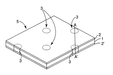
Fig. 1 is a perspective view illustrating an example of the batch electrically
connecting sheet of the present invention.
Fig. 2 is an AA' sectional view of the batch electrically connecting sheet of
Fig. 1.
Fig. 3 is a sectional view illustrating an example of the batch electrically
connecting sheet of the present invention.
Fig. 4 is a sectional view of a connecting structure made of the batch
electrically connecting sheet of the present invention.
Figs. 5a and Sb are process drawings which schematically illustrate a
process of forming an electric connection from the batch electrically
connecting
sheet of the present invention.
Fig. 6 is a sectional view of a connecting structure made of the batch
electrically connecting sheet of the present invention.
Fig. 7 is a sectional view of a connecting structure made of the batch
electrically connecting sheet of the present invention.
-3-
CA 02453336 2004-O1-08
WO 03/015218 PCT/US02/24790
Fig. 8 is a plan view of an example of the embodiment wherein a batch
electrically connecting sheet of the present invention is used to perform
batch
electric connection.
Description of Reference Numerals
1 ... heat-resistant sheet,
2, 2' ... adhesive layer,
3 ... conductive block,
4, 4' ... projections,
5 ... batch electrically connecting sheet,
6, 6' ... conductive object to be adhered.
Detailed Description of the Invention
The present invention will be described according to preferred
embodiments. In the drawings, the same reference numbers are attached to the
same parts or the corresponding parts.
Fig. 1 is a perspective view illustrating an example of the batch electrically
connecting sheet of the present invention. Correspondingly to the positions of
contact points of a conductive object to be adhered, plural conductive blocks
3 are
formed. The arrangement of the conductive blocks 3 may be regular or
irregular.
Fig. 2 is an AA' sectional view of the batch electrically connecting sheet.
This batch electrically connecting sheet 5 has a heat-resistant sheet 1, an
adhesive layer 2 applied on the front surface of the heat-resistant sheet 1,
and an
adhesive layer 2' applied on the rear surface of the heat-resistant sheet. In
the heat-
resistant sheet, perforations are made correspondingly to the positions of
contact
points of an object to be adhered. Conductive blocks 3 are inserted into the
perforations. The conductive blocks 3, are thicker than the heat-resistant
sheet
used so that the blocks can contact the contact points of the object to be
adhered
when the blocks are subsequently sandwiched between the objects to be adhered
and then adhered to the objects under pressure. At this time, it is preferred
that the
blocks 3 have ridges constituting indentations and projections 4 which
protrude
from the front surface and the rear surface so that the blocks can easily
pierce the
adhesive layer to contact the object to be adhered.
-4-
CA 02453336 2004-O1-08
WO 03/015218 PCT/US02/24790
The heat-resistant sheet should be formed from a material having strength,
flexibility, and heat resistance having such a degree that can resist the
curing
temperature of the heat curable adhesive agent. In general, a film of a heat
resistance polymer is preferably used as the heat-resistant sheet.
Particularly
preferred examples of the polymer include polyimide, polyester, polyphenylene
ether, polyether imide, polyarylate, polyether sulfone, and polyphenylene
sulfide.
The thickness of the heat-resistant sheet is not particularly limited, and is
usually from 1 to 2000 Vim, preferably from 10 to 1000 Vim, and more
preferably
from 20 to 100 Vim. If this heat-resistant sheet has a thickness of less than
about
1 Vim, the insulating reliability of insulated portions is poor. If the sheet
has a
thickness of more than about 2000 Vim, flexibility becomes poor so that
handling
becomes inconvenient.
The perforations in the heat-resistant sheet can be manufactured by
punching the sheet, or by other means such as laser ablation. One or more
perforations) may be formed in the sheet. The planar shape of the perforations
is
usually circular, but is not particularly limited. If necessary, the shape may
be
polygonal, linear, curved or the like. The size of the perforations may be
decided
dependently on the size of the conductive object to be adhered, and is not
particularly limited. Usually, about the size of the perforations, the
perforation
diameter is from 0.01 to 10 mm, preferably from 0.1 to 5 mm.
The material of the conductive blocks inserted into the perforations is not
particularly limited. However, considering thermal conductivity as well as
electric
conductivity, a preferred conductive block is made of iron, stainless steel,
silver,
aluminum, nickel, tin or copper. Copper, iron and aluminum are particularly
preferred due to cost considerations. The conductive block may be subjected to
plating made of gold, tin, solder, silver, zinc, nickel or the like.
The planar shape of the conductive block is usually made to a shape
corresponding to the perforations. The thickness of the conductive blocks,
which
includes that of the projections present in the ridges, is about 105 to 200%,
preferably about 110 to 150% of the thickness of the heat-resistant sheet. If
the
thickness of the conductive block is less than 104% of that of the heat-
resistant
sheet, the contact between the conductive block and the contact point of the
-5-
CA 02453336 2004-O1-08
WO 03/015218 PCT/US02/24790
conductive object to be adhered becomes incomplete. If the thickness is more
than
300%, the conductive blocks may not insert well in the heat-resistant sheet.
The conductive blocks have a ridged surface including projections 4 and 4',
formed in both the front surface and the rear surface of the conductive block,
respectively. The shape of these projections 4 and 4' is not particularly
limited.
The projections may be in a conical, pillar, mesa form or a lattice form to
protrude
partially. Alternatively, the front surface and the rear surface of the
conductive
blocks may undulate to form indentations and projections 4 and 4'.
The number of the projections formed on the surface of the conductive
blocks is not particularly limited, and is generally from 1 to 1000 per mmz,
and
preferably from 10 to 1000 per mm2.
The size of the projections, i.e., the height is from 1 to 2000 ~m and the
average diameter thereof is from 10 to 20000 Vim. If the height or the average
diameter is below the lower limit thereof, the surface of the conductive
object to be
adhered and the difference between the projections become similar so that
contact
trends to be unstable. If the height and the average diameter are over the
upper
limit thereof, great pressure is required for crushing the projections at the
time of
connection. Considering the case in which an ordinary conductive object to be
adhered is used to use a press machine of 1 ton or less, preferred height and
average diameter are from 10 to 200 ~m and from 100 to 5000 Vim, respectively.
Particularly in the case in which the conductive object to be adhered is a
high-frequency printed board such as a microwave printed wiring board, the
average diameter of the projections is preferably set to not more than 1/2 of
the
wavelength of the above-mentioned high-frequency. If the interval between the
projections is over 1/2 of the above-mentioned high-frequency, a conductive
area
surrounding non-contact portions functions as an antenna so that a risk of
causing
noises may be generated.
Metal materials are generally superior in malleability and ductility, and can
easily be processed into a sheet form. About metals, the surface thereof is
easily
ridged or undulated by an embossing process. Accordingly, in the case in which
metal is used as the conductive blocks, the conductive blocks are easily
formed by
-6-
CA 02453336 2004-O1-08
WO 03/015218 PCT/US02/24790
punching out a metal sheet into a shape corresponding to the perforations and
subsequently the surface thereof is subjected to an embossing process.
Considering that sufficient adhesive strength is obtained and
simultaneously the contact between the heat-resistant sheet 1 and the
conductive
object to be adhered (non-illustrated) is made easy, the adhesive layers 2 and
2'
usually have a thickness of 1 to 100 Vim, preferably from 5 to 50 Vim, and
more
preferably from 10 to 40 ~m , and are arranged on both surfaces of the heat-
resistant sheet 1.
The adhesive layer is formed from a heat curable adhesive agent. A
preferred example of the heat curable adhesive layer is formed from a heat
curable
resin composition containing the following components:
(1) epoxy resin,
(2) a curing agent for the epoxy resin, and
(3) phenoxy resin.
The heat curable adhesive agent does not have tackiness substantially.
The epoxy resin reacts with the curing agent at a raised temperature or
ambient temperature, so as to make it possible to form a cured product having
a
three-dimensional network structure. In this case, the cured product of the
epoxy
resin is superior in heat resistance and the like, and gives cohesive power to
the
adhesive layer so that objects to be adhered can be adhered to each other. As
a
result, the adhesive layer, which is different from the metal foil tape
mentioned in
the column of the prior art, is not easily stripped from the adhered
conductive
object even if Joule heat is applied to the layer by sending an electric
current to the
electric connection between conductive object to be adhered.
The type of epoxy resin is not particularly limited if the resin has heat
resistance, cohesive power and so on. Examples of useful epoxy resins include
bisphenol A type epoxy resin, bisphenol F type epoxy resin, phenol Novolak
type
epoxy resin, cresol Novolak type epoxy resin, fluorene epoxy resin,
glycidylamine
resin, aliphatic epoxy, polycaprolactone modified epoxy, brominated epoxy, and
fluorinated epoxies.
The epoxy resin is usually contained at a level of 5 to 80% by weight in this
composition. If the content by percentage of the epoxy resin therein is less
than
CA 02453336 2004-O1-08
WO 03/015218 PCT/US02/24790
5% by weight, the heat resistance of the composition deteriorates. On the
other
hand, if the content of the epoxy resin therein is more than 80% by weight,
there is
a tendency for the cohesive power of the composition deteriorates and a great
fluidity is given to the composition. Preferably, the epoxy resin is contained
at a
level of 10 to 50% by weight therein.
The curing agent is further added to the composition. At a raised
temperature or ambient temperature, the curing agent reacts with the epoxy
resin to
cure the composition thermally. The type of the curing agent is not
particularly
limited as far as the agent can cure the composition thermally as described
above.
Useful curing agents include: an amine curing agent, acid anhydride,
dicyanamide,
imidazole, cationic polymerization catalysts, hydrazine compounds and the
like.
Dicyandiamide is particularly preferred from the viewpoint of thermal
stability
thereof at a room temperature (30°C).
The curing agent is contained at a level of 0.1 to 30% by weight in this
composition. If the content by weight of the curing agent therein is less than
0.1
by weight, the hardness of the composition deteriorates. If the content of the
curing agent therein is more than 30% by weight, the property of the heat
curable
resin after heat-curing trends to deteriorate. Preferably, the curing agent is
contained at a level of 0.5 to 10% by weight therein.
The phenoxy resin is a thermoplastic resin having a chain structure, a
typical weight-average molecular weight of 2000 to 2000,000 or a number-
average
molecular weight of 10000 to 1000,000 and an epoxy equivalent of 500 to
500,000, and is film-forming. The phenoxy resin has a structure similar to
that of
the above-mentioned epoxy resin and is compatible with it. This composition
itself
is shaped to be made up to an adhesive agent film. It is particularly
preferred to
use the phenoxy resin together with bisphenol A type epoxy resin or fluorene
epoxy resin. This is because bisphenol A type epoxy resin or fluorene epoxy
resin
has very good compatibility with the phenoxy resin.
According to the present invention, the adhesive layer has a minimum
storage shear modulus of 100,000 Pa or less, preferably 10 to 100,000 Pa,
considering unintended flowing-out of the resin. This is because when the
conductive objects to be adhered are bonded to each other using a pressure of
_g_
CA 02453336 2004-O1-08
WO 03/015218 PCT/US02/24790
104 to 5 x 10' Pa at a temperature of 60 to 260°C, such an adhesive
layer allows the
projections to pierce the adhesive layers and electric connection based on a
low
resistance between them is relatively easily provided.
On the other hand, if the minimum storage shear modulus is more than
about 100,000, a very large pressure is necessary in order that the
projections
pierce the adhesive layer. Thus, the pressing becomes difficult. The storage
shear
modulus (G') in the present specification is a minimum value when a dynamic
viscoelasticity meter (for example, "RDA II" manufactured by Reometrics Co.)
is
used to measure the shear modulus at an angular velocity of 6.28 rad/sec
(frequency of 1 HZ) while the temperature is raised from 60 to 260°C at
a rate of
5°C per minute.
The adhesive layer may be formed of a composition containing a
bismaleimide resin instead of the epoxy resin, or a composition wherein
bismaleimide resin is added along with the epoxy resin. Alternatively, it is
allowable to use various "super engineering" plastics, e.g., polyhydroxyether
obtained by reacting fluorene bisphenol with epoxy resin, or other
thermoplastic
resins. Polyhydroxy ether into which the above-mentioned fluorene backbone is
introduced particularly improves the heat resistance of the adhesive resin
layer and
gives the water resistance.
The heat curable resin layer may be made of a composition mainly
comprising epoxy resin, bismaleimide resin or a mixture thereof, and a without
departing from the object and the effect of the present invention. A heat
curable
resin formed mainly from ethylene-glycidyl methacrylate is low in water
absorption. Thus, the resin is suitable for use under conditions having high
humidity. Since the resin is also chemically stable, it is suitable for, e.g.,
the
protection of an electrode of a nickel-hydrogen battery or a lithium battery.
The interval between the conductive blocks is not particularly limited, and
is usually from 0.1 to 200 mm. If the interval between the conductive blocks
is
below the lower limit thereof, a short circuit may be caused. If the interval
between the conductive blocks is over the upper limit thereof, merits of
connection
in a batch manner becomes poor (the blocks may be separately pressed).
-9-
CA 02453336 2004-O1-08
WO 03/015218 PCT/US02/24790
The batch electrically connecting sheet of the present invention can be
produced by a process which will be described below.
First, a heat-resistant sheet is prepared. Holes are made in portions
corresponding to the positions of contact points of a conductive object to be
adhered, so as to form through holes. Next, a conductive material sheet is
prepared. The conductive material sheet is punched out into a shape
corresponding
to the through holes. In this way, tablets of the conductive material are
formed.
Ridges including indentations and projections are made on the front surface
and
the rear surface of the tablets, to yield conductive blocks. If conductive
material is
a metal, the projections are manufactured by an embossing process, a pressing
using a metallic mold or the like, etching, or similar process.
Next, an adhesive layer is formed. That is, an epoxy resin, a phenoxy resin
and a curing agent are blended to prepare a heat curable adhesive agent.
Thereafter, the above-mentioned heat curable adhesive agent is dissolved into
a
solvent, to prepare a coating solution. The kind of the solvent is not
particularly
limited as far as the solvent can dissolve the heat curable adhesive agent.
Considering a low boiling point and a low toxicity, the solvent preferably
comprises e.g. methyl ethyl ketone (MEK) and is rich in volatilization.
Alternatively, the adhesive layer can be formed by a solventless process,
e.g.,
subjecting an adhesive agent containing no solvent to hot melt coating.
A given amount of the coating solution of the heat curable resin is applied
to a single face of a substrate subjected to stripping treatment, and
subsequently the
solution is dried to yield an adhesive layer supported by the substrate. This
adhesive layer is adhered to one surface of the heat-resistant sheet. Usually,
at this
time, the substrate remains. As a result, the through holes in the heat-
resistant
sheet are closed at their single side with the adhesive layer. From the other
face of
the heat-resistant sheet, the conductive blocks are inserted into the through
holes.
Thereafter, the adhesive layer is adhered to the other face of the heat-
resistant sheet
to confine the conductive blocks. In this way, a batch electrically connecting
sheet
can be obtained.
The adhesive layer may be formed by applying the coating solution directly
to the heat-resistant sheet and drying the solution. In the case in which
connection
-10-
CA 02453336 2004-O1-08
WO 03/015218 PCT/US02/24790
based on solder is used together, a flux agent made of rosin or the like may
be
applied to the surface of the adhesive layer in order to make the solder
connection
easy. The batch electrically connecting sheet may be cut off into several
areas
which are electrically separated to each other after the formation of the
adhesive
layer.
In the above-mentioned batch electrically connecting sheet, indentions and
projections are disposed on both surfaces of the conductive blocks, and the
adhesive layer is disposed on both surfaces of the batch electrically
connecting
sheet. However, these may be disposed on only a single surface thereof. Fig. 3
is
a sectional view of such a batch electrically connecting sheet.
Fig. 4 is a sectional view of a connecting structure made of a batch
electrically connecting sheet of the present invention.
The connecting structure of the present invention is provided with a heat-
resistant sheet 1, conductive blocks 3 inserted into portions thereof,
conductive
objects 6 and 6' to be adhered, which are set on and beneath the conductive
blocks
3, and an adhesive layer 2 filled into a space between the conductive blocks 3
and
the conductive objects 6 and 6' to be adhered. The adhesive layers 2 and 2'
are
bonded to the conductive objects 6 and 6' to be adhered, and projections 4 and
4'
pierce the adhesive layer 2 to contact the conductive objects 6 and 6' to be
adhered.
As a result, in the case in which the conductive objects to be adhered have
electrical conductivity, the batch electrically connecting sheet forms an
electric
connection between them to have a low resistance.
Figs. 5 are process drawings which schematically illustrate a process of
forming an electrical connection by a batch electrically connecting sheet of
the
present invention.
As illustrated in Fig. 5(a), conductive objects 6 and 6' to be adhered are
firstly arranged on the adhesive layer of a batch electrically connecting
sheet 5.
Next, a desired pressure is applied between the conductive objects to be
adhered while the adhesive layers 2 and 2' of the batch electrically
connecting
sheet 5 are heated together with the conductive objects 6 and 6' to be
adhered. As
a result, the adhesive layers 2 and 2' are softened, and the projections 4 and
4' of
the conductive block pierce the adhesive layer to contact the conductive
objects 6
-11-
CA 02453336 2004-O1-08
WO 03/015218 PCT/US02/24790
and 6' to be adhered. At this time, the tips of the projections 4 and 4'
deform by the
applied pressure so that the contact area between the projections and the
conductive objects to be adhered increases (the deformation is not
illustrated). As
a result, the adhesive sheet can provide an electric connection having a low
resistance and an excellent stability between the conductive objects to be
adhered.
Thereafter, the adhesive layer is further heated if necessary, so as to cure
the heat
curable adhesive agent completely.
Thereafter, a large electric current of 10 to 100,000 ~ may be sent between
the projections of the heat-resistant sheet and the conductive object to be
adhered,
to melt and bond the projections 4 and 4' and the conductive objects 6 and 6'
to be
adhered. If a brazing material such as solder, tin, zinc, aluminum, or a low
melting
point metal is present between the proj ections of the heat-resistant sheet
and the
conductive objects to be adhered, the temperature at the time of heating and
bonding under pressure may be suitably adjusted, or a suitable quantity of
electric
current sent between the projections of the heat-resistant sheet and the
conductive
objects to be adhered to braze (solder etc.) the projections 4 and 4' and the
conductive objects 6 and 6' to be adhered. By this means, connection between
the
projections 4 and 4' and the conductive objects 6 and 6' to be adhered becomes
firm.
Specific examples of the conductive object to be adhered include
conductive members of plate-form bodies such as a bus-bar and a print wiring
board, and a rod-form or a line-form body such as an electric wire.
Fig. 6 is a sectional view illustrating another example of the connecting
structure of the present invention. In this example, a batch electrically
connecting
sheet wherein projections and an adhesive layer are disposed on a single
surface is
used. In the case in which a rod-form conductive member is placed on a plate-
form conductive member, contact points of the two usually become a single
line.
As a result, the area where the two directly contact each other is small and
the
electric connection thereof becomes unstable. On the other hand, in the
connecting
structure of Fig. 6, the rod-form member 6 and the plate-form conductive
member
6' ensure electric connection by direct contact between the two and the
conductive
-12-
CA 02453336 2004-O1-08
WO 03/015218 PCT/US02/24790
member 3. As a result, sure electric connection between the rod-form
conductive
member 6 and the plate-form conductive member 6' becomes possible.
Fig. 7 is a further example illustrating the connecting structure of the
present invention. An electric connection is formed between a conductive
member
6 and a conductive member 6' on the same side to the batch electrically
connecting
sheet by a conductive member 3.
Examples
Example 1
Formation of an adhesive lyer
A coating solution of a heat curable adhesive agent was obtained by mixing
components shown in Table 1.
Table 1
Component Parts
by
wei ht
Phenoxy resin, "YPSOS" made by Tohto Kasei
Co., average
30
number molecular wei ht = 11,800
!~ Epoxy resin, "DER332" made by Dow Chemical
Japan Ltd.,
20
a ox a uivalent = 174
Acrylic polymer dispersed epoxy resin, "Modiver
RD 102" made
20
b Ni on Oil Co., Ltd., acryl content = 40%
b weight
Epoxy resin, "PCL-6402" made by Daicel chemical
Industries.
30
Ltd., a ox a uivalent = 1350
MEK sol of silica, "MEK-ST" made by Nissan
Chemical
50
Industries, Ltd., silica content = 30% by weight
Dicyandiamide 2.9
Toluene bisdimethylurea, "Omicure-24" made 2.0
by PTI Ja an Co.
Methanol 40
Methyl ethyl ketone 40
The resultant coating composition was applied onto a polyethylene
terephthalate (PET) film (thickness: 50 Vim) subjected to stripping treatment,
and
the resultant was passed through an oven of 100 to 130°C and dried to
yield a film
adhesive agent having a thickness of 50 Vim.
-13-
CA 02453336 2004-O1-08
WO 03/015218 PCT/US02/24790
Formation of conductive blocks
A copper foil ("C 10208-H" manufactured by Fukuda Kinzoku Hakufun
Co.) having a thickness of 60 ~m was punched out to form a disc having a
diameter of 3.5 mm. This disc was sandwiched between two stainless steel net
(SUS-304, 100 meshes), and pressed at a pressure of 156 kg/mmz to form an
embossed copper foil.
Formation of a batch electrically connecting sheet
A polyimide film ("Eupilex" manufactured by Ube Industries, Ltd.,
thickness: 50 Vim) having a thickness of 50 ~m was punched out to form three
through holes having a diameter of 3.8 mm. The film adhesive agent was
stripped
from the PET film, and placed on a single surface of the polyimide film. The
resultant was heat-laminated with rollers of 100°C. Conductive blocks
were
inserted into the through holes made in the polyimide film, and then a film
adhesive agent was laminated on the other surface of the polyimide to confine
the
conductive blocks. In this way, a batch electrically connecting sheet was
obtained.
Example 2
Fig. 5 is a plan view of an example of the embodiment wherein a batch
electrically connecting sheet of the present invention is used to perform
batch
electric connection.
Formation of a batch electrically connecting structure
Three copper plates 7 having a size of 50 x 2 x 0.5 mm and subjected to tin
plating were lined at intervals of 2 mm. The above-mentioned conductive sheet
was placed thereon, and further the same three copper plates 7' as described
above,
were placed thereon so as to be perpendicular to the lower copper plates. At
this
time, the conductive blocks 3 of the conductive sheet were positioned between
three points where the copper plates crossed each other, as illustrated in
this figure.
The resultant lamination was pressed at 120°C for 1 second to be
temporarily fixed. Next, the lamination was pressed at 200°C and 200
kgf for 14
seconds, so as to continue to apply pressure. A power source for welding
machines ("Studmatic III YS-30" manufactured by Kabushiki Kaisha Yashima)
-14-
CA 02453336 2004-O1-08
WO 03/015218 PCT/US02/24790
was used to send an electric current to the electrically-connected copper
plates for
1 second. Thereafter, the sample was cured in an oven of 200°C for 5
minutes.
Measurement of resistance
A digital micro ohmmeter ("34420A" manufactured by Azirent Technology
Co.) was used to measure electric resistance against three contact points a, b
and c
of the lamination by a four-terminal method. The measurement results are as
follows: a = 0.006 milliohm, b = 0.008 milliohm, and c = 0.006 milliohm.
It was demonstrated as described above that in the batch electrically
connecting structure of the present invention, electric connection having a
low
resistance and superior stability was provided between the conductive objects
to be
adhered.
According to the batch electrically connecting sheet of the present
invention, it is possible to form an electric connection having a low
resistance and
mechanical, thermal and electrical stability at plural contact points.
-15-