Note: Descriptions are shown in the official language in which they were submitted.
CA 02453533 2004-O1-09
FPO1-0235-00
Description
Optical Waveguide Type Diffraction Grating Device and
Method of Making the Same
Technical Field
The present invention relates to an optical waveguide
type diffraction grating device in which refractive index
modulated parts are formed along a longitudinal direction
of an optical waveguide, and a method of making the same.
Background Art
An optical waveguide type diffraction grating device
is one in which a refractive index modulated part is formed
over a predetermined area along a longitudinal direction
of an optical waveguide (e.g., optical fiber). In a
conventional optical waveguide type diffraction grating
device, a line perpendicular to a refractive index level
plane (a plane yielding the same refractive index in the
refractive index modulated part) is parallel to the optical
axis of the optical waveguide. In this case, assuming that
11 is the refractive index modulation period, and nave is the
average effective refractive index in the refractive index
modulated part of the optical waveguide, the optical
waveguide type diffraction grating device selectively
reflects light having a reflection wavelength A satisfying
the Bragg condition equation expressed by ~, = 2nQ"eA , while
transmittingtherethroughlight having the other wavelengths.
The light having the reflection wavelength 1~ reflected by
1
CA 02453533 2004-O1-09
FP01-0235-00
the refractive index modulated part propagates through the
optical waveguide in a direction opposite to its incident
direction.
On the other hand, an optical waveguide type di f fraction
grating device (hereinafter referred to as "tilt type
diffraction grating device") in which a line perpendicular
to the refractive index level plane is not parallel to the
optical axis of the optical waveguide (see, for example,
M. J. Holmes, et al ., "Ultra Narrow-Band Optical Fibre Sidetap
Filters," ECOC' 98, pp. 137-138 (1998)). Figs. 1A and 1B
is an explanatory view of a conventional tilt type dif fraction
grating device. In this drawing, Fig. 1A is a sectional view
of the tilt type diffraction grating device cut along a plane
including the optical axis thereof, whereas Fig. 1B is a
sectional view cut along a plane perpendicular to the optical
axis. The conventionaltilttype diffraction grating device
2 shown in this drawing is one in which, in an optical fiber
10 having a core region 11 having a high refractive index
and a cladding region 12 having a low refractive index, a
refractive index modulated part 13 is formed over a
predetermined area along a longitudinal direction of the
core region 11 . A line Ap.erpendicular to a refractive index
level plane L in the refractive index modulated part 13 is
not parallel to the optical axis (x axis in the drawing)
of the optical fiber 10, whereas the angle 8 formed between
the line A and the optical axis is not zero. In this case,
2
CA 02453533 2004-O1-09
FPO1-0235-00
assuming that 1~ is the refractive index modulation period
along the line A, and nave is the average effective refractive
index in the refractive index modulated part 13, the optical
waveguide type diffraction grating device selectively
reflects light having a reflection wavelength 1~ satisfying
the Bragg condition equation expressed by ~, = 2n~,eA~sin 8 ,
while transmitting therethrough light having the other
wavelengths. The light having the reflection wavelength a
reflected by the refractive index modulated part 13 is emitted
out of the optical fiber 10 without propagating through the
optical fiber 10. Namely, the tilt type diffraction grating
device 2 acts as a loss filter with low reflection. Therefore,
the tilt type diffraction grating device 2 can favorably
be used as a gain equalizer for equalizing the gain of an
optical fiber amplifier, for example.
However, the conventional tilt type diffraction
grating device 2 has a polarization-dependent loss
characteristic. Namely, loss characteristics differ
between a polarization mode having a plane of polarization
parallel to a deflection angle plane M (xy plane in Fig.
7 ) formed by the line A and the optical axis, and a polarization
mode having a plane of polarization perpendicular to the
deflection angle plane M.
For reducing such a polarization-dependent loss, for
example, the conventional tilt type diffraction grating
device may be twisted about the optical axis, so as to rotate
3
CA 02453533 2004-O1-09
FPO1-0235-00
its deflection angle plane along a longitudinal direction.
Also, a plurality of refractive index modulated parts may
be connected to each other with their respective deflection
angle planes differing from each other along the longitudinal
direction. In such a manner, the polarization-dependent
loss at a given position in the longitudinal direction and
that at another position may cancel each other, whereby the
polarization-dependent loss can be reduced.
When twisting the tilt type diffraction grating device,
however, a long refractive index modulated part is necessary
for reducing the polarization-dependent loss, since the
optical fiber is made of glass and thus is brittle. Also,
margins are necessary for fusion splicing when connecting
a plurality of refractive index modulated parts to each other,
whereby the total length of refractive index modulated parts
increases. At any rate, the conventional tilt type
diffraction grating device cannot reduce the
polarization-dependent loss with a short length.
For overcoming the problem mentioned above, it is an
object of the present invention to provide a short optical
waveguide type diffraction grating device (tilt type
diffraction grating device) whose polarization-dependent
loss is reduced, and a method of making the same.
Disclosure of the Invention
The optical waveguide type diffraction grating device
in accordance with the present invention is characterized
4
CA 02453533 2004-O1-09
FPOl-0235-00
in that (1) it comprises N (N being an integer not smaller
than 2) refractive index modulated parts formed along a
longitudinal direction of an optical waveguide; (2)
respective lines perpendicular to refractive index level
planes of the N refractive index modulated parts are not
parallel to an optical axis of the optical waveguide; (3)
respective deflection angle planes formed between lines
perpendicular to refractive index level planes of the N
refractive index modulated parts and the optical axis of
the optical waveguide do not coincide with each other; and
(4) two of the N refractive index modulated parts have
respective forming areas overlapping each other at least
partially.
The method of making an optical waveguide type
diffraction grating device in accordance with the present
invention comprises the step of forming an optical waveguide
type diffraction grating device, wherein, (1) while
successively forming N (N being an integer not smaller than
2) refractive index modulated parts along a longitudinal
direction of an optical waveguide such that respective lines
perpendicular to refractive index level planes are not
parallel to an optical axis of the optical waveguide, (2)
the n-th (n being an integer of at least 2 but not greater
than N) refractive index modulated part is formed such that
a deflection angle plane formed between a Line perpendicular
to a refractive index level plane and the optical axis of
5
CA 02453533 2004-O1-09
FP01-0235-00
the optical waveguide does not coincide with any of respective
deflection angle planes of the refractive index modulated
parts of already formed first to (n-1 ) -th refractive index
modulated parts; and (3) two of the N refractive index
modulated parts have respective forming areas overlapping
each other at least partially.
In the optical waveguide type diffraction grating
device in accordance with the present invention and the
optical waveguide type diffraction grating device made by
the method of making an optical waveguide type diffraction
grating device in accordance with the present invention,
N refractive index modulated parts are formed, respective
lines perpendicular to refractive index level planes of
refractive index modulated parts are not parallel to the
opticalaxis of the opticalwaveguide, respective deflection
angle planes of refractive index modulated parts do not
coincide with each other, and two of the refractive index
modulated parts have respective forming areas overlapping
each other at least partially. As a consequence of such a
configuration, the optical waveguide type diffraction
grating device becomes a short one whose
polarization-dependent loss is reduced.
The optical waveguide type diffraction grating device
in accordance with another aspect of the present invention
is characterized in that respective deflection angle planes
of the N refractive index modulated parts shift from each
6
CA 02453533 2004-O1-09
FFO1-0235-00
other at intervals of 180 degrees/N about the optical axis
of the optical wave guide. The method of making an optical
waveguide type diffraction grating devicein accordance with
another aspect of the present invention is characterized
in that an optical waveguide type diffraction grating device
is made while shifting respective deflection angle planes
of the N refractive index modulated parts from each other
at intervals of 180 degrees/N about the optical axis of the
optical wave guide. In this case, the optical waveguide type
diffraction grating device becomes one whose
polarization-dependent loss is efficiently reduced.
The optical waveguide type diffraction grating device
in accordance with another aspect of the present invention
is characterized in that respective deflection angle planes
of the N refractive index modulated parts shift from each
other at intervals of 360 degrees/N about the optical axis
of the optical wave guide. The method of making an optical
waveguide type diffraction grating devicein accordance with
another aspect of the present invention is characterized
in that an optical waveguide type diffraction grating device
is made while shifting respective deflection angle planes
of the N refractive index modulated parts from each other
at intervals of 360 degrees/N about the optical axis of the
optical wave guide . In this case, in comparisonwith the above
case, that an optical waveguide type diffraction grating
device is made while shifting respective deflection angle
7
CA 02453533 2004-O1-09
FPOl-0235-00
planes of the N refractive index modulated parts from each
other at intervals of 180 degrees/N about the optical axis
of the optical waveguide, the optical waveguide type
diffraction grating device becomes one whose
polarization-dependent loss is more efficiently reduced.
Further although N may be odd, it is preferable that N is
even. When N is even, since birefringence caused by axial
asymmetry which each of refractive index modulated parts
of which respective deflection angle planes are shifted to
each other at intervals of 180 degrees/N about the optical
axis of the optical waveguide, has, is cancelled, in this
point, the optical waveguide type diffraction grating device
becomes one whose polarization-dependent loss is further
more efficiently reduced.
The optical waveguide type diffraction grating device
in accordance with another aspect of the present invention
is characterized in that, in N refractive index modulated
parts, respective lines perpendicular to refractive index
level planes form the same angle with the optical axis of
the optical waveguide, respective forming areas have the
same length along the longitudinal direction of the optical
waveguide, respective refractive index modulation periods
are the same, and respective refractive index modulation
amplitudes are the same. The method of making an optical
waveguide typediffraction grating devicein accordance with
another aspect of the present invention is characterized
8
CA 02453533 2004-O1-09
FPO1-0235-00
in that the N refractive index modulated parts are formed
such that respectivelinesperpendicularto refractiveindex
level planes form the same angle with the optical axis of
the optical waveguide, respective forming areas have the
same length along the longitudinal direction of the optical
waveguide, respective refractive index modulation periods
are the same, and respective refractive index modulation
amplitudes are the same. The optical waveguide type
diffraction grating device becomes one whose
polarization-dependent loss is efficiently reduced in this
case as well.
The optical waveguide type diffraction grating device
in accordance with another aspect of the present invention
is characterized in that a polarization-dependent loss at
a wavelength yielding the maximum transmission loss is not
greater than 1/10 of the maximum transmission loss value.
In this case, the optical waveguide type diffraction grating
device is favorably used as an optical apparatus (or a part
thereof) which is required to have a low
polarization-dependent loss in the field of optical
communications .
The method of making an optical waveguide type
diffraction grating devicein accordance with another aspect
of the present invention is characterized in that each of
the N refractive index modulated parts is formed while
monitoring a transmission loss. Alternatively, it is
9
CA 02453533 2004-O1-09
FPO1-0235-00
characterized in that each of the N refractive index modulated
parts is formed while monitoring a polarization-dependent
loss. In this case, the optical waveguide type diffraction
grating device made thereby becomes one whose
polarization-dependent loss is efficiently reduced.
Brief Description of the Drawings
Figs . 1A and 1B are explanatory views of a conventional
tilt type diffraction grating device.
Fig. 2 is an explanatory view of the optical waveguide
type diffraction grating device (tilt type diffraction
grating device) in accordance with an embodiment.
Fig. 3 is a perspective view for explaining the method
- of making an optical waveguide type diffraction grating
device in accordance with an embodiment.
Figs 4A, 4B. 4C and 4D are sectional views for explaining
the method of making an optical waveguide type diffraction
grating device in accordance with the embodiment.
Figs. 5A and 5B is graphs showing transmission
characteristics of the optical waveguide type diffraction
grating device (tilt type diffraction grating device) in
accordance with an example. In the drawing, Fig. 5A is a
graph showing a transmission characteristic at the time when
the first refractive index modulated part is completely
formed, whereas Fig. 5B is a graph showing a transmission
characteristic at the time when the second refractive index
modulated part is completely formed.
CA 02453533 2004-O1-09
FPOl-0235-00
Figs. 6A and 6B are graphs showing transmission and
polarization-dependent loss characteristics of the optical
waveguide type diffraction grating device (tilt type
diffraction grating device) in accordance with the example.
Figs. 7A and 7B are graphs showing transmission and
polarization-dependent loss characteristics of the optical
waveguide type diffraction grating device (tilt type
diffraction grating device) in accordance with the
comparative example.
Fig. 8 is an explanatory view of a conventional tilt
type diffraction grating device in accordance with the fifth
embodiments.
Figs. 9A and 9B are graphs showing characteristics of
a tilt type diffraction grating device in which refractive
index change inducing light is irradiated from only one
direction to form one refractive index modulated part.
Figs. 10A and lOB are graphs showing characteristics
of a tilt type diffraction grating device in which refractive
index change inducing light is irradiated from two directions
which differ from each other by 90° to form two refractive
index modulated parts.
Figs . 11A and 11B are graphs showing characteristics
of a tilt type diffraction grating device in which refractive
index change inducing light is irradiated from four
directions, differing from each other by 90° to form four
refractive index modulated parts.
11
CA 02453533 2004-O1-09
FPO1-0235-00
Best Mode for Carrying Out the Invention
In the following, embodiments of the present invention
will be explained in detail with reference to the accompanying
drawings. In the explanation of the drawings, constituents
identical to each other will be referred to with numerals
or letters identical to each other without repeating their
overlapping descriptions.
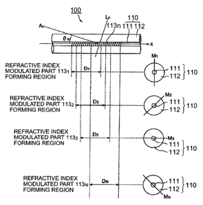
Fig. 2 is an explanatory view of the optical wave guide
type diffraction grating device (tilt type diffraction
grating device) 1 in accordance with an embodiment. This
drawing shows a sectional view cut along a plane including
the optical axis, and sectional views cut along planes
perpendicular to the opticalaxis. The tilt type diffraction
grating device 1 in accordance with this embodiment shown
in the drawing is one in which N (N being an integer not
smaller than 2 ) refractive index modulated parts 131 to 13N
are formed along the longitudinal direction of an optical
fiber 10 which is an optical wave guide. The optical fiber
10 is based on silica glass, and includes a core region 11
doped with Ge02, and a cladding region 12 surrounding the
core region 11.
For each refractive index modulated part 13" (n being
a given integer of at least 1 but not greater than N), Ln
is a refractive index level plane yielding the same refractive
index, A" is a line, perpendicular to the refractive index
level plane Ln, intersecting the optical axis (x axis) of
12
CA 02453533 2004-O1-09
FPOl-0235-00
the optical fiber 10, A" is the angle formed between the line
A" and the optical axis, and M" is the deflection angle plane
formed by the line An and the optical axis.
In each refractive index modulated part 13", the line
An is not parallel to the optical axis, whereas the angle
9n formed between the line An and the optical axis is not
zero. Namely, each refractive index modulated part 13" is
one in which a refractive index modulation having a period
I~n is formed in the core region 11 along the line A" inclined
by the angle 6" with respect to the optical axis. The
respective deflection angle planes M~ of refractive index
modulated parts 13" do not coincide with each other. Namely,
in given two refractive index modulated parts 131, 13"2 of
the N refractive index modulated parts 131 to 13N, their
respective deflection angle planes Mnl, M"2 do not coincide
with each other.
In the N refractive index modulated parts 131 to 13N,
two refractive index modulated parts 13"1, 13"2 have forming
areas overlapping each other at least partially. In the
drawing, for example, the forming area of the refractive
index modulated part 131 partially overlaps the forming area
of the refractive index modulated part 132, the forming area
of the refractive index modulated part 133, and the forming
area of the refractive index modulated part 13N. Preferably,
all the respective forming areas of the N refractive index
modulated parts 131 to 13N coincide with each other.
13
CA 02453533 2004-O1-09
FPO1-0235-00
Thus, the tilt type diffraction grating device 1 in
accordance with this embodiment is formed with N refractive
index modulated parts 131 to 13N, the angle 6n of each refractive
index modulated part 13" is not zero, the respective
deflection angle planesM~ofrefractiveindexmodulatedparts
13n do not coincide with each other, and given two refractive
index modulated parts 13n1, 13n2 have respective forming areas
overlapping each other at least partially. Thus configured
tilt type diffraction grating device 1 is a short one whose
polarization-dependent loss is reduced.
Preferably, the respective deflection angle planes Ml
to MN of the N refractive index modulated parts 131 to 13N
shift from each other at intervals of 180 degrees/N about
the optical axis of the optical fiber 10. When N = 2, for
example, the deflection angle planes Ml and M2 are orthogonal
to each other. When N = 3, for example, the deflection angle
planes Ml to M3 shift from each other at intervals of 60 degrees
about the optical axis of the optical fiber 10. When the
deflection angle planes M1 to MN are arranged as such, the
polarization-dependent loss is efficiently reduced in the
tilt type diffraction grating device 1.
Preferably, in the N refractive index modulated parts
131 to 13N, lines A,., form the same angle 8" with the optical
axis, respective forming areas have the same length Dn along
the longitudinal direction of the optical fiber 10,
respectiverefractiveindex modulation periodsare thesame,
14
CA 02453533 2004-O1-09
FPOl-0235-00
and respective refractive index modulation amplitudes are
the same. When each refractive index modulated part 13n is
formed as such, the polarization-dependent loss is
efficiently reduced in the tilt type diffraction grating
device 1.
Preferably, at a wavelength yielding the maximum
transmission loss, the polarization-dependent loss of the
tilt type diffraction grating device 1 in accordance with
this embodiment is not greater than 1/10 of the transmission
loss maximum value. Such a tilt type diffraction grating
device is favorably used as an optical apparatus (or a part
thereof) which is required to have a low
polarization-dependent loss in the field of optical
communications, and can favorably be used as a gain equalizer
for equalizing the gain of an optical fiber amplifier, for
example.
A method of making the optical waveguide type
diffraction grating device (tilt type diffraction grating
device) 1 in accordance with this embodiment will now be
explained. Figs. 3 and 4A - 4D are drawings for explaining
the method of making an optical waveguide type diffraction
grating device in accordance with this embodiment. Fig. 3
shows a perspective view, whereas Figs . 4A- 4D shows sectional
views cut along a plane perpendicular to the optical axis .
First, an optical fiber 10, a phase grating mask 20,
and a light source 30 are prepared. As mentioned above, the
CA 02453533 2004-O1-09
FP01-0235-00
optical fiber 10 is based on silica glass, and includes a
core region 11 doped with Ge02 and a cladding region 12
surrounding the core region 11. The phase grating mask 20
is one in which one surface of a flat silica glass sheet
is formed with a phase grating made of groove-like protrusions
and recesses having a period of 211. The light source 30 is
one outputting light having a wavelength which induces a
refractive index change in the core region 11 of the optical
fiber 10 (hereinafter referred to as "refractive index change
inducing light"). For example, a KrF excimer laser light
source outputting a laser beam having a wavelength of 248
nm as refractive index change inducing light is used.
Then, as shown in Fig. 3, the phase grating mask 20
is arranged laterally with respect to the optical fiber 10
such that its surface formed with the phase grating opposes
the optical fiber 10. At that time, the direction of grooves
in the phase grating mask 20 inclines by an angle A1 with
respect to a plane perpendicular to the optical axis of the
optical fiber 10. In the state where they are arranged as
such, refractive index change inducing light UV outputted
from the light source 30 perpendicularly irradiates the phase
grating mask 20. Upon irradiation with the refractive index
change inducing light UV, (+)first-order diffraction light
and (-)first-order diffraction light occur due to a
diffracting action of the phase grating mask 20, and interfere
with each other, thereby generating interference fringes
16
CA 02453533 2004-O1-09
FPO1-0235-00
with a period h. In the core region 11 doped with Ge02 in
the optical fiber 10, the refractive index rises in response
to the magnitude of energy of the refractive index change
inducing light at each position of the interference fringes,
thereby forming a refractive index modulated part 131. In
this refractive index modulated part 131, letting A1 be a
line, perpendicular to a refractive index level plane L1,
intersecting the optical axis of the optical fiber 10, the
angle formed between the line A1 and the optical axis is 81,
whereas the deflection angle plane Ml formed by the line Al
and the optical axis is parallel to the plane of the phase
grating mask 20 (see Figs. 3 and 4A).
Irradiation with the refractiveindex change inducing
light UV for a predetermined period of time in the state
of arrangement shown in Fig. 4A as such forms the first
refractive index modulated part 131. After the formation,
the irradiation with refractive index change inducing light
UV is interrupted, while the optical fiber 10 is rotated
by a predetermined angle about the optical axis during this
interruption, so as to attain the state of arrangement shown
in Fig. 4B. Then, irradiation with the refractive index
change inducing light W for a predetermined period of time
in the state of arrangement shown in Fig. 4B forms the second
refractive index modulated part 13z. In thus formed second
refractive index modulated part 132, letting A2 be a line,
perpendicular to a refractive index level plane LZ,
17
CA 02453533 2004-O1-09
FPO1-0235-00
intersecting the optical axis of the optical fiber 10, the
angle formed between the line A2 and the optical axis is 82,
whereas the deflection angle plane M2 formed by the line AZ
and the optical axis is parallel to the plane of the phase
grating mask 20. The deflection angle plane M2 of the second
refractive index modulated part 132 does not coincide with
the deflection angle plane M1 of the already formed first
refractive index modulated part 131.
After the second refractive index modulated part 132
is formed, the irradiation with refractive index change
inducing light UV is interrupted, while the optical fiber
10 is rotated by a predetermined angle about the optical
axis during this interruption, so as to attain the state
of arrangement shown in Fig. 4C. Then, irradiation with the
refractiveindex changeinducinglight W for a predetermined
period of time in the state of arrangement shown in Fig.
9C forms the third refractive index modulated part 133. In
thus formed third refractive index modulatedpart 133, letting
A3 be a line, perpendicular to a refractive index level plane
L3, intersecting the optical axis of the optical fiber 10,
the angle formed between the line A3 and the optical axis
is 03, whereas the deflection angle plane M3 formed by the
line A3 and the optical axis is parallel to the plane of the
phase grating mask 20. The deflection angle plane M3 of the
third refractive index modulated part 133 does not coincide
with any of the deflection angle plane Ml of the already formed
18
CA 02453533 2004-O1-09
FPOl-0235-00
first refractive index modulated part 131 and the deflection
angle plane M2 of the already formed second refractive index
modulated part 132.
In a similar manner, the fourth to N-th refractive index
modulated parts 139 to 13N are formed successively. When
forming the N-th refractive index modulated part 13N,
irradiation with the refractive index change inducing light
UV for a predetermined period of time in the state of
arrangement shown in Fig. 4D forms the N-th refractive index
modulated part 13N. In thus formed N-th refractive index
modulated part 13N, letting AN be a line, perpendicular to
a refractive index level plane LN, intersecting the optical
axis of the optical fiber 10, the angle formed between the
line AN and the optical axis is 8N, whereas the deflection
angle plane MN formed by the line AN and the optical axis
is parallel to the plane of the phase grating mask 20. The
deflection angle plane MH of the N-th refractive index
modulated part 13N does not coincide with any of the deflection
angle planes Ml to MN_1 of the already formed first to (N-1 ) -th
refractive index modulated parts 131 to 13N_1.
Though individual values of 6n are the same when the
position of the phase grating mask 20 is held at a fixed
position, the values of 8n can be made different from each
other if the phase grating mask 20 is rotated on a plane
thereof . Also, though all the refractive index modulation
periods along respective lines An in the refractive index
19
CA 02453533 2004-O1-09
FPO1-0235-00
modulated parts 13,., have the same value when a single phase
grating mask 20 is used, the refractive index modulation
periods along respective lines A~ in the refractive index
modulated parts 13n can be made different from each other
if the phase grating mask is replaced with one having a
different phase grating period.
Thus, in the method of making an optical waveguide type
di f fraction grating device in accordance with this embodiment,
N refractive index modulated parts 131 to 13N are successively
formed along a longitudinal direction of the optical fiber
10 such that the line A" perpendicular to the refractive index
level plane Ln is not parallel to the optical axis of the
optical fiber 10 (i.e., A~ ~ 0) . Also, the n-th refractive
index modulated part 13" is formed such that its deflection
angle plane M~ does not coincide with any of the respective
deflection angle planes Ml to M~_1 of the already formed first
to (n-1)-th refractive index modulated parts 131 to 13n_i.
Further, given two of the N refractive index modulated parts
131 to 13N are formed such that their respective forming areas
overlap each other at least partially. Thus, the tilt type
diffraction grating device 1 in accordance with this
embodiment is made.
In particular, it is preferred that the optical fiber
10 be rotated about the optical axis by a predetermined angle
of 180 degrees/N after the (n-1)-th refractive index
modulated part 13n_1 is formed, and then the n-th refractive
CA 02453533 2004-O1-09
FPO1-0235-00
index modulated part 13n be formed. In thus made tilt type
diffraction grating devicel,therespective deflection angle
planes M1 to MN of the N refractive index modulated parts
131 to 13N shift from each other at intervals of 180 degrees/N
about the optical axis of the optical fiber 10, whereby the
polarization-dependent loss is efficiently reduced.
Preferably, the individualrefractiveindex modulated
parts 13n are formed such that lines An perpendicular to
respective refractive index level planes Ln form the same
angle A~ with the optical axis of the optical fiber 10,
respective forming areas have the same length Dn along the
longitudinal direction of the optical fiber 10, respective
refractive index modulation periods are the same, and
respective refractive index modulation amplitudes are the
same. Thus made tilt type diffraction grating device 1
becomesone whose polarization-dependentlossisefficiently
reduced.
Preferably, when forming each refractive index
modulated part 13", the transmission loss or
polarization-dependent loss of the tilt type diffraction
grating device 1 in the process of making is monitored. Thus
made tilt type diffraction grating device 1 becomes one whose
polarization-dependent loss is efficiently reduced.
An example of the optical waveguide type diffraction
grating device (tilt type diffraction grating device) 1 in
accordance with this embodiment and method of making the
21
CA 02453533 2004-O1-09
FPOl-0235-00
same will now be explained. In this example, the optical
fiber 10 was one in which not only the core region 11 but
also the cladding region 12 was doped with Ge02. The period
of the phase grating mask 20 was not fixed but gradually
changed along a direction perpendicular to the direction
of grooves, with a center period of 1.0650 dun and a period
changing rate of 10.0 nm/cm. Employed as the light source
30 was a KrF excimer laser light source outputting a laser
beam having a wavelength of 248 nm as refractive index change
inducing light.
Thus made tilt type diffraction grating device 1 of
this example had two refractive index modulated parts 131,
132. The two refractive index modulated parts 131, 132 each
had a forming area with a length of 5 mm and totally overlapped
each other. The deflection angle plane Ml of the refractive
index modulated part 131 and the deflection angle plane MZ
of the refractive index modulated part 132 were orthogonal
to each other.
In the manufacturing method of this example, the first
refractive index modulated part 131 was initially formed,
the optical fiber 10 was rotated by 90 degrees about the
opticalaxis thereafter while theirradiation with refractive
index change inducing light W was interrupted, and then
the second refractive index modulated part 132 was formed.
When forming each of the two refractive index modulated parts
131, 132, the transmission loss of the tilt type diffraction
22
CA 02453533 2004-O1-09
FPOl-0235-00
grating device 1 in the process of making was monitored.
In this example, the target value of transmission loss
at a wavelength yielding the maximum transmission loss was
set to 1 dB. When forming the first refractive index
modulated part 131, the irradiation with refractive index
change inducing light UV was interrupted at the time when
the monitored transmission loss became 1/2 (0.5 dB) of the
target value. Subsequently, when forming the second
refractive index modulated part 132, the irradiation with
refractive index change inducing light UV was interrupted
at the time when the monitored transmission loss became the
target value (1 dB) . Fig. 5Ais a graph showing a transmission
characteristic at the time when the first refractive index
modulated part 131 was completely formed, whereas Fig. 5B
is a graph showing a transmission characteristic at the .time
when.the second refractive index modulated part 132 was
completely formed. As shown in this graph, the maximum value
of transmission loss in the tilt type diffraction grating
device 1 in accordance with this example was 0.5 dB at the
time when the first refractive index modulated part 131 was
completely formed, and 1.0 dB at the time when the second
refractive index modulated part 132 was completely formed.
Fig. 6Ais a graph showing a transmission characteristic
of the tilt type diffraction grating device in accordance
with this example, whereas Fig. 6B is a graph showing a
polarization-dependent loss characteristic of thetilt type
23
CA 02453533 2004-O1-09
FPO1-0235-00
diffraction grating device in accordance with this example.
Fig. 7A is a graph showing a transmission characteristic
of the tilt type diffraction grating device in accordance
with a comparative example, whereas Fig. 7B is a graph showing
a polarization-dependent loss characteristic of the tilt
type diffraction grating device in accordance with the
comparative example. Here, the tilt type diffraction
grating device in accordance with the comparative example
has only one refractive index modulated part without
overwriting.
As can be seen when Figs . 6A and 7A are compared with
each other, the respective transmission spectra of the tilt
type diffraction grating devices in accordance with the
example and comparative example had forms similar to each
other, each yielding the maximum transmission loss value
of about 0.6 dB. However, as can be seen when Figs. 6B and
7B are compared with each other, the maximum
polarization-dependent loss value of the tilt type
diffraction grating devicein accordance withthe comparative
example was about 0.125 dB, whereas the maximum
polarization-dependent loss value of the tilt type
diffraction grating device in accordance with the example
was about 0.03 dB. The maximum polarization-dependent loss
value of the tilt type diffraction grating device in
accordance with the example was about 1/4 of the maximum
polarization-dependent loss value of the tilt type
24
CA 02453533 2004-O1-09
FPO1-0235-00
diffraction grating devicein accordance with the comparative
example, and about 1/20 of the maximum transmission loss
value of the tilt type diffraction grating device in
accordance with the example.
Fig. 8 is an explanatory view of an optical waveguide
type diffraction grating device (tilt type diffraction
grating device) 2 according to another embodiment. This
drawing illustrates a sectional view cut along a plane
including the optical axis, and a sectional view cut along
a plane perpendicular to the optical axis. The tilt type
diffraction grating device200according to thisembodiment,
which is illustrated in this drawing, has N (where N is an
integer of 2 or above) refractive index modulated parts 2301
- 23N formed along the longitudinal direction of the optical
fiber 20, which is the optical waveguide. The optical fiber
has silica glass as its base, and comprises a Ge02-doped
core region 21, and a cladding region 220 surrounding this
core region 21.
For each refractive index modulated part 23~ (where
20 n is an arbitrary integer not less than 1 and not greater
than N), the refractive index level plane, wherein the
refractive index becomes level, is expressed by Ln; the line
perpendicular to the refractive index level plane Ln,
intersecting the optical axis (x axis) of the optical fiber
20, is expressed by A~; the angle formed between the line
An and the optical axis is expressed by 6n; and the deflection
CA 02453533 2004-O1-09
FPO1-0235-00
angle plane formed by the line A" and the optical axis is
expressed by M". The areas of formation, refractive index
level plane Ln, line An, and angle 6n of the refractive index
modulated parts 23n are all as previously explained.
This tilt type diffraction grating device 2 is
characterized in that the deflection angle planes Mn of the
refractive index modulated parts 23" shift from each other
at intervals of 360 degrees/N about the optical axis . Note
that, in the drawing, N = 4. In this case, the double
refraction characteristic which is caused by nonaxisymmetry
in each of the refractive index modulated parts 231 and 233,
the deflection angle planes M~ of which differ from each other
by 180°, is offset, and since the double refraction
characteristic which is caused by nonaxisymmetry in each
of the refractive index modulated parts 2303 and 23q, the
deflection angle planes Mn of which differ from each other
by 180°, is offset, the polarization-dependent loss in the
optical waveguide type diffraction grating device 2 is
reduced efficiently. Note that here, nonaxisymmetry
indicates that the rise in the refractive index is increasing
on the incident side of the refractive index change-inducing
light in the refractive index modulated part 231, which is
formed byirradiating refractiveindex change-inducinglight
onto the optical fiber 20. Consequently, by forming the
refractive index modulated parts 2301 and 233 by irradiating
refractiveindex change-inducinglight onto the opticalfiber
26
CA 02453533 2004-O1-09
FPO1-0235-00
20 from opposite directions, the double refraction
characteristic caused by the nonaxisymmetry [in these
refractive index modulated parts] is offset.
In this tilt type diffraction grating device 2 also,
it is suitable for the polarization-dependent loss to be
1/10 or less of the largest transmission loss value in the
wavelength at whichtransmissionlossisgreatest. Thiskind
of tilt type diffraction grating device 2 may also be used
appropriately as an optical device (or one part thereof)
in which low polarization-dependent loss is required, in
the field of optical transmission, and for example, may be
used appropriately as a gain equalizer for equalizing the
gain in an optical fiber amplifier.
Figs . 9A to 11B are each graphs showing the wavelength
dependence of the transmittance T and
polarization-dependencelossPDL respectivelyin three types
of tilt type diffraction grating devices. Figs. 9A and 9B
are graphs showing characteristics of a tilt type diffraction
grating device 1 in which refractive index change inducing
light is irradiated from only one direction to form one
refractive index modulated part . Figs . 9A and 9B are graphs
showing characteristics of a tilt type diffraction grating
device 2 in which refractive index change inducing light
is irradiated from two directions which differ from each
other by 90° to form two refractive index modulated parts .
Figs. 11A and 11B are graphs showing characteristics of a
27
CA 02453533 2004-O1-09
FPO1-0235-00
tilt type diffraction grating device 2 in which refractive
index change inducing light is irradiated from four
directions, differing from each other by 90° at a time, to
form four refractive index modulated parts.
; In each of;the tilt type diffraction grating device 1 and
i
the tilt type diffraction grating device 2, the refractive
index modulated parts are formed so as to overlap each other .
As can be understood by comparing Figs. 9A, 10A and
11A, the wavelength dependence of the transmittance T in
each of the three types of tilt type diffraction grating
device is substantially the same. On the other hand, as can
be understood by comparing Figs. 9B, lOB and 11B, the
polarization-dependencelossPDL ofthe tilt type diffraction
grating device formed with one refractive index modulated
part reaches 0.127dB, whereas the polarization-dependence
loss PDL of the tilt type diffraction grating device 1 is
as small as 0.023dB, and the polarization-dependence loss
PDL of the tilt type diffraction grating device 2 is, at
0.016d8, even smaller.
Industrial Applicability
According to the present invention, as explained in
detail in the foregoing, N (N being an integer not smaller
than 2) refractive index modulated parts are formed,
respective lines perpendicular to refractive index level
planes of the refractive index modulated parts are not
parallel to the optical axis of the optical waveguide,
28
CA 02453533 2004-O1-09
FPOl-0235-00
respective deflection angle planes of refractive index
modulated parts do not coincide with each other, and given
two refractiveindex modulated partshave respective forming
areas overlapping each other at least partially. Thus
configured opticalwaveguide type diffraction grating device
becomes a short one whose polarization-dependent loss is
reduced.
29