Note: Descriptions are shown in the official language in which they were submitted.
CA 02453601 2004-01-12
WO 03/010550 PCT/US02/17532
INTEGRATED TESTING OF SERIALIZER/DESERIALIZER IN FPGA
FIELD OF THE INVENTION
The present invention relates generally to field
programmable gate arrays (FPGAs) and in particular the
present invention relates to integrated testing of FPGAs.
BACKGROUND OF THE INVENTION
The development of optical fiber transmission of
digital data streams has given rise to a data transfer
protocol and interface system termed Fiber-Channel. Fiber-
Channel technology involves coupling various computer
systems together with optical fiber or a fiber-channel-
compatible electrically conductive (copper) cable and
allows extremely rapid data transmission speeds between
machines separated by relatively great distances. A Fiber
Channel family of standards (developed by the American
National Standards Institute (ANSI)) defines a high speed
communications interface for the transfer of large amounts
of data between a variety of hardware systems such as
personal computers, workstations, mainframes,
supercomputers, storage devices and servers that have Fiber
Channel interfaces. Use of Fiber Channel is proliferating
in client/server applications that demand high bandwidth
and low latency I/O. Fiber Channel achieves high
performance, which is critical in opening the bandwidth
limitations of current computer-to-storage and computer-to-
computer interfaces at speeds up to 1 gigabit per second or
faster.
Information to be transmitted over a fiber wire or
cable is encoded, 8 bits at a time, into a 10-bit
Transmission Character that is subsequently serially
transmitted bit by bit. Data provided over a typical
computer system's parallel architecture is encoded and
framed such that each data byte (8-bits from the point of
view of the computer system) is formed into a Transmission
Character in accordance with the Fiber-Channel 8B/10B
transmission code. The resulting 8B/10B character is then
1
CA 02453601 2004-01-12
WO 03/010550 PCT/US02/17532
transmitted as 10 sequential bits at a 1.06 GHz data rate.
Likewise, an incoming 8B/10B encoded transmission character
must be serially received at a 1.06 GHz data rate and
converted (framed) into the corresponding 10-bit
transmission character. The 10-bit transmission character
is then further decoded into an 8-bit byte recognizable by
conventional computer architectures.
In data processing systems and data networks
information is transferred over serial and parallel buses
between systems, and an interface exists to provide
compatibility between the data processing system and the
bus to which it connects. Moreover some networks provide
an interface between diverse buses with different
characteristics. As an example, an interface may couple a
data processing system PCI bus to a fiber channel. The PCI
bus operates with parallel data paths whereas a fiber
channel operates with serial data paths.
A serializer/deserializer (SERDES) forms an integral
part of a fiber channel interface circuit between the
serialized data paths of the fiber channel and the parallel
data paths of an integrated circuit interface. A fiber
channel interface connects to the SERDES through a
connection and to a frame processing circuit through
parallel data buses that essentially transfer information
to and from the frame processing circuit.
As integrated circuits continue to increase in
complexity, it is increasingly difficult to test the
device. In particular, in order to test an integrated
circuit, a large number of test patterns and configurations
may be required. The response to the test patterns is then
monitored to determine if defects.are present. This
testing is time-consuming and may use all of the
input/output pins of the integrated circuit. Accordingly,
it is known to provide a circuit(s) in the integrated
circuit device itself to provide a Built-In Self Test
(BIST).
Programmable logic devices (PLDs) are a well-known
type of digital integrated circuit that may be programmed
by a user (e.g., a circuit designer) to perform specified
2
CA 02453601 2004-01-12
WO 03/010550 PCT/US02/17532
logic functions. One type of PLD, the field-programmable
gate array (FPGA), typically includes an array of
configurable logic blocks, or CLBS, that are programmably
interconnected to each other and to programmable
input/output blocks (IOBs). FPGAs can be provided that
includes a high speed interconnect that require a SERDES.
For the reasons stated above, and for other reasons
stated below which~will become apparent to those skilled in
the art upon reading and understanding the present
specification, there is a need in the art for a method of
testing high speed SERDES circuitry in an FPGA.
SUMMARY OF THE INVENTION
The above-mentioned problems with testing high speed
SERDES circuitry in an FPGA and other problems are
addressed by the present invention and will be understood
by reading and studying the following specification.
In one embodiment, a field programmable gate array (FPGA)
comprises a logic array, a data communication connection,
and a serializer/deserializer circuit coupled to the data
communication connection and the logic array. The logic
array is programmable to perform test operations on the
serializer/deserializer circuit. After testing is
completed, the programmable circuitry may be re-programmed
to perform the end user application, thereby creating zero
added cost for providing the test feature in the silicon.
in another embodiment, a field programmable gate
array (FPGA) comprises input and output data communication
connections, a serializer/deserializer circuit coupled to
the input and output data communication connections, and a
logic array programmed to generate a test data pattern
coupled to the output data connection. The logic array is
further programmed to check a data pattern received on the
input connection while performing a built in self test
operation. After test, the,circuit may be re-programmed as
stated above.
A method of testing a high speed interconnect
circuit of a field programmable gate array (FPGA) comprises
generating a test pattern using programmed logic circuitry
3
CA 02453601 2006-10-03
74842-38
of the FPGA, outputting the test pattern on an output
connection, coupling the test pattern to an input connection
of the high speed interconnect circuit, evaluating data
received on the input connection using the programmed logic
circuitry, and storing data indicating a result of the
evaluation. After test, the circuit may be re-programmed as
stated above.
According to another aspect the invention provides
a test system comprising: a test circuit; and a field
programmable gate array (FPGA) coupled to the test circuit,
wherein the FPGA comprises, input and output data
communication connections coupled together through the test
circuit, a serializer/deserializer (SERDES) circuit coupled
to the input and output data communication connections, and
a logic array programmed to generate a test data pattern
coupled to the output data communication connection, the
logic array is further programmed to check a data pattern
received on the input connection while performing a built in
self test operation.
According to another aspect the invention provides
a method of testing a serializer/deserializer (SERDES)
circuit of a field programmable gate array (FPGA)
comprising: programming a logic array of the FPGA;
generating a test pattern using the programmed logic array
of the FPGA; outputting the test pattern on an output
connection of the SERDES circuit; externally coupling the
test pattern to an input connection of the SERDES circuit;
using the programmed logic array, evaluating data received
on the input connection; storing data indicating a result of
the evaluation in a memory circuit of the FPGA; and re-
programming the logic array to perform an end user
application.
4
CA 02453601 2006-10-03
74842-38
BRIEF DESCRIPTION OF THE DRAWINGS
Figure 1 illustrates a logic array of a prior art
field programmable gate array (FPGA);
Figure 2 is a block diagram of an embodiment of an
FPGA of the present invention;
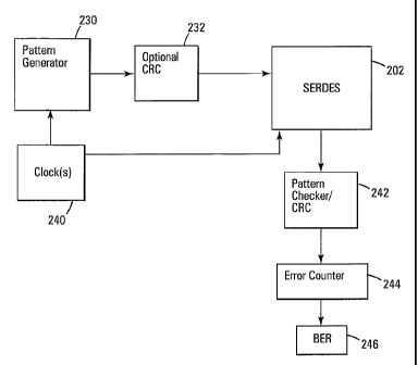
Figure 3 is a block diagram of an FPGA test
circuit of an embodiment of the present invention; and
Figure 4 illustrates an FPGA coupled to a tester
circuit.
DETAILED DESCRIPTION OF THE DRAWINGS
In the following detailed description of the
preferred embodiments, reference is made to the accompanying
drawings, which form a part hereof, and in which is shown by
way of illustration specific preferred embodiments in which
the inventions may be practiced. These embodiments are
described in sufficient detail to enable those skilled in
the art to practice the invention, and it is to be
understood that other embodiments may be utilized and that
logical, mechanical and electrical changes may be made
without departing from the spirit and scope of the present
invention. The following detailed description is,
therefore, not to be taken in a limiting sense, and the
scope of the present invention is defined only by the
claims.
Figure 1 is a simplified block diagram of a prior
art field-programmable gate array (FPGA) 100. FPGA 100
includes an array of configurable logic blocks (CLBs) 110
5
CA 02453601 2006-10-03
74842-38
that are programmably interconnected to each other and to
programmable input/output blocks (IOB's) 120. The
interconnections are provided by a complex interconnect
matrix represented as horizontal and vertical interconnect
lines 130 and 140. Detailed descriptions of FPGA
architectures may be found in U.S. Patents 34,363 and
5,914,616.
This collection of configurable elements and
interconnect may be customized by loading configuration data
into internal configuration memory cells (not shown) that
define how the CLBs, interconnect lines, and IOBs are
configured. A detailed description of an FPGA configuration
structure may be found in U.S. Patent 5,844,829. The
configuration data may be read from memory or written into
FPGA 100 from an external device. The collective program
states of the individual memory cells then determine the
function of FPGA 100. A value of FPGA 100 is that its
logical function can be changed at will by loading new or
partially new or different configurations (re-programming).
Such changes are accomplished by loading the configuration
memory cells and resetting (or presetting) the user logic,
or through the configurable logic itself (self re-
configuration).
CLBs 110 and IOBs 120 additionally include user-
accessible memory elements (not shown), the contents of
which can be modified as FPGA 100 operates as a logic
circuit. These user-accessible memory elements, or "user
logic", include block RAM, latches, and flip-flops. The
data stored in user logic is alternatively referred to as
5a
CA 02453601 2004-01-12
WO 03/010550 PCT/US02/17532
"user data" or "state data."
The present invention provides an FPGA that has a bi-
directional interface for high-speed communication, such as
gigabit communications. A serializer/deserializer (SERDES)
is provided to interface with the external high-speed bus.
During fabrication, it is desired to test the SERDES
circuit for both functional integrity and proper operation
at communications speeds such as 3+ gigabits per second.
As explained below, embodiments of the present invention'
allow testing of the SERDES circuit at communication speeds
and while stressed.
One embodiment of the present FPGA includes sixteen
SERDES circuits that are each capable of communicating at
gigabit speeds. The SERDES circuits are coupleable to
internal digital clock manager (DCM) circuits. The DCMs
generate both a transmit clock and a receive clock for the
SERDES circuits. The DCMs are capable of adding noise or
jitter to the clock signals. In addition, the DCMs can
create frequency offsets and shift phase by predetermined
amounts. As such, the FPGA can add stress to the SERDES
circuit by manipulating the clock signal characteristics.
The FPGA logic components can be programmed during
testing to operate as test circuitry to perform operation
tests of the SERDES circuits. This built-in-self-test
(BIST) feature provides an advantage not available in
conventional integrated circuits. Test circuitry required
to implement a BIST for testing high-speed SERDES circuits
would be too extensive and cost prohibitive to fabricate as
part of an integrated circuit.
To test the SERDES circuitry, the FPGA logic is
programmed to provide a pseudo random bitstream generator,
stress pattern generators, cyclical redundancy check (CRC)
circuitry and bit error rate testers. As explained below,
the pseudo random bitstream generator can be implemented
using a linear feedback shift register (LFSR).
Referring to Figure 2, a block diagram of an FPGA
200 the present invention is described. The device
includes a SERDES circuit 202 coupled with external
transmit 204 and receive 206 connections. The SERDES
6
CA 02453601 2004-01-12
WO 03/010550 PCT/US02/17532
circuit is coupled to the internal logic circuit of the
FPGA. Digital clock manager circuits 212 are coupled to
the logic circuits to provide transmit and receive clock
signals. By coupling the outputs of the SERDES circuit to
its inputs, the logic applies test patterns to the
communication circuitry. For stress, jitter can be added
to the clock signals while the test is performed. The
results of the test are then stored in the FPGA internal
memory 214. The test results can be subsequently read to
determine if the device encountered performance problems.
Figure 3 illustrates a block diagram of a bit error
rate tester of the present invention. The tester includes
a pattern generator 230 programmed into the FPGA array.
The pattern generator can be implemented as a linear
feedback shift register. An optional cyclical redundancy
check (CRC) circuit 232 can be programmed in the FPGA to
provide CRC characters to the test program. Other error
checking characters can be used, including simple parity
checks. As such, the present invention is not limited to
CRC characters. The test data pattern is coupled to the
SERDES channel 202 under test. The clock(s) 240 used to
control the test pattern can be stressed, as indicated
ab'ove, to enhance the testing operation. The data received
by the SERDES is then checked for possible errors using
check circuitry 242 programmed in the FPGA array. If CRC
232 is provided, the received CRC characters are also
checked. An error counter 244 is programmed in the FPGA
logic to maintain a total count of errors encountered
during testing. The number of errors from the counter is
analyzed by bit error rate (BER) circuit 246 to determine
the number of errors encountered per the number of bits
tested to provide a BER. The BER can be stored in memory
for retrieval or a pass-fail code can be stored based upon
a threshold BER. That is, a tester can read the FPGA
memory to determine if the part passed the test, or it can
analyze a stored BER to determine if the device meets
acceptable criteria.
A test system is illustrated in Figure 4 that
includes a test circuit 300 and an FPGA 200. The FPGA has
7
CA 02453601 2006-10-03
74842-38
been programmed as described above to provide a built in
self-test (BIST) of data communication circuitry provided in
the FPGA. The test circuitry can be a microprocessor device
or a test specific device such as the ring oscillator
described in U.S. Patent 6,232,845. If a microprocessor is
used, it may also be implemented as a dedicated core of
logic within the FPGA, or as a set of programmed logic
blocks performing the same microprocessor function in the
CLBs. During a test operation, the FPGA generates a test
pattern that is output on the output communication
connection. The output connection is coupled to the
FPGA input connection and the received data pattern is
evaluated. If errors are detected, data indicating a status
of the FPGA error rate is programmed into a memory of the
FPGA. The test circuit can access, or read, the contents of
the FPGA memory to determine if the FPGA is good, or has an
acceptable error rate level. The FPGA of the present
invention has an advantage over fabricating test specific
circuitry in an integrated circuit to perform a BIST of a
high-speed communication circuit. Specifically, the FPGA of
the present invention includes a digital clock manager
circuit that can generate clock signals to stress the test
operation by varying the frequency, phase and jitter
magnitude and jitter frequencies of the clock signals.
Implementing test specific circuitry in an integrated
circuit to perform these tests would be space and cost
prohibitive. The programmable logic can be re-used for the
end application by re-programming, resulting in zero cost
for the test feature.
8
CA 02453601 2006-10-03
74842-38
Conclusion
A field programmable gate array (FPGA) device has
been described that includes a high-speed
serializer/deserializer (SERDES). The field programmable
gate array allows built in testing of the SERDES at
operating speeds. A digital clock manager circuit allows
clock signals coupled to the SERDES to be modified during
the test operations to stress the SERDES circuit. The
8a
CA 02453601 2004-01-12
WO 03/010550 PCT/US02/17532
logic array of the FPGA can be programmed to generate a
test pattern and to analyze data received by the SERDES
circuit. Cyclic redundancy check (CRC) characters can also
be generated using the logic array. During testing, the
FPGA can perform extensive tests on the communication
circuitry and store the results of the testing. An
external tester can read the results of the test without
substantial test time or complicated test equipment.
Although specific embodiments have been illustrated
and described herein, it will be appreciated by those of
ordinary skill in the art that any arrangement, which is
calculated to achieve the same purpose, may be substituted
for the specific embodiment shown. This application is
intended to cover any adaptations or variations of the
present invention. Therefore, it is manifestly intended
that this invention be limited only by the claims and the
equivalents thereof.
9