Note: Descriptions are shown in the official language in which they were submitted.
CA 02453783 2004-O1-14
DESCRIPTION
OPTICAL WAVEGUIDE MODULE
Technical Field
The present invention relates to an optical
waveguide module having optical waveguides provided
on its substrate.
Background Art
For some optical circuits using optical
waveguides such as optical fibers or planar optical
waveguides, it may be desirable to keep constant the
light intensity of signal light transmitted in each
optical waveguide, or otherwise adjust the light
intensity of the signal light to a suitable value.
In such a case, the light intensity of the signal
light is monitored in the optical circuit, or
additionally the monitored result is used as a basis
for controlling the light intensity.
Disclosure of Invention
For monitoring the light intensity of the
signal light as described above, a method is
conventionally used in which an optical coupler is
provided along the optical waveguide to split part
of the signal light. In this method, an optical
coupler is provided at a predetermined position
along the optical waveguide to split about a few
percent of the signal light. The light intensity of
1
CA 02453783 2004-O1-14
the split light is monitored by a photodetector, and
thereby the light intensity of the signal light
transmitted in the optical waveguide is monitored.
Here, when an optical coupler is used as just
described, the number of optical components
constituting the optical circuit increases, and
further they needs to be fusion spliced. This
causes a problem of making the configuration and
manufacturing process of the optical circuit more
complex.
On the contrary, another method of monitoring
light intensity has been proposed, which draws part
of signal light by reflection without using optical
couplers. One such device is described in, for
example, Kasahara et al., "PLC hybrid integrated-
type 8ch tapped optical power monitor", the 2002
General Conference of the Institute of Electronics,
Information and Communication Engineers, C-3-49.
In this device, the signal light is propagated
in a planar-waveguide-type optical waveguide. A
multilayer film filter is inserted inside a groove
formed in the planar-waveguide-type optical circuit
to reflect part of the signal light. The signal
light reflected by the multilayer film filter is
then detected by a photodiode, and thereby the light
intensity of the signal light is monitored. Also in
2
CA 02453783 2004-O1-14
this monitoring device, shading grooves filled with
light absorbing material are formed between the
multilayer film filter and the photodiode or in
other predetermined regions in order to inhibit
crosstalk between channels due to stray light.
However, in such a configuration where the
propagated signal light is monitored by means of
reflected light from the reflection filter, there is
a problem that inside the groove for inserting the
reflection filter in the optical waveguide, extra
scattered light is generated by reflection of light
or otherwise at various regions. Such scattered
light may cause degradation of monitoring
characteristics for the signal light, such as the
S/N ratio at the photodiode for detecting the
reflected light from the reflection filter and the
crosstalk between adjacent photodiodes.
The present invention is directed to solving
the above problems. An object of the present
invention is to provide an optical waveguide module
capable of reducing the influence of extra scattered
light, and enhancing the monitoring characteristics
for the signal light.
To achieve such an object, an optical waveguide
module according to the present invention comprises:
(1) an optical circuit configured to include a
3
CA 02453783 2004-O1-14
substrate and an optical waveguide provided on the
substrate, and having a groove formed to traverse a
predetermined position of the optical waveguide; (2)
a reflection filter, placed inside the groove of the
optical circuit to span a region through which
signal light propagated in the optical waveguide
passes, for reflecting part of the signal light at a
predetermined reflectance; (3) filter fixing resin
for fixing the reflection filter by filling at least
inside of the groove for seal thereof; and (4) a
photodetector for detecting reflected light which is
part of the signal light reflected by the reflection
filter, wherein (5) the groove of the optical
circuit is formed with material having a refractive
index substantially identical to that of a core of
the optical waveguide and the filter fixing resin
with respect to the signal light having a wavelength
within a predetermined signal light wavelength band.
In the optical waveguide module described above,
the light intensity of the signal light is monitored
by using the reflection filter inserted in the
groove provided on the optical waveguide. This
simplifies the configuration and manufacturing
process of the optical circuit. Furthermore, the
material for each region constituting the groove
provided in the optical circuit for inserting the
4
CA 02453783 2004-O1-14
v v?
reflection filter is made with material having a
refractive index substantially identical to that of
the core of the optical waveguide and the filling
resin inside the groove. As a result, reflection of
light is inhibited at such regions as an inner wall
portion of the groove formed in the optical circuit
including the optical waveguide, the filter fixing
resin, and their interfaces, and thereby generation
of extra scattered light inside the groove is
reduced. Therefore, an optical waveguide module
capable of enhancing the monitoring characteristics
for the signal light is obtained.
Another optical waveguide module according to
the present invention comprises: (1) an optical
circuit configured to include a substrate and an
optical waveguide provided on the substrate, and
having a groove formed to traverse a predetermined
position of the optical waveguide; (2) a reflection
filter placed inside the groove of the optical
circuit to span a region through which signal light
propagated in the optical waveguide passes, for
reflecting part of the signal light at a
predetermined reflectance; (3) filter fixing resin
for fixing the reflection filter by filling at least
inside of the groove for seal thereof; and (4) a
photodetectar for detecting reflected light, which
5
CA 02453783 2004-O1-14
is part of the signal light reflected by the
reflection filter, wherein (5) the filter fixing
resin is formed with resin material having a higher
refractive index than that of a core of the optical
waveguide with respect to the signal light having a
wavelength within a predetermined signal light
wavelength band.
In the optical waveguide module described above,
the light intensity of the signal light is monitored
by using the reflection filter inserted in the
groove provided on the optical waveguide. This
simplifies the configuration and manufacturing
process of the optical circuit. Furthermore, the
filter fixing resin filling the inside of the groove
which is provided in the optical circuit and in
which the reflection filter is inserted, is to be
made with resin material having a higher refractive
index than that of the core of the optical waveguide.
As a result, scattered light generated inside the
groove is actively emitted outside, and thereby
confinement and diffusion of extra scattered light
inside the groove are inhibited. Therefore,
influence of the extra scattered light is reduced
and the optical waveguide module capable of
enhancing the monitoring characteristics for the
signal light is obtained.
6
CA 02453783 2004-O1-14
v
Brief Description of Drawings
Fig. 1 is a plan view illustrating the
configuration of a first embodiment of the optical
waveguide module;
Fig. 2 is a partially enlarged cross-sectional
view illustrating a cross-sectional configuration
along the optical axis of the optical waveguide
module shown in Fig. 1;
Figs. 3A and 3B are (A) a plan view and (B) a
cross-sectional view illustrating an example of the
configuration of the optical waveguide module;
Fig. 9 is a graph illustrating a light
intensity distribution in the optical waveguide
module shown in Figs. 3A and 3B;
Fig. 5 is a schematic view illustrating
generation of scattered light in the optical
waveguide module;
Figs. 6A and 6B are graphs illustrating light
intensity distributions in the optical waveguide
module shown in Fig. 1;
Fig. 7 is a plan view illustrating the
configuration of a second embodiment of the optical
waveguide module;
Figs. 8A and 8B are partially enlarged cross
sectional views along the (A) I-I arrow and (B) II
II arrow illustrating cross-sectional structures
7
CA 02453783 2004-O1-14
perpendicular to the optical axis of the optical
waveguide module shown in Fig. 7;
Figs. 9A to 9C are process diagrams
illustrating schematically a method of manufacturing
the optical waveguide module shown in Fig. 7;
Figs. 10A and lOB are process diagrams
illustrating schematically a method of manufacturing
the optical waveguide module shown in Fig. 7;
Fig. 11 is a plan view illustrating the
configuration of a third embodiment of the optical
waveguide module;
Fig. 12 is a partially enlarged cross-sectional
view illustrating a cross-sectional structure along
the optical axis of the optical waveguide module
shown in Fig. 11;
Fig. 13 is a schematic view illustrating
generation of scattered light in the optical
waveguide module;
Fig. 14 is a graph illustrating a light
intensity distribution in the optical waveguide
module shown in Fig. 11;
Fig. 15 is a plan view illustrating a variation
of the configuration of the optical waveguide module
shown in Fig. 11;
Fig. 16 is a plan view illustrating the
configuration of a fourth embodiment of the optical
8
CA 02453783 2004-O1-14
waveguide module;
Fig. 17 is a partially enlarged cross-sectional
view illustrating a cross-sectional structure along
the optical axis of the optical waveguide module
shown in Fig. 16;
Fig. 18 is a graph illustrating a light
intensity distribution in the optical waveguide
module shown in Fig. 16;
Figs. 19A and 19B are a cross-sectional view
illustrating a cross-sectional structure
perpendicular to the optical axis of the optical
circuit when (A) planar-waveguide-type optical
waveguides, and (B) optical fibers, are used for the
optical waveguides; and
Fig. 20 is a graph illustrating a light
intensity distribution in the optical waveguide
module in which optical fibers are used for the
optical waveguides of the optical circuit.
Best Mode for Carrying Out the Invention
Preferred embodiments of the optical waveguide
module according to the present invention will now
be described in detail in conjunction with the
drawings. In the description of the drawings, like
elements are marked with like reference numerals,
with duplicate description omitted. The ratio of
various dimensions in the figures does not
9
CA 02453783 2004-O1-14
necessarily correspond to that in the description.
Fig. 1 is a plan view illustrating the
configuration of a first embodiment of the optical
waveguide module according to the present invention.
This optical waveguide module comprises an optical
circuit 1 configured to have a substrate 10 and
eight (eight channels of) optical waveguides 2~-28
provided on the substrate 10. The present
embodiment uses planar-waveguide-type optical
waveguides formed on the substrate 10 as the optical
waveguides 21-2e .
Each of the optical waveguides 21-28 is formed
along a predetermined direction of optical
transmission (in the direction of the arrow shown in
Fig. 1) from an input end 11 toward an output end 12
of the planar-waveguide-type optical circuit 1, in
parallel and equally spaced relative to each other.
At a predetermined position along the direction of
optical transmission of the planar-waveguide-type
optical circuit 1, a groove 3 traversing the optical
waveguides 21-2e is formed.
Inside the groove 3 of the optical circuit 1, a
reflection filter 4 is placed which reflects part of
signal light propagated in each of the optical
waveguides 21-2F at a predetermined reflectance. The
inside of the groove 3 is sealed with filling resin
CA 02453783 2004-O1-14
- z~nn-~ ni i o nn
~r V rrc~-v--,-
5. At a position upstream of the groove 3 along the
direction of optical transmission and on the upper
surface side of the planar-waveguide-type optical
circuit 1, a photodetector array 6 is placed. This
photodetector array 6 has eight photodetectors 611-
618 corresponding to the eight optical waveguides 21-
2a provided in the planar-waveguide-type optical
circuit 1, respectively.
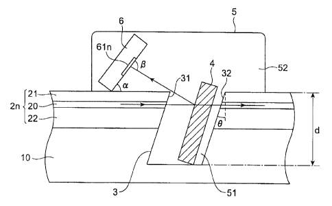
Fig. 2 is a cross-sectional view illustrating a
cross-sectional structure of the optical waveguide
module shown in Fig. 1 along the direction of the
optical axis of the optical waveguide 2~ (n = 1,
8) (the direction of optical transmission in the
planar-waveguide-type optical circuit 1). In Fig. 2,
a portion including the groove 3, reflection filter
4, and photodetector array 6 is shown in an enlarged
form.
As shown in Fig. 2, the optical waveguides 2"
in the planar-waveguide-type optical circuit 1 are
configured by forming a lower cladding 22, core 20,
and upper cladding 21 on the substrate 10. The
groove 3 traversing the optical waveguides 2n at the
predetermined position is formed at a depth d which
spans at least a region, corresponding to the core
20, through which the signal light propagated in the
optical waveguide 2" passes. In addition, this
11
CA 02453783 2004-O1-14
groove 3 is formed obliquely at a predetermined tilt
angle 8 (0° < 8) relative to the vertical axis
orthogonal to the optical axis of the optical
waveguide 2n (orthogonal to the substrate 10).
In the present embodiment, the depth d of the
groove 3 is set to be greater than the thickness of
the optical waveguide 2" down to the lower cladding
22, and part of a lower portion of the groove 3 is
formed by removing a predetermined region of the
substrate 10. Here, the inner wall portion of the
groove 3 in the optical circuit 1 is composed of the
core 20, claddings 21 and 22, and substrate 10.
Inside the groove 3, the reflection filter 4 is
inserted. The reflection filter 4 is placed at an
angle 8 substantially identical to that of the
groove 3 to span at least a region through which the
signal light propagated in the optical waveguide 2n
passes. This reflection filter 4 is preferably made
of a dielectric multilayer film filter, which
reflects part of the signal light propagated in the
optical waveguide 2n having a wavelength within a
predetermined signal light wavelength band at a
predetermined reflectance.
At a predetermined position on the upper
surface side of the upper cladding 21 of the planar
waveguide-type optical circuit l, the photodetector
12
CA 02453783 2004-O1-14
array 6 is placed which has photodetectors 61~ (n -
1, ..., 8) each corresponding to one of the optical
waveguides 2~. This photodetector array 6 is placed
so that each reflected light, which is part of the
signal light propagated in the optical waveguide 2n
reflected by the reflection filter 4, is incident on
a light-receiving surface of the corresponding
photodetector 61~.
In the present embodiment, the photodetector
array 6 is placed so that its light-receiving
surface makes an oblique angle a (0° < a < 90°)
relative to the upper surface of the planar-
waveguide-type optical circuit 1. This angle a is
preferably set so that the reflected light from the
reflection filter 9 is incident on the light-
receiving surface of the photodetector 61~ at a
substantially orthogonal angle ~. In the
configuration example shown in Fig. 2, a front-
surface-incident-type photodiode is used for the
photodetector 61~ of the photodetector array 6. The
surface of the photodetector array 6 facing the
reflection filter 4 is the light-receiving surface
on which the reflected light from the reflection
filter 4 is incident.
?5 The light-receiving surface of the
photodetector 61~ is provided with an anti-reflection
13
CA 02453783 2004-O1-14
coating (AR coating), which is a coating film
preventing reflection of light within a
predetermined wavelength band corresponding to the
signal light wavelength band of the signal light
propagated in the optical waveguide 2".
The inside of the groove 3 including the
reflection filter 9 is sealed with the filling resin
5. fihis filling resin 5 serves as filter fixing
resin for fixing the reflection filter 4 placed
inside the groove 3. The filter fixing resin 5 is
preferably made with resin material having a
refractive index substantially identical to that of
the core 20 of the optical waveguide 2~ through which
the signal light is propagated.
The filter fixing resin 5 in the present
embodiment is composed of an inner filling resin
portion 51 sealing the inside of the groove 3 and an
upper filling resin portion 52 sealing a
predetermined range on the upper surface side of the
planar-waveguide-type optical circuit 1 including
the upper portion of the groove 3: The inner
filling resin portion 51 and upper filling resin
portion 52 are integrally formed with identical
resin material. In general, the filter fixing resin
,''S is formed such that it fills at least the inside of
the groove for seal thereof.
14
CA 02453783 2004-O1-14
The upper filling resin portion 52 is provided
in a range including at least the light-receiving
surface of the photodetector array 6. As a result,
between the reflection filter 4 for reflecting part
of the signal light and the photodetector 61~ for
detecting the reflected light from the reflection
filter 4, the reflected light path along which the
reflected light propagates is filled with the filter
fixing resin 5.
Here, the groove 3 for inserting the reflection
filter 4 provided in the planar-waveguide-type
optical circuit 1 is formed with material having a
refractive index substantially identical to that of
the core 20 of the optical waveguide 2~ and the
filter fixing resin 5 with respect to the signal
light having a wavelength within the signal light
wavelength band. Specifically, in the groove 3
shown in Fig. 2, which has an inner wall portion
composed of the core 20, claddings 21 and 22, and
substrate 10, a glass substrate made of glass
material having a refractive index substantially
identical to that of the core 20 of the optical
waveguide 2n and the filter fixing resin 5 is used
for the substrate 10 constituting part of the groove
?5 3. In general, the refractive index difference
between the core 20 and the claddings 21 and 22 is
CA 02453783 2004-O1-14
sufficiently small.
In the above configuration, when the signal
light of a predetermined wavelength propagated in
the optical waveguide 2" on the input end 11 side is
emitted via an upstream end surface 31 to the inner
filling resin portion 51 in the groove 3, part of
the signal light is reflected obliquely upward with
respect to the planar-waveguide-type optical circuit
1 at a predetermined reflectance by the reflection
filter 4 placed obliquely relative to the optical
axis. The other signal light components are
transmitted through the inner filling resin portion
51 and reflection filter 4 .and incident via a
downstream end surface 32 on the optical waveguide 2~
at the output end 12 side.
On the other hand, the reflected light
reflected by the reflection filter 9 passes through
the inner filling resin portion 51 and upper filling
resin portion 52 to reach the photodetector array 6,
and is incident on its light-receiving surface into
the photodetector 61" at the predetermined incident
angle (3_ The light intensity of the reflected light
detected by the photodetector 61" is then used to
monitor the light intensity of the signal light
?5 propagated in the optical waveguide 2".
The effect of the optical waveguide module of
16
CA 02453783 2004-O1-14
the present embodiment will now be described.
In the optical waveguide module shown in Figs.
1 and 2, the signal light propagated in the optical
waveguide 2n provided in the optical circuit 1 is not
split by an optical coupler or the like. Rather, in
the configuration of the optical waveguide module,
part of the signal light is reflected by the
reflection filter 4 placed in the groove 3 provided
on the optical waveguide 2~, and the reflected light
can be monitored by means of the light intensity of
the signal light_ This simplifies the configuration
and manufacturing process of the optical circuit.
Furthermore, the material for each region
constituting the groove 3 provided in the planar
waveguide-type optical circuit 1 for inserting the
reflection filter 4, is to be made with material
having a refractive index substantially identical to
that of the core 20 of the optical waveguide 2" and
the filter fixing resin 5 filling the inside of the
groove 3. As a result, reflection of light is
inhibited at such regions as the inner wall portion
of the groove 3 formed in the optical circuit 1
including the optical waveguides 21-28, the filter
fixing resin 5, and their interfaces, and thereby
?5 generation of extra scattered light inside the
groove 3 is reduced. Therefore, she optical
17
CA 02453783 2004-O1-14
waveguide module capable of enhancing the monitoring
characteristics for the signal light is obtained.
As a specific configuration for such a groove 3,
in the example presented in the above embodiment, a
substrate made of material having a refractive index
substantially identical to that of the core 20 of
the optical waveguide 2" and the filter fixing resin
5 is used for the substrate 10 constituting a
portion of the groove 3. By configuring the optical
circuit 1 with the substrate 10 made of . such
material, the groove 3 satisfying the above
conditions can be readily formed in the planar-
waveguide-type optical circuit 1.
The material forming the groove 3 in the
optical circuit 1 is made with glass material having
a refractive index substantially identical to that
of the core 20 of the optical waveguide 2" and the
filter fixing resin 5 as the material for the
substratell0. By using glass material having good
workability and being inexpensive as described above,
the optical waveguide module can be fabricated at a
low cost. Alternatively, material other than glass
material may be used. If any member other than the
substrate constitutes the groove, it is preferable
to use material having a refractive index
substantially identical to that of the core of the
18
CA 02453783 2004-O1-14
optical waveguide and the filter fixing resin as the
material for such a member, as with the substrate 10
described above.
Furthermore, as shown in Fig. 2, the groove 3
formed in the optical circuit 1 is preferably formed
obliquely at a predetermined tilt angle 8 relative
to the vertical axis orthogonal to the optical axis
of the optical waveguide 2n. As a result, the
configuration is suitably realized for monitoring
the light intensity of the signal light by detecting
the reflected light from the reflection filter 4
with the photodetector 61~. In this case, as the
reflection filter 4 for reflecting part of the
signal light, it is preferable to use a reflection
filter which achieves polarization compensation to
allow the reflectances for the two orthogonal
polarizations to be substantially equal.
As an optical circuit in which optical
waveguides~ are provided on its substrate and a
groove for inserting a reflection filter is formed,
Figs. 1 and 2 show the planar-waveguide-type optical
circuit 1 made with the planar-waveguide-type
optical waveguides 2". However, optical circuits
having other configurations may be used. For
:~5 example, an optical circuit configured by fixing
optical fibers as optical waveguides in a fixing V-
19
CA 02453783 2004-O1-14
groove formed on the substrate, or an optical
circuit configured with planar-waveguide-type
optical waveguides in combination with optical
fibers, may be used.
The configuration and effect of the optical
waveguide module shown in Figs_ 1 and 2 will be
described more specifically.
Figs. 3A and 3B are (A) a plan view and (B) a
cross-sectional view illustrating an example of the
configuration of the optical waveguide module. This
optical waveguide module is shown for the purpose of
describing the effect of the optical waveguide
module shown in Figs. 1 and 2. The plan view of Fig.
3A and the cross-sectional view of Fig. 3B
correspond to the plan view of Fig. 1 and the cross-
sectional view of Fig. 2, respectively.
The optical wave guide module shown in Figs . 3A
and 3B is composed of a planar-waveguide-type
optical circuit 9 in which eight planar-waveguide-
type optical waveguides 92 and a groove 93 are
provided on its substrate 90, a reflection filter 94
placed inside the groove 93, filter fixing resin 95,
a submount substrate 97, and a photodetector array
96 placed on the filter fixing resin 95 and submount
substrate 97. In the present configuration example,
a Si (silicon) substrate is used for the substrate
CA 02453783 2004-O1-14
90 of the optical circuit 9 constituting a portion
of the groove 93.
Fig. 4 is a graph illustrating a light
intensity distribution in the optical waveguide
module shown in Figs. 3A and 3B. This graph shows
the spread of scattered light in the direction of
the groove 93 when signal light is inputted to a
particular channel in the eight-channel optical
waveguide module having the above configuration.
In this graph, the horizontal axis indicates an
amount of displacement (um~ in the direction of the
groove from the optical waveguide of the channel to
which the signal light is inputted. The vertical
axis indicates the light intensity detected at each
position as the photodetector is displaced in the
direction of the groove, in terms of its loss (dB)
where the light intensity of the inputted signal
light is used as a reference.
With regard to specific conditions, the optical
waveguide 92 is made with a planar-waveguide-type
optical wave guide with ~n - 0. 4 0, and the groove 93
has a width of 25 um and a tilt of A - 10°. The
reflection filter 94 is made with a polyimide
substrate-based reflection filter with a thickness
of 20 um. The photodetector array 96 for detecting
the reflected light is made with an eight-channel
21
CA 02453783 2004-O1-14
photodiode array in which front-surface-incident-
type photodiodes having a light-receiving area of
120 X 200 um are arranged. The distance from the
reflection point at the reflection filter 94 to the
light-receiving surface of the photodetector array
96 is set to 700 um.
Referring to the graph shown in Fig. 4, in the
region RO where the amount of displacement ranges
from -100 um to 100 um centered at the optical
waveguide of the channel to which the signal light
is inputted, a light intensity distribution of
substantially Gaussian shape is obtained
corresponding to the light intensity distribution of
the signal light itself. On the other hand, in the
outside regions R1 and R2, the detected light
intensity does not decrease sufficiently, leaving
some level of light intensity in a wide range. For
example, if photodiodes of adjacent channels are
spaced apart by 250 um, the crosstalk in these
channels will be on the order of 38 dB. Here, the
crosstalk between channels is represented by a ratio
of the light intensity detected in a channel other
than the normal channel to that detected in the
normal channel.
?5 The extra residual light intensity distribution
in such outside regions R1 and R2, and the resultant
22
CA 02453783 2004-O1-14
degradation of S/N ratio in the photodetectors, or
degradation of crosstalk between adjacent channels,
may be caused by generation of extra scattered light
inside the groove for inserting the reflection
filter. Fig. 5 is a schematic view illustrating the
generation of scattered light in the optical
waveguide module.
More specifically, in the optical waveguide
module shown in Figs. 3A and 3B which uses a Si
substrate for the substrate of the optical circuit,
the regions constituting the groove have
approximately the following refractive indices, n: n
- 1.46 for quartz-based optical waveguides such as
planar-waveguide-type optical waveguides or optical
fibers; n - 1.6 for the polyimide-substrate-based
reflection filter; and n = 3.46 for the Si substrate
of the optical circuit. In such a configuration,
the difference of refractive indices in various
regions of the groove will cause reflection of light
at their interfaces. For example, the Si substrate
is substantially transparent to the signal light in
the wavelength band of A = 1.55 um used as a signal
light wavelength band for communication. However,
the difference of the refractive index compared to
the other regions such as the filter fixing resin
causes extra reflection of light at its interface.
23
CA 02453783 2004-O1-14
Furthermore, in the above configuration where
the inside of the groove is filled with resin for
fixing the reflection filter, the scattered light
generated inside the groove is reflected at the
interface with the Si substrate and the like of
higher refractive indices, and at the same time, as
shown schematically in Fig. 5 by dashed lines, the
scattered light is confined in the periphery of the
reflection filter and diffused inside the groove in
the direction of the groove. The scattered light
inside the groove is also generated by surface
roughness of the inner wall of the groove,
refraction of light in the reflection filter,
coupling loss caused by the signal light reentering
the optical waveguide from the downstream end
surface of the groove, reflection of light at the
light-receiving surface of the photodetectors, and
the like. Such scattered light is confined as well
in the periphery of the reflection filter and
diffused in the direction of the groove.
On the contrary, in the optical waveguide
module shown in Figs. 1 and 2, the optical circuit 1
is configured with the substrate 10 made of material
such as glass material having a refractive index
?.5 substantially identical to that of the core 20 of
the optical waveguide 2" and the filter fixing resin
24
CA 02453783 2004-O1-14
5. In this optical circuit l, the groove 3 for
inserting the reflection filter 4 is formed.
As a result, since the difference of refractive
indices at the interface of various regions of the
groove 3 is reduced, the generation of extra
scattered light due to reflection of light at the
interface or otherwise is inhibited. The
confinement of scattered light inside the groove 3,
and its diffusion in the direction of the groove are
inhibited as well. This results in preventing
degradation of monitoring characteristics for the
signal light, such as the S/N ratio at the
photodetectors and the crosstalk between adjacent
channels, caused by the scattered light generated
inside the groove 3, thereby enhancing the
monitoring characteristics.
Figs. 6A and 6B are graphs illustrating light
intensity distributions in the optical waveguide
module shown in Figs. 1 and 2. Here, Fig. 6A shows
a graph of a light intensity distribution where the
substrate of the optical circuit in the
configuration shown in Fig. 1 is replaced with a Si
substrate. Fig. 6B shows a graph of a light
intensity distribution where the quartz glass
substrate is used as described above. Each of these
graphs shows the spread of scattered light in the
CA 02453783 2004-O1-14
direction of the groove 3 when signal light is
inputted to a particular channel in the eight-
channel optical waveguide module having the
configuration shown in Fig. 1.
In these graphs, the horizontal axis indicates
an amount of displacement (um) in the direction of
the groove from the optical waveguide 2~ of the
channel to which the signal light is inputted. The
vertical axis indicates the light intensity detected
at each position as the photodetector is displaced
in the direction of the groove, in terms of its loss
(dB) where the light intensity of the inputted
signal light is used as a reference.
With regard to specific conditions, except for
the Si substrate and quartz glass substrate
described above, the optical waveguide module has
the same configuration in each case of Figs. 6A and
6B. The material for the filter fixing resin 5 is
made with organic silicone-based resin with a
refractive index n - 1.48. Here, outside this
filter fixing resin 5, scattered light reducing
resin (not shown in Figs. 1 and 2) made with UV
acrylic resin having a refractive index of n - 1.53
is provided. Regarding the optical waveguide 2n,
reflection filter 4 and others, the conditions are
the same as those described above with reference to
26
CA 02453783 2004-O1-14
Fig. 9.
As shown in Fig. 6A, for the optical waveguide
module where a Si substrate with a high refractive
index is used as the substrate constituting a
portion of the groove, in the region SO including
the channel to which the signal light is inputted, a
light intensity distribution of substantially
Gaussian shape is obtained corresponding to the
light intensity distribution of the signal light
itself. On the other hand, in such a configuration,
extra scattered light is generated inside the groove
3 in which the reflection filter 4 is placed,
confined inside the groove 3, and diffused toward
the periphery in the direction of the groove. Here,
while the light intensity of the scattered light
detected by the photodetector of the channel to
which the signal light is inputted decreases, some
level of light intensity remains in a wide range of
the outside regions S1 and S2.
On the contrary, as shown in Fig. 6B, in the
optical waveguide module where a quartz glass
substrate having a refractive index substantially
identical to that of the core 20 of the optical
waveguide 2~ and the filter fixing resin 5 is used as
the substrate constituting a portion of the groove,
generation of scattered light inside the groove 3,
27
CA 02453783 2004-O1-14
and its confinement and diffusion in the direction
of the groove are inhibited. As a result, the light
intensity of the scattered light remaining in the
outside regions 51 and S2 is reduced, and the
crosstalk in the adjacent channels is inhibited
below 40 dB. Accordingly, the monitoring
characteristics for the light intensity of the
signal light by the optical waveguide module are
enhanced.
Fig. 7 is a plan view illustrating the
configuration of a second embodiment of the optical
waveguide module. This optical waveguide module
comprises a planar-waveguide-type optical circuit 1
composed of a substrate 10 and planar-waveguide-type
optical waveguides 21-28 provided on the substrate 10.
The configuration of the present optical
waveguide module is the same as the optical
waveguide module shown in Figs. 1 and 2 with respect
to the optical waveguides 21-28 and groove 3 of the
planar-waveguide-type optical circuit 1, the filter
fixing resin 5, and the photodetector array 6 having
photodetectors 611-618. The cross-sectional
structure along the optical axis of the optical
waveguide module at a position including the optical
waveguide 2n is the same as that shown in Fig. 2 for
the first embodiment. Note that, in Fig. 7, the
28
CA 02453783 2004-O1-14
filter fixing resin 5 composed of the inner filling
resin portion 51 and upper filling resin portion 52
is not shown for visual simplicity.
In the present embodiment, eight reflection
filters 911-41e are placed inside the groove 3
corresponding to the eight optical waveguides 2,-2a,
respectively, as the reflection filter for
reflecting part of signal light propagated in each
of the optical waveguides 21-28 at a predetermined
reflectance.
Figs. 8A and 8B are cross-sectional views along
(A) the I-I arrow and (B) the II-II arrow
illustrating the cross-sectional structures of the
optical waveguide module shown in Fig. 7 along the
direction perpendicular to the optical axis of the
optical waveguide 2n (n = 1, ..., 8). Here, Fig. 8A
is a cross-sectional view illustrating the structure
of the optical waveguide 2" at a position, as shown
in Fig. 7, where the groove 3 and filter fixing
resin 5 are not provided. Fig. 8B is a cross-
sectional view illustrating the configuration inside
the groove 3 such as the reflection filter 91" at a
position where the groove 3 and filter fixing resin
5 are provided.
Each of the reflection filters 41~ (n = 1, _..,
8) is placed at a tilt angle 8 substantially
29
CA 02453783 2004-O1-14
identical to that of the groove 3 to span at least a
region through which the signal light propagated in
the optical waveguide 2~ passes. This reflection
filter 41n is preferably made of a dielectric
multilayer film filter, which reflects part of the
signal light propagated in the optical waveguide 2"
having a wavelength within a predetermined signal
light wavelength band at a predetermined reflectance.
Furthermore, between each pair of the eight
reflection filters 41i-418 inside the groove 3, a
light blocking layer 7 made of light blocking
material is provided. The light blocking layer 7 is
also provided between the reflection filter 411, 418
located at either end and the corresponding end of
the groove 3. As a result, inside the groove 3, as
shown in Fig. 8B, the reflection filters 41n and
light blocking layers 7 are provided alternately
along the direction of the groove. The light
blocking material for the light blocking layer 7 is
made with, for example, light absorbing material for
absorbing light having a wavelength in the signal
light wavelength band.
At a predetermined position on the upper
surface side of the upper cladding 21 of the planar-
waveguide-type optical circuit l, the photodetector
array 6 is placed which has photodetectors 61~ (n -
CA 02453783 2004-O1-14
l, ..., 8) each corresponding to one of the optical
waveguides 2~ and reflection filters 41~. This
photodetector array 6 is placed so that each
reflected light, which is part of the signal light
propagated in the optical waveguide 2~ reflected by
the reflection filter 41~, is incident on a light-
receiving surface of the corresponding photodetector
61n.
In the optical waveguide module of the present
embodiment, as with the first embodiment, the
substrate 10 constituting a portion of the groove 3
provided in the optical circuit 1 for inserting the
reflection filter 4 is made with a substrate made of
material having a refractive index substantially
identical to that of the core 20 of the optical
waveguide 2~ and the filter fixing resin 5. As a
result, reflection of light is inhibited at such
regions as the inner wall portion of the groove 3
formed in the optical circuit 1 including the
optical waveguides 21-2B, the filter fixing resin 5,
and their interfaces, and thereby generation of
extra scattered light inside the groove 3 is reduced.
Therefore, the optical waveguide module capable of
enhancing the monitoring characteristics for the
signal light is obtained.
Furthermore, for the eight optical waveguides
31
CA 02453783 2004-O1-14
21-28 provided in the optical circuit 1, eight
reflection filters 411-41a corresponding to the
optical waveguides 21-28, respectively, and the light
blocking layers 7 are alternately provided. Here,
even if some level of extra scattered light is
generated inside the groove 3, diffusion of the
scattered light in the direction of the groove is
prevented by the light blocking layers 7. As a
result, since generation of crosstalk between
adjacent channels is inhibited, the monitoring
characteristics for the signal light can be further
enhanced. Such a configuration may be applied in
general to an optical waveguide module having N
(where N is greater than one) optical waveguides.
Figs. 9A-9C, 10A and lOB are process diagrams
illustrating schematically an example of a method of
manufacturing the optical waveguide module shown in
Figs. 7, 8A and 8B. Here, in Figs. 9A-9C, each
process step is illustrated by a cross-sectional
view along the optical axis (see Fig. 2). In Figs.
10A and 10B, each process step is illustrated by a
plan view (see Fig. 1).
First, in a planar-waveguide-type optical
circuit 1 in which core 20 and claddings 21 and 22
constituting optical waveguides 2n are formed on a
substrate 10 made of material such as quartz glass,
32
CA 02453783 2004-O1-14
a groove 3 traversing the optical waveguides 21-2B is
formed by RIE etching at a predetermined position
along the direction of optical transmission (Fig.
9A). Next, on the upper surface side of the optical
circuit 1 including the groove 3, a Ge-doped glass
layer 70 doped with a high concentration of Ge
(germanium) is formed by the FHD method (Fig. 9B).
Here, Ge is a dopant having a light absorbing
effect, and the Ge-doped glass layer 70 described
above is a glass layer which can be used as a light
blocking layer. The doping rate of Ge in the Ge-
doped glass layer 70 is set, for example, to
approximately 9 wto (weight o). Subsequently, the
Ge-doped glass layer 70 is etched back except for
the portion formed inside the groove 3 to expose the
upper surface of the optical circuit 1 (Fig. 9C).
Next, portions of the Ge-doped glass layer 70
left inside the groove 3 after the etch back which
remain on the optical waveguides 21-28 are removed by
RIE etching to form light blocking layers 7 (Fig.
10A). Then, inside the groove 3 from which the Ge-
doped glass layer is removed, reflection filters 411-
41e corresponding to the optical waveguides 21-28 are
inserted, respectively (Fig. 10B). By further
forrcting filter fixing resin 5, placing a
photodetector array 6 and so north, the optical
33
CA 02453783 2004-O1-14
waveguide module of the configuration shown in Figs.
7, 8A and 8B can be fabricated.
The optical waveguide module according to the
present invention is not limited to the embodiments
described above, but various modifications may be
made. For example, for the configuration and
placing method of the photodetector for detecting
the reflected light from the reflection filter,
various configurations other than the configuration
example shown in Figs. 1 and 2 may be used. For
example, as shown in Figs. 3A and 3B, a
configuration may be used in which the photodetector
array is placed on a submount substrate.
Suitable embodiments of the optical waveguide
module according to the present invention will be
further described.
Fig_ 11 is a plan view illustrating the
configuration of a third embodiment of the optical
waveguide module according to the present invention.
This optical waveguide module comprises an optical
circuit 101 configured to have a substrate 110 and
eight (eight channels of) optical waveguides 1021-
1028 provided on the substrate 110. The present
embodiment uses planar-waveguide-type optical
waveguides formed on the substrate 110 as the
optical wave guides 1021-102. As the substrate 110,
34
CA 02453783 2004-O1-14
r
a Si (silicon) substrate is used, for example.
Each of the optical waveguides 1021-1028 is
formed along a predetermined direction of optical
transmission (in the direction of the arrow shown in
Fig. 11) from an input end 111 toward an output end
112 of the planar-waveguide-type optical circuit 101,
in parallel and equally spaced relative to each
other. At a predetermined position along the
direction of optical transmission of the planar-
waveguide-type optical circuit 101, a groove 103
traversing the optical waveguides 1021-1028 is formed.
Inside the groove 103 of the optical circuit
101, a reflection filter 104 is placed which
reflects part of signal light propagated in each of
the optical waveguides 1021-1028 at a predetermined
reflectance. The inside of the groove 103 is sealed
with filling resin 105. At a position upstream of
the groove 103 along the direction of optical
transmission and on the upper surface side of the
planar-waveguide-type optical circuit 101, a
photodetector array 106 is placed. This
photodetector array 106 has eight photodetectors
1611-1616 corresponding to the eight optical
waveguides 1021-1028 provided in the planar
waveguide-type optical circuit 101, respectively.
Fig. 12 is a cross-sectional view illustrating
CA 02453783 2004-O1-14
a cross-sectional structure of the optical waveguide
module shown in Fig. 11 along the direction of the
optical axis of the optical waveguide 102n (n -
1, ..., B) (the direction of optical transmission in
the planar-waveguide-type optical circuit 101). In
Fig. 12, a portion including the groove 103,
reflection filter 104, and photodetector array 106
is shown in an enlarged form.
As shown in Fig. 12, the optical waveguides
102 in the planar-waveguide-type optical circuit 101
are configured by forming a lower cladding 122, core
120, and upper cladding 121 on the substrate 110.
The groove 103 traversing the optical waveguides 102
at the predetermined position is formed at a depth d
which spans at least a region, corresponding to the
core 120, through which the signal light propagated
in the optical waveguide 102n passes. In addition,
this groove 103 is formed obliquely at a
predetermined tilt angle A (0° < 8) relative to the
vertical axis orthogonal to the optical axis of the
optical waveguide 102" (orthogonal to the substrate
110) .
In the present embodiment, the depth d of the
groove 103 is set to be greater than the thickness
of the optical waveguide 102 down to tre lower
cladding 122, and part of a lower portion of the
36
CA 02453783 2004-O1-14
groove 103 is formed by removing a predetermined
region of the substrate 110 made of a Si substrate
and the like. Here, the inner wall portion of the
groove 103 in the optical circuit 101 is composed of
the core 120, claddings 121 and 122, and substrate
110.
Inside the groove 103, the reflection filter
109 is inserted. The reflection filter 109 is
placed at a tilt angle 8 substantially identical to
that of the groove 103 to span at least a region
through which the signal light propagated in the
optical waveguide 102n passes. This reflection
filter 104 is preferably made of a dielectric
multilayer film filter, which reflects part of the
signal light propagated in the optical waveguide 102n
having a wavelength within a predetermined signal
light wavelength band at a predetermined reflectance.
At a predetermined position on the upper
surface side of the upper cladding 121 of the
planar-waveguide-type optical circuit 101, the
photodetector array 106 is placed which has
photodetectors 161 (n - l, ..., 8) each
corresponding to one of the optical waveguides 102n.
This photodetector array 106 is placed so that each
reflected light, which is part of the signal light
propagated in the optical waveguide 102n reflected by
37
CA 02453783 2004-O1-14
the reflection filter 109, is incident on a light-
receiving surface of the corresponding photodetector
161" _
In the present embodiment, the photodetector
array 106 is placed so that its light-receiving
surface makes an oblique angle a (0° < a < 90°)
relative to the upper surface of the planar-
waveguide-type optical circuit 101. This angle a is
preferably set so that the reflected light from the
reflection filter 104 is incident on the light-
receiving surface of the photodetector 161 at a
substantially orthogonal angle Vii. In the
configuration example shown in Fig. 12, a front-
surface-incident-type photodiode is used for the
photodetector 161 of the photodetector array 106.
The surface of the photodetector array 106 facing
the reflection filter 104 is the light-receiving
surface on which the reflected light from the
reflection filter 104 is incident.
The light-receiving surface of the
photodetector 161" is provided with an AR coating,
which is a coating film preventing reflection of
light within a- predetermined wavelength band
corresponding to the signal light wavelength band of
:'S the signal light propagated in the optical waveguide
102T,.
38
CA 02453783 2004-O1-14
The inside of the groove 103 including the
reflection filter 104 is sealed with the filling
resin 105. This filling resin 105 serves as filter
fixing resin for fixing the reflection filter 104
placed inside the groove 103. The filter fixing
resin 105 is formed with resin material having a
higher refractive index than that of the core 120 of
the optical waveguide 102 with respect to the signal
light having a wavelength in the signal light
wavelength band.
The filter fixing resin 105 in the present
embodiment is composed of an inner filling resin
portion 151 sealing the inside of the groove 103 and
an upper filling resin portion 152 sealing a
predetermined range on the upper surface side of the
planar-waveguide-type optical circuit 101 including
the upper portion of the groove 103. The inner
filling resin portion 151 and upper filling resin
portion 152 are integrally formed with identical
resin material. In general, the filter fixing resin
is formed such that it fills at least the inside of
the groove for seal thereof.
The upper filling resin portion 152 is provided
in a range including at least the light-receiving
surface of the photodetector array 106. As a result,
between the reflection filter 104 for reflecting
39
CA 02453783 2004-O1-14
part of the signal light and the photodetector 161n
for detecting the reflected light from the
reflection filter 104, the reflected light path
along which the reflected light propagates is filled
with the filter fixing resin 105.
In the above configuration, when the signal
light of a predetermined wavelength propagated in
the optical waveguide 102 on the input end 111 side
is emitted via an upstream end surface 131 to the
inner filling resin portion 151 in the groove 103,
part of the signal light is reflected obliquely
upward with respect to the planar-waveguide-type
optical circuit 101 at a predetermined reflectance
by the reflection filter 104 placed obliquely
relative to the optical axis. The other signal
light components are transmitted through the inner
filling resin portion 151 and reflection filter 104
and incident via a downstream end surface 132 on the
optical waveguide 102 at the output end 112 side.
On the other hand, the reflected light
reflected by the reflection filter 104 passes
through the inner filling resin portion 151 and
upper filling resin portion 152 to reach the
photodetector array 106, and is incident on its
light-receiving surface into the photodetector 161
at the predetermined incident angle ~. The light
CA 02453783 2004-O1-14
intensity of the reflected light detected by the
photodetector 161 is then used to monitor the light
intensity of the signal light propagated in the
optical waveguide 102.
S The effect of the optical waveguide module of
the present embodiment will now be described.
In the optical waveguide module shown in Figs.
11 and 12, the signal light propagated in the
optical waveguide 102 provided in the optical
circuit 101 is not split by an optical coupler or
the like. Rather, in the configuration of the
optical waveguide module, part of the signal light
is reflected by the reflection filter 104 placed in
the groove 103 provided on the optical waveguide 102n,
and the reflected light can be monitored by means of
the light intensity of the signal light. This
simplifies the configuration and manufacturing
process of the optical circuit.
Furthermore, the filter fixing resin 105
filling the inside of the groove 103 which is
provided in the planar-waveguide-type optical
circuit 101 and in which the reflection filter 104
is inserted, is to be made with resin material
having a higher refractive index than that of the
core 120 of the optical waveguide 102. As a result,
scattered light generated inside the groove 103 is
41
CA 02453783 2004-O1-14
actively emitted outside, and thereby confinement
and diffusion of extra scattered light inside the
groove 103 is inhibited as described below.
Therefore, influence of the extra scattered light is
reduced and the optical waveguide module capable of
enhancing the monitoring characteristics for the
signal light is obtained.
Here, regarding the resin material for the
filter fixing resin 105, it is preferable to use
resin material which does not contain particles of
dimensions substantially identical (or comparable)
to the wavelength in the signal light wavelength
band. If resin material containing filler particles
having dimensions comparable to the wavelength of
the signal light for communication is used as the
filter fixing resin 105, scattering of light occurs
by the filler particles inside the filter fixing
resin 105, which results in increasing extra
scattered light inside the filter fixing resin 105.
On the contrary, by using resin material which does
not contain filler particles of such dimensions,
scattering of light inside the filter fixing resin
105 is inhibited from occurring.
Furthermore, as shown in Fig. 12, the groove
103 formed in the optical circuit 101 is preferably
formed obliquely at a predetermined tilt angle B
92
CA 02453783 2004-O1-14
relative to the vertical axis orthogonal to the
optical axis of the optical waveguide 102. As a
result, a configuration is suitably realized for
monitoring the light intensity of the signal light
by detecting the reflected light from the reflection
filter 104 with the photodetector 161. In this case,
as the reflection filter 104 for reflecting part of
the signal light, it is preferable to use a
reflection filter which achieves polarization
compensation to allow the reflectances for the two
orthogonal polarizations to be substantially equal.
As an optical circuit in which optical
waveguides are provided on its substrate and a
groove for inserting a reflection filter is formed,
Figs. 11 and 12 show the planar-waveguide-type
optical circuit 1 made with the planar-waveguide-
type optical waveguides 102. However, optical
circuits having other configurations may be used.
For example, an optical circuit configured by fixing
optical fibers as optical waveguides in a fixing V-
groove formed on the substrate, or an optical
circuit configured with planar-waveguide-type
optical waveguides in combination with optical
fibers, may be used.
The configuration and effect of the optical
waveguide module shown in Figs. 11 and 12 will be
43
CA 02453783 2004-O1-14
described more specifically.
As described above, Figs. 3A and 3B are (A) a
plan view and (B) a cross-sectional view
illustrating an example of the configuration of the
optical waveguide module. Fig. 4 is a graph
illustrating a light intensity distribution in the
optical waveguide module shown in Figs. 3A and 3B.
Referring to the graph shown in Fig. 4, as
described above, in the region R0, a light intensity
distribution of substantially Gaussian shape is
obtained corresponding to the light intensity
distribution of the signal light itself. On the
other hand, in the outside regions Rl and R2, the
detected light intensity does not decrease
sufficiently, leaving some level of light intensity
in a wide range. For example, if photodiodes of
adjacent channels are spaced apart by 250 um, the
crosstalk in these channels will be on the order of
38 dB.
The extra residual light intensity distribution
in such outside regions R1 and R2, and the resultant
degradation of S/N ratio in the photodetectors, or
degradation of crosstalk between adjacent channels,
may be caused by generation of extra scattered light,
and its confinement and diffusion, inside the groove
for inserting the reflection filter. Fig. 13 is a
44
CA 02453783 2004-O1-14
schematic view illustrating the generation of
scattered light in the optical waveguide module.
More specifically, in the optical waveguide
module shown in Figs_ 3A and 3B, the regions
constituting the groove have approximately the
following refractive indices, n: n - 1.46 for
quartz-based optical waveguides; n - 1.6 for the
polyimide-substrate-based reflection filter; and n -
3.46 for the Si substrate of the optical circuit.
In such a configuration, the difference of
refractive indices in various regions of the groove
will cause reflection of light at their interfaces.
For example, the Si substrate is substantially
transparent to the signal light in the wavelength
band of ~ - 1.55 um used as a signal light
wavelength band for communication. However, the
difference of the refractive index compared to the
other regions such as the filter fixing resin causes
extra reflection of light at its interface.
Furthermore, in the above configuration where
the inside of the groove is filled with resin for
fixing the reflection filter, the scattered light
generated inside the groove is reflected at the
interface with the inner wall portion of the groove
and the like, and at the same time, as shown
schematically in Fig. 13 by dashed lines, the
CA 02453783 2004-O1-14
scattered light is confined in the periphery of the
reflection filter and diffused inside the groove in
the direction of the groove. The scattered light
inside the groove is also generated by surface
roughness of the inner wall of the groove,
refraction of light in the reflection filter,
coupling loss caused by the signal light reentering
the optical waveguide from the downstream end
surface of the groove, reflection of light at the
light-receiving surface of the photodetectors, and
the like. Such scattered light is confined as well
in the periphery of the reflection filter and
diffused in the direction of the groove.
On the contrary, in the optical waveguide
module shown in Figs. 11 and 12, with regard to the
filter fixing resin 105 filling the groove 103 of
the optical circuit 101 in which the reflection
filter 104 is inserted, the filter fixing resin 105
is formed with resin material having a higher
refractive index than that of the core 120 of the
optical waveguide 102n.
As a result, even if any extra scattered light
is generated inside the groove 103, the scattered
light can be emitted out of the filter fixing resin
?5 105 filling the groove 103, so that the scattered
light ma y be actively let out . Here, the above-
46
CA 02453783 2004-O1-14
described confinement of scattered light inside the
groove 103, and its diffusion in the direction of
the groove are inhibited. This results in
preventing degradation of monitoring characteristics
for the signal light, such as the S/N ratio at the
photodetectors and the crosstalk between adjacent
channels, caused by the scattered light generated
inside the groove 103, thereby enhancing the
monitoring characteristics.
Fig. 14 is a graph illustrating a light
intensity distribution in the optical waveguide
module shown in Figs. 11 and 12. This graph shows
the spread of scattered light in the direction of
the groove 103 when signal light is inputted to a
particular channel in the eight-channel optical
waveguide module having the configuration shown in
Fig. 11.
In this graph, the horizontal axis indicates an
amount of displacement (um) in the direction of the
groove from the optical waveguide 102n of the channel
to which the signal light is inputted. The vertical
axis indicates the light intensity detected at each
position as the photodetector is displaced in the
direction of the groove, in terms of its loss (dB)
where the light intensity of the inputted signal
light is used as a reference.
47
CA 02453783 2004-O1-14
With regard to specific conditions, the
material for the filter fixing resin 105 is made
with organic silicone-based resin having a
refractive index n - 1.48, which is higher than the
refractive index of the core 120 of the optical
waveguide 102, n - 1.46. The substrate 110 of the
optical circuit 101 is made with a Si substrate.
Regarding the optical waveguide 102n, reflection
filter 104 and others, the conditions are the same
as those described above with reference to Fig. 4.
As shown in Fig. 14, in the optical. waveguide
module where resin material having a higher
refractive index than that of the core 120 of the
optical waveguide 102 is used as the filter fixing
resin 105, confinement of the scattered light
generated inside the groove 103 and its diffusion in
the direction of the groove are inhibited. This
results in reducing the light intensity of the
scattered light remaining in the outside regions
relative to the channel to which the signal light is
inputted, thereby enhancing the monitoring
characteristics for the light intensity of the
Signal light by the optical waveguide module. In
the example shown in Fig. 19, the crosstalk in the
adjacent channels is improved by approximately 5 dB.
Here, regarding the range where the filter
48
CA 02453783 2004-O1-14
fixing resin 105 is formed, in view of the function
of diffusing and emitting out the scattered light
generated inside the groove 103, the resin to be
formed into the filter fixing resin 105 is
preferably applied to a wide range. For example, as
shown in Fig_ 15, which shows a variation of the
configuration of the optical waveguide module shown
in Fig. 11, the filter fixing resin 105 may be
provided to fill the entire package of the optical
waveguide module by covering the optical circuit 101
and the like. However, if the filter fixing resin
105 is applied directly to the photodetector array
106, it is preferable to use resin material having a
low Young's modulus such as silicone-based resin.
In addition, Fig. 15 also shows a tape fiber
181 for signal light input connected to the input
end 111 of the optical circuit 101, and a tape fiber
182 for signal light output connected to the output
end 112.
Fig_ 16 is a plan view illustrating the
configuration of a fourth embodiment of the optical
waveguide module. This optical waveguide module
comprises a planar-waveguide-type optical circuit
101 configured to have a substrate 110 and planar-
waveguide-type optical waveguides 1021-102e provided
on the substrate 110.
49
CA 02453783 2004-O1-14
The configuration of the present optical
waveguide module is the same as the optical
waveguide module shown in Figs. 11 and 12 with
respect to the optical waveguides 1021-1028 and
groove 103 provided in the planar-waveguide-type
optical circuit 101, the reflection filter 104, and
the photodetector array 106 having photodetectors
1611-1618. In the present embodiment, scattered
light reducing resin 107 made of one layer of resin
is further provided outside the filter fixing resin
105.
Fig. 17 is a cross-sectional view illustrating
a cross-sectional structure of the optical waveguide
module shown in Fig. 16 along the direction of the
optical axis of the optical waveguide 102n. In Fig.
17, a portion including the groove 103, reflection
filter 104, and photodetector array 106 is shown in
an enlarged form.
The groove 103 traversing the optical
waveguides 102 at the predetermined position in the
planar-waveguide-type optical circuit 101 is formed
to a depth which is greater than the thickness of
the optical waveguide 102" down to the lower cladding
122, and obliquely at a predetermined tilt angle 8.
Here, the inner wall portion of the groove 103 in
the optical circuit 101 is composed of the core 120,
CA 02453783 2004-O1-14
claddings 121 and 122, and substrate 110.
Inside the groove 103, the reflection filter
104 is inserted. The reflection filter 104 is
placed at a tilt angle A substantially identical to
that of the groove 103 to span at least a region
through which the signal light propagated in the
optical waveguide 102 passes. This reflection
filter 104 is preferably made of a dielectric
multilayer film filter, which reflects part of the
signal light propagated in the optical waveguide 102n
having a wavelength within a predetermined signal
light wavelength band at a predetermined reflectance.
At a predetermined position on the upper
surface side of the upper cladding 121 of the
planar-waveguide-type optical circuit 101, the
photodetector array 106 is placed which has
photodetectors 161 each corresponding to one of the
optical waveguides 102. This photodetector array
106 is placed so that each reflected light, which is
part of the signal light propagated in the optical
waveguide 102 reflected by the reflection filter 104,
is incident on a light-receiving surface of the
corresponding photodetector 161r.
The light-receiving surface of the
photodetector 161 is provided with an AR coating,
which prevents reflection of light within a
51
CA 02453783 2004-O1-14
predetermined wavelength band corresponding to the
signal light wavelength band of the signal light
propagated in the optical waveguide 102.
The inside of the groove 103 including the
reflection filter 104 is sealed with the filling
resin 105. This filling resin 105 serves as filter
fixing resin for fixing the reflection filter 109
placed inside the groove 103. The filter fixing
resin 105 is formed with resin material having a
higher refractive index than that of the core 120 of
the optical waveguide 102n with respect to the signal
light having a wavelength in the signal light
wavelength band.
The filter fixing resin 105 in the present
embodiment is composed of an inner filling resin
portion 151 sealing the inside of the groove I03 and
an upper filling resin portion 152 sealing a
predetermined range on the upper surface side of the
planar-waveguide-type optical circuit 101 including
the upper portion of the groove 103. The inner
filling resin portion 151 and upper filling resin
portion 152 are integrally formed with identical
resin material. Here, the upper filling resin
portion 152 is provided in a range including at
least the light-receiving surface of the
photodetector array 106.
52
CA 02453783 2004-O1-14
Furthermore, one layer of scattered light
reducing resin 107 is provided outside the filter
fixing resin 105. This scattered light reducing
resin 107 is formed in a predetermined range on the
upper surface side of the planar-waveguide-type
optical circuit 101 to cover the upper filling resin
portion 152 of the filter fixing resin 105 and the
photodetector array 106. The scattered light
reducing resin 107 is formed with resin material
having a higher refractive index than that of the
filter fixing resin 105 with respect to the signal
light having a wavelength within the signal light
wavelength band.
In the optical waveguide module of the present
embodiment, as with the third embodiment, the filter
fixing resin 105 filling the inside of the groove
103 which is provided in the planar-waveguide-type
optical circuit 101 for inserting the reflection
filter 104, is made with resin material having a
higher refractive index than that of the core 120 of
the optical waveguide 102". As a result, scattered
light generated inside the groove 103 is actively
emitted outside, and thereby confinement and
diffusion of extra scattered light inside the groove
103 are inhibited. Therefore, influence of the
extra scattered light is reduced and the optical
53
CA 02453783 2004-O1-14
waveguide module capable of enhancing the monitoring
characteristics for the signal light is obtained.
Moreover, in addition to this filter fixing
resin 105, around its periphery, the scattered light
reducing resin 107 is provided as a resin layer made
with resin material having a higher refractive index
than that of the filter fixing resin 105. As a
result, the scattered light generated inside the
groove 103 is emitted outside more effectively, and
thereby the monitoring characteristics for the
signal light can be further enhanced.
Fig. 18 is a graph illustrating a light
intensity distribution in the optical waveguide
module shown in Figs. 16 and 17. This graph shows
the spread of scattered light in the direction of
the groove 103 when signal light is inputted to a
particular channel in the eight-channel optical
waveguide module having the configuration shown in
Fig. 16.
In this graph, the horizontal axis indicates an
amount of displacement (um) in the direction of the
groove from the optical waveguide 102n of the channel
to which the signal light is inputted. The vertical
axis indicates the light intensity detected at each
position as the photodetector is displaced in the
direction of the groove, in terms of its loss (dB)
54
CA 02453783 2004-O1-14
where the light intensity of the inputted signal
light is used as a reference.
With regard to specific conditions, the
material for the filter fixing resin 105 is made
with organic silicone-based resin having a
refractive index n - 1.48, which is higher than the
refractive index of the core 120 of the optical
waveguide 102n, n - 1.46. The material for the
scattered light reducing resin 107 is made with UV
acrylic resin which has a refractive index of n -
'1.53 being higher than the refractive index of this
filter fixing resin 105. The substrate 110 of the
optical circuit 101 is made with a Si substrate.
Regarding the optical waveguide 102n, reflection
filter 104 and others, the conditions are the same
as those described above with reference to Fig. 4.
As shown in Fig. 18, in the optical waveguide
module where resin material having a higher
refractive index than that of the core 120 of the
optical~waveguide 102 is used as the filter fixing
resin 105, and where more resin material having a
further higher refractive index than that of the
filter fixing resin 105 is used as the scattered
light reducing resin 107, confinement of the
scattered light generated inside the groove 103 and
its diffusion in the direction of the groove~ are
CA 02453783 2004-O1-14
inhibited as with the case shown in Fig. 14, and
thereby the monitoring characteristics for the light
intensity of the signal light is enhanced.
More specifically, in the configuration where
only the filter fixing resin 105 is provided, the
periphery of the filter fixing resin 105 is air,
which has a refractive index of 1, being lower than
that of the filter fixing resin 105. On the other
hand, by providing the above-described scattered
light reducing resin 107 around the periphery of the
filter fixing resin 105, the scattered light inside
the filter fixing resin 105 is effectively emitted
out to the scattered light reducing resin 107 and
its outside. In the example shown in Fig. 18, the
crosstalk in the adjacent channels is improved by
approximately 5 dB.
Here, regarding resin material used for the
scattered light reducing resin 107, various kinds of
material may be used provided that the above-
described conditions for the refractive index are
satisfied. For example, either of resin material
being transparent to light with a wavelength in the
signal light wavelength band, or light absorbing
resin material may be used.
Regarding the range where the scattered light
reducing resin 107 is formed, in view of the
56
CA 02453783 2004-O1-14
function of diffusing and emitting out the scattered
light generated inside the groove 103, it is
preferable to form the scattered light reducing
resin 107 in a wide range as with the filter fixing
resin 105 (see Fig. 15). Furthermore, for the
number of layers of the scattered light reducing
resin, in the configuration example shown in Figs.
16 and 17, one layer of scattered light reducing
resin 107 is provided around the periphery of the
filter fixing resin 105. However, a plurality of
resin layers may be provided. In this case, it is
preferable to provide a configuration where the
refractive indices are successively increased from
the filter fixing resin 105 side to the outside.
In the third embodiment shown in Figs. 11 and
12, and the fourth embodiment shown in Figs. 16 and
17, the planar-waveguide-type optical circuit 101 in
which the planar-waveguide-type optical waveguides
102" are formed on the substrate 110 is used as the
optical circuit in which the groove for inserting
the reflection filter is formed. This optical
circuit is not limited to the planar-waveguide-type
optical circuit. Rather, an optical circuit
configured with optical fibers in part or all of the
optical circuit portion may be used.
Figs. 19A and 19B are cross-sectional views
57
CA 02453783 2004-O1-14
each illustrating a cross-sectional structure of the
optical waveguide module along the direction
perpendicular to the optical axis of the optical
waveguide. Fig. 19A shows a cross-sectional
structure of the optical circuit where planar-
waveguide-type optical waveguides are used for the
optical waveguides. This corresponds to the cross-
sectional structure perpendicular to the optical
axis of the optical waveguide module shown in Figs.
11 and 12. Fig. 19B shows a cross-sectional
structure of the optical circuit where optical
fibers are used for the optical waveguides in place
of the planar-waveguide-type optical waveguides.
The optical circuit shown in Fig. 19A is
configured, as described above with reference to Fig.
12, by forming a lower cladding 122, core 120, and
upper cladding 121 on the substrate 110. On the
other hand, in the optical circuit shown in Fig. 19B,
V-grooves 115 functioning as optical fiber aligning
members are formed on the upper surface side of the
substrate 110 in parallel and equally spaced
relative to each other. An optical fiber 125
composed of a core and cladding is then fixed in
each of this plurality of V-grooves 115, and thereby
an optical circuit is configured in which optical
fibers 125 serving as optical waveguides are
58
CA 02453783 2004-O1-14
provided on the substrate 110.
Here, in the optical circuit made with optical
fibers 125, in order to fix the optical fibers 125
placed in the V-grooves 115 on the upper surface
side of the substrate 110, fiber fixing resin 108 is
provided to cover the upper surface of the substrate
110 and the optical fibers 125. In such a
configuration, as shown in Fig. 19B, when the filter
fixing resin 105 is formed to contact with the upper
surface of the fiber fixing resin 108, any mismatch
of refractive index between the filter fixing resin
105 and fiber fixing resin 108 may cause extra
reflection of light at their interface.
Therefore, in the configuration where optical
fibers 125 fixed on the substrate 110 are used for
optical waveguides in the optical circuit, it is
preferable to form the fiber fixing resin 108 for
fixing the optical fibers 125 with resin material
having a refractive index substantially identical to
that of the filter fixing resin 105. As a result,
since reflection of light generated at the interface
between the filter fixing resin 105 and fiber fixing
resin 108 is inhibited, generation of extra
scattered light inside the groove and filling resin,
and its confinement and diffusion are inhibited.
Therefore, influence of the extra scattered light is
59
CA 02453783 2004-O1-14
reduced, and the monitoring characteristics for the
signal light can be enhanced.
Fig. 20 is a graph illustrating a light
intensity distribution in the optical waveguide
module where optical fibers are used as the optical
waveguides in the optical circuit. This graph shows
the spread of scattered light in the direction of
the groove 103 when signal light is inputted to a
particular channel in the eight-channel optical
waveguide module made with the optical circuit of
the configuration shown in Fig. 19B.
In this graph, the horizontal axis indicates an
amount of displacement (um) in the direction of the
groove from the optical fiber 125 of the channel to
which the signal light is inputted. The vertical
axis indicates the light intensity detected at each
position as the photodetector is displaced in the
direction of the groove, in terms of its loss (dB)
where the light intensity of the inputted signal
light is used as a reference.
With regard to specific conditions, the
material for the filter fixing resin 105 is made
with organic silicone-based resin having a
refractive index n - 1.48, which is higher than the
refractive index of the core of the optical fiber
125, n - 1.46. The material for the fiber fixing
CA 02453783 2004-O1-14
resin 108 is made with resin having a refractive
index substantially identical to that of the filter
fixing resin 105. The material for the scattered
light reducing resin 107 is made with W acrylic
resin having a refractive index of n - 1.47. In
addition, the filter fixing resin 105 is made with
resin material which does not contain filler
particles with a particle diameter of approximately
1 um, being comparable with the wavelength of the
signal light, and thereby in which scattering of
light is inhibited.
As shown in Fig. 20, in the optical waveguide
module where resin material having a higher
refractive index than that of the core of the
optical fiber 125 is used as the filter fixing resin
105, and where the refractive indices of the filter
fixing resin 105 and fiber fixing resin 108 are set
to be substantially identical to each other,
generation of extra scattered light inside the
filter fixing resin 105, confinement of the
scattered light, and its diffusion in the direction
of the groove are inhibited as with the case shown
in Figs. 14 and 18, and thereby the monitoring
characteristics for the light intensity of the
signal light is enhanced. In the example shown in
Fig. 20, the crosstalk in the adjacent channels is
61
CA 02453783 2004-O1-14
further improved by approximately 2 dB as compared
with the example shown in Fig. 18.
The optical waveguide module according to the
present invention is not limited to the embodiments
described above, but various modifications may be
made. For example, for the configuration and
placing method of the photodetector for detecting
the reflected light from the reflection filter,
various configurations other than the configuration
example shown in Figs. 11 and 12 may be used. For
example, as shown in Figs. 3A and 3B, a
configuration may be used in which the photodetector
array is placed on a submount substrate.
Industrial Applicability
The optical waveguide module according to the
present invention is applicable as an optical
waveguide module capable of enhancing the monitoring
characteristics for the signal light with influence
of extra scattered light being reduced. More
specifically, according to the optical waveguide
module having a configuration where part of the
signal light is reflected by the reflection filter
placed inside the groove traversing the optical
waveguides for use in monitoring the light intensity,
and where the groove for inserting the reflection
filter is formed with material having a refractive
62
CA 02453783 2004-O1-14
index substantially identical to that of the core of
the optical waveguide and the filter fixing resin,
the configuration and manufacturing process of the
optical circuit are simplified. Furthermore,
generation of extra scattered light inside the
groove is reduced because reflection of light is
inhibited at various regions. such as the inner wall
portion of the groove formed in the optical circuit
including the optical waveguides, the filter fixing
resin, and their interfaces. Therefore, an optical
waveguide module capable of enhancing the monitoring
characteristics for the signal light is obtained.
Moreover, according to the optical waveguide
module having a configuration where part of the
signal light is reflected by the reflection filter
placed inside the groove traversing the optical
waveguides for use in monitoring the light intensity,
and where the filter fixing resin filling the groove
for inserting the reflection filter is formed with
resin material having a higher refractive index than
that of the core of the optica l waveguide, the
configuration and manufacturing process of the
optical circuit are simplified. Furthermore,
confinement and diffusion of extra scattered light
inside the groove are inhibited because the
scattered light generated inside the groove is
63
CA 02453783 2004-O1-14
actively emitted outside. Therefore, influence of
the extra scattered light is reduced and the optical
waveguide module capable of enhancing the monitoring
characteristics for the signal light is obtained.
Such an optical waveguide module is applicable
as a signal light intensity monitor to be inserted
in an optical circuit composed of optical fibers,
planar optical waveguides and the like. It may be
provided in various predefined regions in an optical
circuit such as an optical multiplexer, optical
demultiplexer and optical attenuator to make a
configuration for monitoring the signal light
intensity in the optical circuit.
64