Note: Descriptions are shown in the official language in which they were submitted.
CA 02453960 2004-O1-30
_1
INK JET RECOR~1NG APPA Tf~S LJTILI~If~G SO~IC~ SE1VIICON~t.ICTOR
ELEIIAEiVT
This application is a division of Canadian Patent Application Noo
2,350,392 filed June 13, 2091 for Ink Jet Recording Apparatus Utilizing Solid
Semiconductor Element.
EACKGROtJN~ OF THE IN1/ENTiON
Field of the Invention
The present invention relates to an ink jet recording apparatus utilizing a
solid semiconductor element, and an particular, to the ink jet recording
apparatus capable of gathering information on a position of recording means
and ink inside an ink tank by having the solid semicor?ductor element built in
an
ink jet head (recording means) or an ink tank.
Related Eackground Art
Conventionally, in an ink jet recording apparatus wherein images are
printed on paper as dot patterns by moving a carriage equipped with an ink jet
recording head in a direction of printing while discharging ink from a
plurality of
discharge nozzles provided on the ink jet recording head (hereafter, also
merely
referred to as a recording head), an ink tank accommodating ink for recording
is
provided so as to supply the ink ~f the ink tank to the recording head via an
ink
supply route.
As for the ink jet recording apparatus, one of the major factors
for producing high-precision and high-quality records is to keep accurate
a relative positional relation between a discharge position of the
CA 02453960 2004-O1-30
,o
ink and a record medium (recording paper or the l~.ke).
At its designing, the relative relationship between the
carriage and its carrying mechanism and the record
medium's supporting and carrying mechanisms is
precise3.y set, and based on that precondition., timing
of carriage movement and ink discYaar~e for acquiring a
desired record image is determined and the records are
produced. There are cases, howe~rer, where the
discharge positioa~ of the ink somewh.~.t goes wrong due
to an error in manufacturing or assembly, wear over
time, mechanical ~.etergoration aid so on. 1n than
case; it becomes difficult to make ink droplets adhere
to the record medium at a desired position or a shape
and a size of the ink adhering to the record medium
change so that quality of the formed images
deterioratesm
Therefore, the ink jet recording apparatus for
which a mechanism for detecting a position of the
carriage equipped with the recording head is provided
2~ is used. This detects the position of the carriage by
using a linear encoder and so on as appropriate.
In addition, as for the ink jet record~.~ag
apparatus, another major factor for producing high-
precision and high-quality reco~°ds is that a state such
~5 as a type, a residual amount, ingredients or condition
of the ink inside the ink tank is grasped at a correct
time. For instance, as to the resic~~~a~. amount of the
CA 02453960 2004-O1-30
- ~ -
Ink in~~.de the 1n~ tank that i~ one item Of the Mate
to be grasped, various ink residual amount detecting
apparatuses are proposed.
For instance, according to the vapanese Fatent
Application Laid-t~pen o . 6-143507 , vwo ( a pair of: )
electrodes 702 are placed on an inner s~.rface on the
bottom sale of an ink tank 701 filled with non-
conductive ink as shown in FIG. 1, and a floating
object 703 on which. an electrode 704 is placed ia~ an
opposite position to the electrodes X02 is floating in
the ink inside the ink tank 701~ It is disclosed that
the two electrodes 702 are connected to a detecting
portion (unillustrated) for detecting a conduction
state of both electrodes respecti.vel, and if it
detects their conduction state, it i~st~es an ink
residual amount error indicating that there i,s no ink
in the ink tank ?01 and stops operation of an ink jet
recording head 705.
In addition, the ~3~.paraese Patent 1~~ A 2947245
discloses an ink cartridge 805 for a.n ink jet printer
as shown in FIG. 2, which has a configuration wherein
its lower part is formed toward its bottom in a state
of a funnel, two electric conductors 801 and 802 are
provided on the bottom and a metal ball 804 of smaller
specific gravity than ink 803 as placed inside. In
such a configuration, a fluid level of the ink 803
lowers as the ink 803 is consumed anal reduce ~ . the
0
CA 02453960 2004-O1-30
_
position of the metal ball 804 floating on the surface
of the ink 803 lo~rers in conjunction with it. If the
fluid level of the ink 803 lowers to the position of
the bottom of the ink cartridge housing, the metal ball
804 contacts the two electric co~aductors 801 and 802.
And then, the electric conductors 801, and 802 are
brought into con~.uction so that a current passes
between them. It is possible to detect an ink end
state by detecting that current. If the ink end state
is detected, information indicating the ink end state
is given to a user.
The above described carriage position detecting
mechanism of the conventional ink jet recording
apparatus basically performs only one-diaa~ensional
I5 position detention in a movement direction of the
carriage, and so ~.t ~.s not possi~a~.e to know space
between an ink discharge port and the record medium and
so on. In additLon, as the linear encoder is
expensive, the cost of 'the ink jet recording apparatus
itself increases.
Moreover, it is necessary, In a configuration
wherein the ink residual amount inside the ink tank is
detected, to place the electrodes for detection irm~.de
the ink tank. Furthermore, as the ink residual amount
is detected from the corxductlon state ~f the
electrodes, there are constraints to the ink to be
used, such as no use of metal ion. as the ink
CA 02453960 2004-O1-30
_
Here ~ the ~.r~~entors focwsed a~~~~~t~ora o~ a b~~.l
2~ sem~condt~ctor ( so~.id se~~coa~duotor e~ver~aeaat } of HA~I
CA 02453960 2004-O1-30
_
~.n~~rmat~.on s~arrc~~nding the el.~aa»nt , end di~~.rimin~.t~.ng
CA 02453960 2004-O1-30
a
,nave is made, the semiconductor element may he get in a
Moreover ~ ~ah~.ie the ink tanl males scan movement
witYa the entire carriage during ~ra.nt~.noperation in
CA 02453960 2004-O1-30
the case of a configuration wherein the ink tank is
mounted on the carriage togethez° with the recording
head, it is desirable to supply energy even during
printing in order to maintain stable energy. In
particular, it is desirable to have a configuration
wherein kinetic energy during printing operation is
exploited.for driving the solid semicmnductog~ element.
On the other hand~ in order to transmit the information
in the ink tank in a non-contact manner, it is
1~ necessary, when a printing apparatus is not in
operation, to prevent a malfunction so as not to
transmit any information.
SUI~IARY OF THE IN~NTION
~.5 An object of the present in~rent,~on is to provide
an .ink jet recording method, an :~_nk ,bet recor~d~.ng head
and an ink jet recording apparatus wherein a ,solid
semiconductor element is utilized for detecting a
recording head position to contribute to printing
20 quality improvement by detecting the .recording head
position as appropriatep and the solid semicoazductor
element is utilized more effectively to be
multifunction without making the configuration too
complicated.
25 Another object of the present invention :~s to
provide an ink jet recording apparatus having a
configuration wherein the solid semiconductor element
Image
CA 02453960 2004-O1-30
~,'~..~IYIGn'e ~~.Xf:C~ f7~'1 '~r3~ ~.I1~ ~&.''~ r~C:CDrC~f.~.~°l~
~'1~~~.~ 't~3~
semis~ndu~~t~r ~l~r~en~ r~~~i~.~ng °the ~~.~c~ri~ vJ~~r~ end
CA 02453960 2004-O1-30
m
To be more specific, the solid semiconductor
element can seek the ink discharge position of the
recording means and correct timing of the ink discharge
in order to set off a deviation of the detected
discharge position from the desired discharge position.
It is also possible to correct the timing of the ink
discharge by having the solid semiconductor element
transmit a discharge timing control signal for
controlling the ink discharge to the recordi~:g means.
While the so~.iei semiconductor element ca.n receive,
identify and analyze the electric wage to acquire a
communication distance thereofe it is desirable that
the semiconductor element should acquire the
communication distance based on a deviation of the
electric wave phase, acquire the position of the
semiconductor element from the communication distance,
and detect the discharge position of the recording
means based on the position thereof.
As radiation is expanded to be wider than laser
and the like by using the electric wavem it is not
necessary to transmit it while chasing the moving
carriage. In addition, as the solid semiconductor
element can render inductance srnall~ it is su:ltable for
communication by the electric wave.
It is desirable that at least three of the above
described fixed communication means should transmit the
electric wave to the above described solid
CA 02453960 2004-O1-30
- iz
'~uem~~iond~ctor ~,r~ePrnt o .Ln that erase y ~..t ~.a~f' desZrable
that each of the fixed communication means s~nould
transmit the electric wave of which freguency°,
amplitude or signal pattern is different.
~y doing so, the position is detected by' a
trilateration method.
Furthermore, the present in~rent~.on is that, in the
ink jet recording apparatus having the recording head,
the ink tank for accommodating the ink to be supplied
l~ to the recording mead, and the moving carriage on which
the recording ~aead and the ink tank are mounted, the
solid semiconductor elament having an inductor is
accommodated in the ink tank, and standstill
electromotive force supply means for pr~viding
15 electrical energy to the standstill solid semiconductor
element in a non-contact manner is placed at a specific
position in the movement range of the carriage.
Thus , it is efficient since the el~:ctro~otitre
force can be provided to the solid semiconductor
~~ element when the carriage stops, that is, whe~ra no
printing is performed. ~n addition, it is not
necessary to prov~.de electrical wiring in the ink tank.
It is desirable that the specific position where
the standstill electromotive force supply means is
2~ provided should be a home position. ':~he home position
is a position where the carriage stands by so that
there is no damage to the recording head, the ink arid
CA 02453960 2004-O1-30
In ~.dciit~.o~o i~t i~ also ~c~~s~.bTo, in the n~ao~r~ment
elec~r~.ca3, energy for o~era~iaag ~k~e ~o~aicornductor
CA 02453960 2004-O1-30
_ ~~
supply means can .include a plurality of permanent
magnets. This is because the movement time
electromotive force supply means uti~.~.zes the carriage
movement and does not need to change the magnetic flux.
It is desirable that the solid semiconductor
element should at least partially contact the above
described ink accommodated in the above ink tank, and
be hollow-structured and floating in the above
described ink accommodated in the above ink tank so
1~ that the above descr~.bec~ inductor constantly faces a
fixed direction. By doing so, the electromotive force
can be certainly generated by utilizing electromagnetic
induction.
It is desira'~le that electricity accumulating
means should be mounted on the solid semiconductor
element, since the supplied electromative force or
electric power that is converted from this
electromotive force can be accumulated for subsequent
operation of the semiconductor element.
It is also possible to have communication means
for sending a signal to the solid semiconductor
element, and the semiconductor element may have a
function of transmitting whether or not there is
sufficient electrical energy for dr.iv:~ng the
semiconductor element in response to a request from the
communication means.
In addition, it may have the communication means
CA 02453960 2004-O1-30
- 15 -
the ink tank in response to a request from the
communication meansd
%Ioreover, the "ameta center" in this specification
indicates a point of intersection of a line c~f action
of weight in a ba:~anced state and a line of s.ction of
buoyancy when inclined~
In addition, "solid" of the "solid semiconduca~or
element" herein includes ail of various cubic shapes
such as a triangle pole, a sphere, a hemisphere, a
square pole, an ellipsoid of revolution and a. unia~ial
spinning bodye
furthermore, the present invention is
characterized by having energy converting means for
converting energy from the o~xtside into ~. different
type of energy any. also having in the ink tank light-
emitting means for emitting light with the energy
converted by the energy converting means.
As it has the light-emitting me~.ns fox emitting
light with the energy converted lby title ener
converting means~ it can determi~°ae the type of the ink
by allowing the light emitted from the solid
semiconductor element to transmit through the inl~ and
detecting strength in the wavelength oaf the transmitted
CA 02453960 2004-O1-30
- 15
light.
ERIEF DESCFtIfTIt'~~1 ~F ~~iE DRAWI~~~
FIG. 1 is a diagr showing art ~~a~tpl.~ of a
conventional. ink residual amount detecting apparatus;
FIG. 2 is a diagr showing another e~ ple of the
conventional ink residual amount detecting apparatusa
FIG. 3 is a slanting view sl~ao~a~.ng an ink ~~;t
recording apparatus of a first embodiment of the
1~ present invention;
FIG. 4 is a block diae~rarn of a ac~a,~or portion of
the ink bet rec~rding apparatus of the first
ebodiment~
FIG. 5 is an illustration shoeing a pr~_nciple of
position detection;
fIG. 6A is ~. flowchart of initialisation on
manufacturing the ink bet recording apparatus, and ~'IG.
6~ is a flowchart on using itA
FIG. 7 is a sketch of the ink bet recording
2~ apparatus having a plurality of sol~.d semiconductor
eAements~
FIG . ~ is a diagr showing a ~.Wowcha~°t: as 'to the
solid semiconductor element on the ~:ransmitting s~.de in
the case of performing two-way comtnunicatior:~ between
the salad semiconductor element of the ink vet
recording apparatus of the present ~.nventior~ and the
recording apparatus body~
CA 02453960 2004-O1-30
FIG. 9 is a diagram showing a flowchart as to the
recording apparatus body on the receiving side irr the
case of performing two-way communication between the
solid semiconductor element of the irik ;bet recording
apparatus of the present invention and the recording
apparatus body
FIG. 10 is a block diagram showing internal
configuration of the solid semiconductor element of a
second embodiment and its exchanges w~.tYa the outside;
FIG. 11 is a flowchart for explaining operation of
the solid semiconductor element shown in FIG. 1~;
FIG. 12 is a diagram showing an example of
configuration of an inlc tank suitable for glacing the
solid semiconductor element;
FIG. 13 is a diagram showing arpother example of
configuration of an ink tank su~itab~.e for p~_acing the
solid semiconductor element;
FIG. 14 is a diagram showing a further ex ple of
configuration of an irak tank staitable fc~r placing the
2~ solid semiconductor element;
FIG. 15 is a diagram showing a still ftarther
example of configuration of an ink tank suitable for
placing the solid semiconductor element;
FIG. 1& is a diagram for explaining power
generation principle of the solid semiconductor element
of a second embodiment;
FTG. 17 is a schematic diagram showing standstill
CA 02453960 2004-O1-30
electromotive force generation means of the second
embodiment;
FIG. 18 is a schematic diagram for explaining
operation of supplying electramotive force by the
standstill electromotive force generation means shown
in FIG. 17;
FIG. 19A is an electric circuit diagram showing a
major portion of energy converting means of the solid
semiconductor element of the second embodiment, and
20 FIG. 19B is a graph for explaining energy conversion;
FIG. 20 is a schematic diagram showing the
standstill electromotive force generation means and
movement time electromotive force supply means of the
second embodiment;
FIG. 21 is a schematic diagram for explaining
operation of supplying electromotive force by the
movement time electromotive force supply means shown in
FIG. 20;
FIG. 22 is ~. flo~rchart for exp'~.aining operation of
supplying electromotive force by the rnovemerlt time
electromotive force s~xpply means shc~c~n in FIG. 20;
FIG. 23 is a schematic diagram showing another
example of the standstill electromotive force
generation means and the moveaBaent tame electromotive
force supply means of the second embodiment;
FTG. 24 is a flowchart explaining recording
operation in the second embodiaraent;
CA 02453960 2004-O1-30
_ 19
FIGS. 25A, 258, 25C~ 253, 25E, 25F and 25G are
process drawings for explaining a manufacturing method
of the solid semiconductor element of the second
embodiment;
FTG. 26 is a schematic section view wherein an N-
M~S circuit element used for the solid semievonductor
element shown in FIGS. 25A to 25G is vertically cut;
FIGS. 27A and 2iB are diagrams for explaining
conditions for the solid semiconductor element
manufactured by the method shown im FIGS. 25A to 25G to
remain stable in fluid;
FTG. 28 is a block diagram showing the internal
configuration of the solid semiconductor element of a
third embodiment and its exchanges v~~.th the outsideo
3.5 FIG. 29 is a flowchart for explaining operation of
the solid semiconductor element shown in FIG. 28~
FIG. 30 is a block diagram showing the internal
configuration of the solid semiconductor element of a
fourth embodiment and its exchanges with the outs~.de;
FIGS. 32A and 31B are diagrams showing a position
of the solid semiconductor element shown in FIG~ 30
floated in ink in the ink tank together wits. change of
ink residual amount~
FTG. 32 is a flowchart for checking the, position
of the solid semiconductor element shown in FIG_ 30 and
determining necessity of replacing -the tanks
FIGS. 33A, 33B and 33C are conceptual renderings
CA 02453960 2004-O1-30
_ 2~
for P.X~~aJLnlng ~'3.~~ t~ '~IS~'. the So~~.d .~"pm~.condl3$''etor
element of a fifth embodiment of the present invention;
FIG. 34 is a diagram showing an example of placing
the solid semiconductor elements com'~~.ning the
embodiments as appropriate in the ink tank and Wra the
ink jet head connected to it respectively~
FIG. 35 is a diagram shoraing an example, of
configuration wherein the e~.ectromo~.~.ve force supplied
to a certain solid semiconductor element is
1~ sequentially transmitted together vu~.th info~°mation to
other solid semiconductor elements ~.n the ink tank and
in the ink jet head connected to its
FIG. 36 is a block diagram showing internal
configuration of the solid semiconductor element of an
embodiment of the present invention and its exchanges
with the outside=
FIG. 37 is a sketchy block diagr of the ink tank
using the solid semiconda~ctor element of the present
invention~ and
2~ FIG. 3~ is a graph showing absorbance wave:~engths
of representative types of ink ~~ellow~ magentas cyan
and blac:~ ) .
I3E~.'AILED LSESCRIfIC3~1 ~F fFIE PREFERREI3 EPEE~I)II~lEI~t'fS
then embodiments of the present invention ~ri3.l. be
described hereafter by referring to the drawings.
(First Embodiment]
CA 02453960 2004-O1-30
_ ~ ~ .,.
~~~nuni~at~.n~ an~~aat~.~n ~,r~.th the ~~l~.d sean~.~~nciu~ta~r
Image
CA 02453960 2004-O1-30
~ 23
In the ink ;bet rec~rding apparatus 6~~ having the
25 ab~ve-menti~ned ~~nfigaarati~n, the head cartridge ~~2
recipr~cates ~ver the entire ~i~th cf the printing
paper ~ carried can the p.iaten 6 (~ g b~~ the above
CA 02453960 2004-O1-30
r
~ ~~ _
The discha~r~e ~~ntr~~ ean~ 15 hay an ~lec~r~.~
Image
CA 02453960 2004-O1-30
t .
26 --
the electric wave receiving portion 16 and the
discharge position of the ink jet ~~ecording head 601,
data for correcting the actual discharge position to be
the discharge position for performing an ~.de:al ink
discharge and so on. The clock 22 supplies time data
to the electric wave analysing portion 17 in. order to
know in what timing the electric waves from the fixed
communication means 26 were transmittedm The time
signal receiving portion 21 receives a time signal from
a time signal transmission portion ~5 provided in the
recording apparatus body 28 and corrects the clock 22
as appropriate in order to match the time between the
recording apparatus body 28 arid the clock 22 arid know
the electric wave transmission time from the. fixed
communication means 26. moreover, the fixed
communication means 26 and the time signal transmission
portion 25 are controlled by a time function/signal
transmission timing generation function 27.
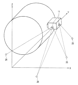
Here, a principle of position e~etection. wil:~. '~e
briefly described. This embodiment employs a
trilateration method that is similar to the position
detection means widely known as the GPS (Global
Positioning system).
As FIG. 5 shows, it is assumed that coordinates of
known three points (three fixed cc unication means in
this embodiment) B1, X32 and B3 are (x1, y1, z1), (x2,
y2, z2) and (x3, y3g z3) respectively, and a. coordinate
r
CA 02453960 2004-O1-30
_ ~°7
_ ~X~~X~ 2+ {.jP-Z-TT~ 2'~' ~, X-Z'°~~ 2
D~staz~ce ~rosn A ~o B~
~.~?=~X2'°X~ 2+ CY2~Y'~ 2+ ~ 22°Z~ 2
~3.~taFl~O ~rOIl1 ~ ''~o ~~ m
~..3=~I ~X.3'°X~ 2+ ~3~~.'3y~ 2+ (.~.3-2
y. CA 02453960 2004-O1-30
_ 2 g ...
receiving point by an equivalent of 2 ns. In the case
of this example the phase deviates by approximately 40
degrees. Thus~ based on such a relationship, the
distance between. the two can be acquired by checking an
amount of deviation of the phase from the predeterncined
phase on receipt at the receiving point (electric wave
receiving portion of the solid semiconductor element)
of the electric wave transr~citted fi:om tllae transmitting
point (fixed communication means) ~_n the predetermined
phase.
Moreover, in this embodiment, as the electric
waves from the three fixed communication means 26 are
received by one electric wave rece~..v~.ng portion, the
frequency, amplitude or pattern of the electric wave
transmitted from each of the fixed communication means
26 is changed respectively in order to identify each
electric wave . '.~'hLIS a each of the f L.xed communication
means 26 has an ~:.dentificata.on modulation function .~'~o
as to transmit an electr~.c ware uni~r~ue t.o it .
As above8 the position of the electric wave
receiving portion 16 of the solid semiconductor element
31 in the in7c jet recording apparatus 600 is
calculated. And then as a relative positional
relation between the sol.~.d seiconde~ctor eleynent 11 and
the ink discharge port in the ink jet recording headt
601 is required on manufacturing the ink jet recording
head 601, the position (actual discharge position) of
CA 02453960 2004-O1-30
29 -
the ink discharge port in the ink bet recording
apparatus 600 can be acquired.
Tn producing records by the ink ,bet recording
apparatus 600, one of the importani~ factors in
performing high-~prec~.sa.on and ~aigh--quality print~.ng is
instance. It is not easily feasibleA however, to
mechanically correct this ~.ev:iation~. of i:he relative
positions because it requires h~.ghly urge-scale work.
Thus, it is thin~~able to correct the deviation of tare
~5 record medium and the ink discharge pos~_t~.on by
shifting the timing of discharging the ink so as t~
perform high-precision and hig~a.-quality printing.
Accordingly, the actual ink discharge position is
acquired by the above described method, and then the
20 deviation from a desired position is checked, and
besides, the discharge timing control signal for
correcting the discharge timing as required for
correcting the deviation is transmitted from the
discharge timing control portion 19.
25 The above are the rna~or workings of the solid
semiconductor element 17. of this embodiment, and the
data required fog various calculation and so on are
CA 02453960 2004-O1-30
_ 30
stored in the memory 20 in advance. Under normal
conditions~ suc~a data as stored as initial data in the
memory 20 on manufacturing of the i.nk jet recordi~ag
head 601 or on manufacturing of the ink jet recording
apparatus 600.
Under normal conditions, the ink jet recording
head 609. has a driving signal supplied from the driving
signal supply means 24 of the recording apparatus body
2~ and discharges the ink selectiv~:ly in
synchronization with the movement of the carriage 607
so as to record a. desired ~.mage and so on~ In this
embodiment, however, the timing of ink discharge
instructed by the driving signal is. corrected by the
discharge timing control signal transmitted from the
discharge timing control portion 19 of f:he solid
semiconductor element ~.2 so as to discharge the ink.
Nevertheless, the discharge timing control. portion 19
does not transmit the discharge timLr~g control signal
in the case where the position detect~.o~: portion 1~ has
detected that the actual discharge ;position coincides
with the desired pOSitiOn.
Here, an overtriew of operation of the ink jet
recording apparatus of this embodiment will be
described by referring to the flowcharts of FIG. 6~ and
FIG. 6U. FIG. 6~ shows a manufacturing process of the
head, and FIG. 6~ shows use of the ink j,et recording
apparatus.
~ CA 02453960 2004-O1-30
..
The ink jest recording apparatus 6t90 of this
embodiment uses an unillustrated ~~.g in the
manufacturing p~:ocess of the head to actually measure
and acquire the relative posit.iona~. relation between
the electric wave receiving portion 16 of the solid
semiconductor element 11 in the in:k jet recording head
601 and the ink discharge ports And the measured data
is stored as in~.t~.al state data in the memcary 20. And
various data. is stored in the memory 20 of the solid
semiconductor element 11, such as how t~ adjust the
discharge timing t~ correct such a positional relation
when it deviates from the ~.n$ta.al state, that a.s, when
~'a'llCih a p~S°l.t~onal relatl.on a.s not GA des:lred one, s'3.nd
the equations required fox calculation for the sake of
position detection of the solid semiconductor element
11 as described abovem
Thereaf ter ~ when the ~.nk jet recording apparatws
600 is completed and used by a user~r first, the time
signal is transmitted from the time signal transmission
portion 25 to the solid semiconductor e~.ement 1~., and
the time signal receiving portion 21 receives it and
then determines whether the time of the t~.me signal
coincides with that of the clock 22,. and in the case
they do not coincide, it corrects the clock 22 to
coincide therewith. And electric waves for position
detection are transmitted from the three fi.~ed
communication means 26 to the solid semiconductor
CA 02453960 2004-O1-30
_ 3'~1
element 11. The electric wave receiving portion lfi
receives them, and the electric wave analysing portion
17 and the position detection portion 18 calculate the
respective distances from the fixed communication means
26 to the electric wave receiving portion 16 based on
the phase deviations as aforementioned so as to acquire
the position of the electric wave receiving portion 16
in the ink jet recording apparatus 6~0 based thereon
and acquire the position (actual discharge position) of
the ink discharges port in the ink jet recording
apparatus 6~~ based thereono In th.e case where the
position of the ~3ischarge port thus acquired is
different from the initial state, the discharge timing
is shifted in this embodiment in order to make up for
.L5 this deviation. And then, the discharge timing control
portion 19 transmits the discharge timing control
signal to the liquid discharge portion ~3. lHoreover,
all the various data and so on requ.tred for the above
data. processing are stored in the memory 20 in advance.
2;0 In addition, it is desirable to store tyre deviation
thus detected in the recording mean:.
The liquid discharge portion 2:~ as controlled by
the driving signal supplied by the c"l.riving signal
supply means 24 of the recording apparatus body ~8 and
~5 the discharge timing control signal from the discharge
timing control portion 19, and produces :records by
ejecting ink droplets onto the printing paper P in
CA 02453960 2004-O1-30
~ ~~
synchronization wath feeding of the printing paper P
and reciprocating movement of the carriage 607.
Moreover, the solid semiconductor element 11 is
operated by the electromotive force supply means 622
supplying electromotive force l2 to the solid
semiconductor element 11, and the energy converting
means 14 converting the electromotive force 12 into the
power 13 and then activating the discharge control
means 15 by that power.
It is also possible to have a configuration
wherein a galurality of the solid semiconductor elements
are provided in recording head. This is because
providing only one solid semiconductor element may
create a dead angle of communication cons~.dering that
the carriage moves irs an extended range, surrounded by
various other members and also that records will be
produced on a three-dimensional object ~.n the future.
In addition, in the case of providing a plurality of
the solid semiconductor elements as described above,, it
2~ is desirable to provide four or more of the fixed
communication means 26 on the recording apparatus body
as shown in FIG. 7. Thus, it is possible to malts
discharge position detection high-precision by
providing two or more of the solid semiconductor
element 11 and providing four or more of the fisted
communication mee.ns 2~.
In the case.of providing a plurality of the solid
CA 02453960 2004-O1-30
_ 3 a~ ..,
semiconductor elements, while independent elements as
shown in FIG. 4 can be separately prepared, it is also
feasible to ren~.er certain functions in common so that
the solid semiconductor elements can communicate with
one another.
According to this embodiment, as the solid
semiconductor element 11 has the energy converting
means 14, it is no longer neoessa.r~r to ;implement direct
electrical wiring with the outside, and it is possible
to use the solid semiconductor element 11 even at
locations where direct electrical cwiri.ng with the
outside is difficult so that the position of the
discharge port c~.n be grasped in real time during the
movement of the ?carriage 6~b7. In addition, as the
solid semiconductor element 11 has the energy
converting means 14, it is no longer nec;essary to p:Lace
means for accumulating the electromotive force for
operating the solid semiconductor element 17., and sa it
is possible to render the solid semiconductor element
~0 11 smaller so that it can be placed even in a narrow
location.
Moreover, as a two-way communication method
between the solid semiconductor element and the
outside, it is possible to apply a r_°adl.o LAN system
using a microwave bind frequency or a radio access
system utilizing a quasi-millimeter wave/millimeter
wave frequency.
CA 02453960 2004-O1-30
- 35 -
Here, an o~rerview of sending and receiving by the
radio LAT1 systex~l will be described. ~Yae following will
describe data transmission from the solid semiconductor
element to the recording apparatus. moreover, in the
case of inversely performing data transmission from the
recording appar~.tus to the solid. semiconductor element,
a data ID is pl~.ced on each side so that they can be
identified thereby.
the solid semiconductor element on the
Im transmitting side has a line monitoring portion, a data
handling portion, an acknowledgement check portion and
an error processing portioxx, and t~xe ree:ording
apparatl'IS on thE'. . recel.vJLng side hail a C~i~t~ handling
portion, an acknowledgement portior~~ an error
processing port~.on, a display portion axed so on placed.
FIG. ~ show: a flowchart ~.n the so,~_id
semiconductor element on the transmitting s,ade. In the
case of transm~.tting data, init:~ali~ation is performed
by a determined transm~.ssion protocols and then an
~0 address on the r~;ceiving side is set anc~. data is
transmitted. In the case where signals collide during
the transmission or no acknowledgement is returned from
a specified apparatus on the receiving side~ it is
resent. 'G~hile in operations it displays a state of the
line and whether or not there is an acknowledgement on
a display portion ple.ced on the recording apparatus on
the receiving side so as to prompt the user to make an
CA 02453960 2004-O1-30
36
accurate determ~.nat.fon.
FIG. 9 shows a flowchart in the recording
apparatus on the receiving side. tin this receiving
side, it constantly monitors the line, and if its own
address is confirmede it takes in the data from the
line and accumulates it in a buffer on .a main memory.
In the case where a block mark per 1~ bytes cannot be
confirmed during receiving or a check sum does not
match in an error detection process after completion of
receiving, it interrupts receiving as a receiving
error, monitors the line again.~ and waits for arrival
of the header. 3n the case of receiving it without an
errors it displays the received c~ntents on the display
portion.
The solid semiconductor element 11 can have
various functions in addition to a series of the above
described operat~.on of discharge position detection and
discharge timing control.
Second embodiments
~0 Next, a c~an3aiguration where~.n the >>olid
semiconductor element is used for a configuration for
detecting the st~.te of the ink tank will. be described.
FIG. 10 shows a block diagram showing internal
configuration of the solid semiconductors element 11
~5 axsed for the ink jet recording apparatus of a second
embodiment of the present i~wention and its exchanges
with the outside. As shown in FIG. ~, the ink jet
CA 02453960 2004-O1-30
~ ~ 'y.
recording apparatus 500 has the standstill
electromotive force supply means 6~2 for supplying
electromotive force that is external energy to the
solid semiconductor element 11 and the movement time
electromotive force supply means 6~~ as well as means
for perforaning two-way communication of information
with the solid semiconductor ~5.~:memt 11 (unillustrated)
installed therein. As mentioned later, the
electromotive force supply means 6~2 and. 623 generate
the electromotive force for operating the solid
semis~nductor element 11 bar the electromagnetic
induction.
this solid semiconductor element 1:t has an energy
converting means 114 for converting into power ~.1~
electromotive force 112 supplied from an outside ~
(electromotive force supply means 6~~ or 523) to the
Solid SemicOnduc'Or elePlient 11 in a nonwcOntaCt manner
and an information acquiring means 115 activated by the
power acquired by the energy converting means 114~ and
?.0 a discriminating means 316 an info ati.on storing
means 11°7 and a~a information communicating means 11th,
and is placed in the ink tank mentioned later. °~he
electromotive force supplied to operate the solid
semiconductor el~:ment 11 is generated 'by the
electromagnetic induction. It is desirable that at
least the energy converting meaa~s 11~ and the
information acquirir3g means 115 should be formed oz~ or
CA 02453960 2004-O1-30
~ ~~ w<
near the surface of the solid semiconductor element 11.
The information acquiring means 115 acquires
information in the ink tank, which is environmental
information of the solid semicondu~~tor element 11. The
discriminating rr~eans 116 compares 'the in-tank
information acquired from the information acquiring
means 115 with information stored in the informat~.cm
storing means 117 and determines whether or not the
acquired in-tank information should be transmitted to
the outside. The information storing means 11~ stores
the in-tank information acquired fx,om tine information
acquiring means 115 and the conditions 'to be compared
with this in-tank information. The: information
communicating means 11~ corwerts the power into the
energy for transmitting the in-tank information
according to an order of the discriminating means 116
so as to display and transmit the in°~tank information
to an outside ~.
FIG. 11 is a flowchart for explaining operation of
a~ the solid semiconductor element 13 shown in FIG. 1~.
As shown in FIG. 1~ and FIG. 11, if the electromotive
force 112 is given from an outside .~ electromotive
force supply mearjs) to the solid semiconductor element
11, the energy converting means 11~ converts the
electromotive force 11~ into the power 113, and
activates by that power the information acquiring means
115, the discriminating means 116, i=he information
r . CA 02453960 2004-O1-30
3g
storing means 1~.7 and the information communicating
means 118~
The activated information acquiring means 115
acquires information in the ink tank, which is
environmental information around the solid
semiconductor element, such as an ink residual amount,
are ink type, temperature and pH (step S11 in FIG. 1I).
Next, the discriminating means 7.16 reads from the
information storing means x.27 cond3.tions for referring
1~ the acquired in-tank information to (step S12 in FIG.
12), and compares the read. conditions with the acquired
in-tank information to determine necessity of
transmitting the information (step S13 in FIG. ~.1).
Here, the condit_~.ons preset in the ~nformat:~.on storing
means 117 are a minimum residual amount of the ink (2
ml for instance)k. pH of the ink and so on for instance,
and it is determined based thereon Lhat, when the
residual amount of the ink becomes ~ ml or less or pH
of the ink great~.y changes, it is necessary to transmit
2~ necessity of tank replacement to the outside.
In the case where the discriminating means 116
determines that it is not necessary to transmit the in-
tank information to the outside in step 513, the
current in-tank information is stored in the
information storing means 117 (step S14 in FIG. I1).
This stored information care also be compared uaith the
information acquired next by the ~.nforma~ti.on acquiring
CA 02453960 2004-O1-30
means 215 by the discriminating means 136.
I~loreover, in the case where the discriminating
means 11~ determines that it is necessary to transmit
the in-tank information to the outside in a step X13,
the power acqui~:ed by energy conversion is converted by
the information communicating means 118 into the energy
for transmitting the in-tank information to the
outside. This energy for transmitting is capable of
using magnetic fields, light, shape, ccolor, electric
waves, sound and so on, and for instance, in the case
where it is determined that the in:Ic residual amount has
become 2 ml or less, it transmits ,~.ecessity of tank.
replacement to the outside B (such as the ink jet
recording apparatus] by sounding (step S15 in FIG. 11}.
In addition, the target of transmission is not limited
to the ink jet recording apparatus body but it can also
be transmitted to the human sense of sight or hearing
especially in the case of light, shape, color, sound
and so on. Furthermore, the transmitting method can be
changed according to information, for instance,
transmitting it by sound in the case where it is
determined that the ink residual an;~ount has become 2 ml
or less, and by light in the case where pH of the ink
has greatly changed.
In the case of being used for the ink jet
recording apparatus, the standstill. electromotive force
supply means 622 for supplying electromotive force as
CA 02453960 2004-O1-30
- 41 -
external energy to the solid semiconductor element 21
should be placed at the home posit.lon so that the
carriage 607 will certainly visit it between completion
of printing and start of printing of a magnetic field,
and consequently there is little possibility that the
electromotive force supply to the solid semiconductor
element is delayed. In addition, it is possible to
know the internal state of the ink tank by using the
electromotive force supply means, which can be used for
inspection (quality assurance) if used by a factory or
a distributor. The electromotive :E~orce supply means
and method will be mentioned later.
This embodiment has the above-mec~tioned solid
semiconductor elements accommodated in the ink tank.
FIG. 12 to FIG. 15 show examples of configuration of
this ink tank. As for an ink tank 501 shown in FIG.
I2, it has a flexible ink bag 502 placed in a housing
503, a bag mouth 502a closed with a rubber plug 504
fixed on the housing 503, and a hollow needle 505 for
leading the ink stuck into the rubber plug 504 and
pierced through the inside of the fag so as to supply
the ink to the u~°~illustrated ink jet head. A solid
semiconductor element 506 can be placed in the ink bag
502 of such an ink tank 502.
In addition, an ink tank 511 shown in FIG. 13 has
an ink supply port 5I4 of the housing 51.2 accommodating
ink 513 on which an ink jet head 515 for discharging
CA 02453960 2004-O1-30
42 -
the ink onto re~:ording paper S for' recording is
mounted. A solid semiconductor element 516 of the
present invention can be placed in the ink 513 in such
a tank 511.
I~ioreover, an ink tank 521 shown in FIG. 14 is a
tank similar to the one shown in t:he embodiment
described later and it has a first chaimber in a
completely sealed state for accommodating ink 522, a
second chamber in a ventilating state for accommodating
a negative pressure generating member 523~ and a
communicating p~.th 524 for co unicating the first
chamber with the second chamber at the tank bottom.. If
the ink is consa~aned from an ink supply port 525 on the
second chamber side, the air flows from the second
15, chamber into the first chamber, and instead, the ink
522 of the first chamber is led out to the second
chamber. It is also feasible, in t:he tank 522 of such
a configuration, to place solid semiconductor elements
525 and 526 in the first chamber and the second chamber
respectively so .as to exchange information on the ink
in each of the divided chambers.
In addition, an ink tank 531 shown in FIG. 15 has
an ink jet head 533 mounted, which accommodates a
porous member 53'Z holding the ink and uses the
accommodated ink for recording. The tank 531 of such a
configuration can also have solid semiconductor
elements 534 and 535 placed on the ink tank side and on
CA 02453960 2004-O1-30
_ 4~
ink jet head side respectively to exchange information
on the ink in the respective divided components as with
the tank shown in the embodiment described later.
According to this embodiment, as the solid
semiconductor elements have the energy converting
means, it is no longer necessary to implement direct
electrical wiring with the outside, ana'~. so it is
possible to use the solid semiconductor' elements in any
location in the object, that is, e,~ren at locations
1~ where direct electrical wiring with the outside is
difficult or in the ink as shown in FIG. 12 to fIG. 15
as described above. It becomes possible, by placing
the solid semiconductor elements in the ink, to grasp
the state of the ink correctly in real time.
In addition, as the solid semicondwctor elements
have the energy converting means, it is no longer
necessary to place means (a power supply in this
embodiment) for accumulating the electromotive force
for operating the solid semiconductor elements, and so
2a it is possible to render the solid semiconductor
elements smaller so that they can be used in any
location in the object, that is, even in a narrow
location or in the ink as shown in ~3G. 4 to fIG. '7.
Next, preferable concrete examples in the case of
~5 placing the solid semiconductor elements of this
embodiment in the ink tank will be described further in
detail.
CA 02453960 2004-O1-30
4~ -
First, the information acquirvng means applicable
to the solid semiconductor elements of this embodiment
are taken as examples. In the case where solid
semiconductor e:~ements to be placed in the ink tank are
created into spherical silicon, the fo~_lowing can be
named as the above described information acquiring
means. (1) A sensor for creating an Si~Z film or an SiN
film as an ion-sensitive film to detect: pH of the ink.
(2) A pressure sensor having a diaphragm configuration
1C~ for detecting pressure change in t:he t~.nk. ( 3 ) A
sensor for converting light into t:herma.l energy,
creating photodz.odes having pyroelectric effects,
detecting a current position and detecting an ink
residua. amount. (4) ,~ sensor for detecting whether or
not there is ink from an in-tank water amount by
utilizing the electrical conductivity of materials, and
so on.
Next, the energy generating means applicable t;o
the solid semiconductor elements of the present
invention will be described. FIG. ~~ is a diagram for
explaining power generation principle of the energy
generating means that is a componerdt of the solid
semiconductor element of the preser.~t invention.
First, this power generation principle will be
:25 described by referring to F'IG. 16.
In this embodiment, a coil (an inductor) is
provided to the solid semiconductor' elennent so that the
CA 02453960 2004-O1-30
...
electromotive force supply means changes a magnetic
flux around the coil so as to generate induced
electromotive force to the coil by electromagnetic
induction. To be more specific, if an electric
conductor coil L of an oscillation circuit 102 is
placed next to a coil La of an external. resonance
circuit 10I of the electromotive force supply means,
and a current Ia is fed through the coil La through the
external resonance circuit 101, a magnetic flux
piercing through the coil L of the oscillation circuit
102 is generated: by the current Ia. Here, if the
current Ia is changed, the magnetic flux H piercing
through the coil L changes so that induced
electromotive force Zl occurs to the coil L.
Accordingly, the oscillation ci~°cu.-'~t 102 as the energy
generating means is created in the spherical silicon,
and the external resonance circuit 101 as the
electromotive force supply means is placed on the ink
jet recording apparatus outside the solid semiconductor
element in such a way as to have the electric conductor
coil L of the oscillation circuit 3.02 on the solid
semiconductor element side placed next to the coil La
of the external resonance circuit 101 outside the solid
semiconductor element, so that the power for operating
the solid semiconductor element is generated by the
induced electromotive force due to the electromagnetic
induction from the outside.
CA 02453960 2004-O1-30
- 46 -
In addition, as the magnetic flue B piercing
through the coil L of the number of tuaws N of the
oscillation circuit 1(~2, which is created in the
spherical silicon as the energy generating means will
be as follows assuming a proportionality constant is k,
since it is proportionate to the product of the number
of turns Na of the coil ~a of the eternal resonance
circuit 1~1 and the current Ia.
B = k x Na x Ia (1~
1~ The electromoti~re force V occurring to the coil h
will be as follows.
V = N{dB/dt}
.- -kNaN{~.Ia/dt~
- -1K{dla,'dt~
35 Here, if permeability of a magnetic core of the
coil as ~aa and the magnetic: field _Ls Vii, the magnetic
flue B will be as follows.
B = paH(z)
{ ~aNd~a~';~z/ 2 ( rat + Zl ) 3~2 ( 3
2~ Here, z indicates the distance between the coil of
the external resonance circuit and. the coil create. in
the spherical silicon.
The mutual inductance of the eguation: 1~I will be
as follows~
25 I~ _ {~N/'liala} f SB ~ d~
- { pha~'a2N~NS/ 2gy ( ~°$2 -~° ~z ~ s/z } ( ,4 ~
Here, uQ is space permeability.
CA 02453960 2004-O1-30
4'~
And the impedance of the oscillation circuit
created in the spherical silicon: Z will be as follows.
Z ( cu ) - R + j ~ cc~L - ( 1 /r~C ) ~ ( 5
The impedance of the external resonance circuit:
Za will be as follows.
Za(t~) - Ra + jc~La - ~w2Ma/Z(t~);~ (6)
Here, J represents magnetization. And the
impedance on resonance (when current value: Ia becomes
maximum) of the external resonance circuit: Zo will be
1~ as follows.
Zo(wo) - Ra + jLac~o - ( ~2MZ/R) (7)
The delay of the phase of the external resonance
circuit: ~ will be as follows.
tank _ ~ jLawo - (cz~Q2M2/R) }/R
And the resonance frequency of the external
resonance circuit: fo will be as follows.
f0 = 1,12~c(LC)1~2 (9)
Due to the above relationship~ if the impedance of
the oscillation circuit 102 created in t:he spherical
~~ silicon varies according to the change of the ink in
the ink tank, it changes the frequency of the external
resonance circuit 101 so that the above change of the
ink shows in the amplitude and the phase. difference of
the impedance of the external resonance circuit IOW.
In addition, the phase difference and amplitude include
the ink residual amount (that is, change of z).
For instance, as making the resonance frequency of
CA 02453960 2004-O1-30
- 4~
the external resonance circuit 10~.. var=Lable changes
output (impedance) from the oscillation circuit 102
created in the spherical silicon according to
environmental change, ~t ~s possible, by detecting this
frequency dependence to detect whether or not there is
ink and the ink residual amount.
Accordingly, it is possible to use the oscillation
circuit 302 created in the spherical silicon not only
as the energy generating means for generating power but
also as part of means for detecting the change of the
ink zn the tank in the relat~.onship between the
oscillation circ>uit 102 and the external resonance
c~.rcuit 101.
Based on such a principle, the concrete means and
1~ method for supplying the electromotive force to the
solid semiconductor element will. be described by
referring to FIG. 17 to FIG. 24. Moreover, in order to
make them easier to understand, FIGS. 17, 18, 20 and 23
only ,show the ink tank, leaving out the carriage and
the recording head.
As shown ~.n FIG. 17, an ink tank X41 mounted on
the carr~.age 607 reciprocates during printing and
recording, and stops at the home position HP provided
outside the recording area while not pr.~.nting. tahile
not printing, at the home position HP, the head
cartridge 601 shown in FIG. 3 has t:he suction recovery
process and so on performed. by the cap member 614, the
CA 02453960 2004-O1-30
- 49 -
ink absorbing means 63.5 and the cleaning blade 6~7. In
this embodiment, the electromotive force is supplied to
the solid semiconductor element 11 wl~.i~.e the carriage
607 is at standstill at the home position ~iP.
In order to generate the induced electromotive
force on the so~.id sem~.conductor element 11 by
electromagnetic induction in compliance with the above
described principle' an electromagnetic apparatus 622
is placed as the standstill electromotz.ve force supply
means at the home position HIS. The electromagnetic
apparatus 622 is roughly U-shaped, where both ends 622a
and 622b are placed oppositely sandw~.ching a carrier
path (range of movements 625 of the carriage 607. And
when the electromagnetic apparatus 622 is in operation,
both the ends 622a and 622b become magnetic polesa that
is, either an ~ pole or an N pole, and generate the
magnetic flux pa.ercing through the solid semiconductor
element 11 in the ink tank 541 mounted on the carriage
607~
In this embodiment, as the electromagnetic
apparatus 622 is AC-driven and magnetic properties of
both the ends 622a and 622b contimxe to change
mutually, as shown in ~'IG. 1~, the magnetic flux B
piercing through the solid semiconductor element 12
continues to change constantly. To be more specific,
as the magnetic flux B piercing through the coil L
shown in fIG. 16 changes, the AC-induced electromotive
CA 02453960 2004-O1-30
..
s~xpp~~.ed t~ ar~~ ~~t~i~r~tes the ~n~c~.r~~t~~n ~cquiria~g
CA 02453960 2004-O1-30
_ 6z _
plurality of pez~manent magnets on the carrier path
(range of movement) 626 of the car~°iage 607 as shown in
FIG. 2~. Accor~3ing to this configuration, if the
carriage 607 reciprocates during printing operation,
6 the coil L of t~~e solid semiconductor element 11.
crosses inside the magnetic flux B due to permanent
magnets 623 as :shown in FrG. 23., a:nd so AC-induced
electromotive force is generated on the coil L. And as
described above, the AC-induced electromotive force is
1o rectified and rE:ndered smooth. and stable to be used for
activating and operating the means of the solid
semiconductor element and also accumulated in the
unillustrated betttery and capacito:G (see FIG. 22).
According to this configuration, it is possible to
16 constitute the r~'ovement time elect_~omotive force supply
means with perm~:nent magnets 623 so as to generate the
electromotive force by electromagnetic induction,
utilizing the movement of the carriage 6~7.
Accordingly, the power can be acquired either while the
2~ carriage 6~7 is at standstill at tk~e ho:~ne position HP
or while it is rr~oving for printing operation and so on~
so that activation and operation of the solid
semiconductor element 3.1. becomes highly stabilized with
no possibility of power shortage.
26 PZoreover, as shown in FIG. 23,. ifboth magnetic
poles of the permanent magnets 6~3 are placed
oppositely sandwiching a carrier path (xange of
CA 02453960 2004-O1-30
52 --
movement) 625 of the carriage 607, the magnetic fl~,xx l3
piercing throug:~a the coil is of the solid semiconductor
element 11 can be formed so that greater effects of the
electromagnetic induction can be acquired. In
addition, the electromagnetic apparatus can be used
instead of the permanent magnets. In this case, it is
not necessary tc~ constantly change the magnetic flux by
A~-driving unliltbe the electromagnetic apparatus 622
planed at the home position HP.
Here, the ink jet recording apparatus of this
embodiment will be described by referring to the
flowchart in F1~~. 24.
If the power of the ink jet recording apparatus is
energized (S101), it is first ch.ecl~.ed whether the
carriage 607 is at the home position HP by the
photocouplers 6i1 and 612 (see FIG. 3) (5102). In the
case where the carriage 607 is not at the home position
HP, the drive motor 602 as operated so as to move the
carriage 607 to the home position HP (51.03)a
At the home position HP, it i:~ checked whether
sufficient power is accumulated in the solid
semiconductor element 11 ire an ink yank 700 of the
carriage 607. ~"o be more specific, ~. signal is
transmitted by t:he communication means of the .ink jet
recording apparatus body to the sol.~.d semiconductor
element 11 (5104). If the solid sem~.conductor element
11 is in an operable state, it responds after receiving
CA 02453960 2004-O1-30
- 5~
the signal (S1~!i)o As opposed to this, in the case
where there is aio response from the so3.id semiconductor
element 11 to the communication means of the ink jet
recording apparatus body, it is determined that
sufficient power is not accumulated in the solid
semiconductor e~.ement 11 and it is inoperative, so that
the electromotive force is supplied thereto (SlU6). To
be more specific;, as described above, the
electromagnetic apparatus f22 positioned at the home
1~ position HP is ~C-driven so that the electromotive
force is generated to the solid se~rsiconduetor element
11 by the electromagnetic induction.
Next, a signal is transmitted ~y the communication
means of the ink: jet recording apparatus body to
operate the solid semiconductor elennent 11, and the ink
residual amount in the ink tank 54:L is detected based
on the above described equation (S:L~~7) to determine
whether or not there is ink (Sl~D8). In the case where
it is determined that there a.s no ink or only
insufficient ink, an instruction of the ink tank
replacement is displayed (S109). ~n the case where. it
is determined that there is suffic~_ent ink~ as
described above, records are produced by ejecting ink
droplets from the liquid discharge head onto the
printing paper P in synchron~.~atiora with feeding of the
printing paper P and reciprocating ~saovement of the
carriage 647 (5110 . if the printing is completed, the
CA 02453960 2004-O1-30
54
entire operata.c~c~ is terminated.
Next, how to manufacture the solid semic~nductor
element of this embodiment 11 will be described. FIGS.
25A to 25G is a process drawing for explaining an
example of the ~nanufactur~.ng method of the solid
semiaonducte~r element of the present invention, where
each of the prcresses is shown as s. section passing
through the center of the spherical sil.icon~ ~d~reover~
a manufacturing method is exemplified here, whereby the
center of gravity of the spherical silicon is made
lower than the center, and the upper part inside the
sphere is made ~iollow and the holl~~w pa~rtion is kept
airtight.
After forrn~_ng a thermally ~sxi~~i~ed. Si02 film 202 ~n
the entire surface of the spherical silicon in FIG.. 25A
as shown in FIG. 25B, patterning is performed by using
a photalithograg~hy process, ans. an opening 203 is
formed in part cf th.e Si02 film as shown in FIG. 25C.
And as sho~a~n in FIG. 251D, the ~xpper part of the
silicon is partially removed by aniso~t.rapic etching
using KOH solution through the ~pening 203 to form a
hollow portion 204. Thereafter, as shown in FIG. 25E,
an ~PCVD method is used to form an SiN film 205 on
inner and ~uter surfaces of the so7_ld semiconductor
element.
Furthermore, as shown in FIG. ~5F~ a metal C'4~
method is used to form a Cu film 20~a on the ent~.re
CA 02453960 2004-O1-30
surface of the solid semiconductor element. And as
shown in F"IG. 25G, patterning is performed to the Cu
film 206 by using a known photolithography process, and
the electric conductor coil L of the number of turns N
that is a part of the oscillation circuit is formed.
Thereafter, the solid semiconductor element comprising
the electric conductor coil L is taken out of a vacuum
device into the air, and the upper opening 203 is
blocked by a sealing member 20"7 that is a resin, a plug
or the like so as to render the ho3..low portion 204 in
the sphere airtight. If manufactured in this manner,
1t allows the S~)lid SemiCOnduCt63r element cOmpriSed Of
silicon itself to have buoyancy without: having means
for generating buoyancy by using power as in a third
embodiment mentioned later.
In addition, IV-M~S circuit el~ea~ents are used ~=or
driving circuit elements other tha:ra the coil L to be
formed in the spherical silicon before manufacturing
such floating-type solid semiconductor elements. fIG.
18 shows a schematic section view wherein an N-M~~
circuit element is vertically cut.
According to SIG. 26, on an Si substrate 401 of a
P electric conductor, ~-Mos 450 is constituted in cin -
type well area 402 and N-Mos 451 is~ constituted in a P-
type well area 403 by impurity introduction and
diffusion such as an ion plantation using a general Mos
process. The P-Mos 450 and N-Mos 451 a.re comprised of
CA 02453960 2004-O1-30
~ 56 -
gate wiring 415 by poly-Si deposit:ed to thickness of
4,000 angstroms to 5,000 angstroms by ithe CVD method
via a gate insulating film 408 of several-hundred-
angstrom thickness respect.~vel~°, a.nd a source area 405,
a drain area 40~ and so on to which N-type or P-type
impurity introduction has been performed, and C-Mo,s
logic is comprised of such P-Mos 450 and N-Mos 451.
An N-Mos transistor 301 for driving elements as
also comprised of a drain area 411, a source area 412
and gate wiring 413 a.nd so on on the P-type well
substrate 402 by the processes such as impurity
introduction and diffusion.
Here ~ if the T3-Mos transistor 305. is used as an
element-driving driver, a distance h between the drain
25 gates comprising one transistor becomes approximately
10 pm as ~. minir~~um value . A part s~f a breakdown of: the
10 pm is width of contact 417 of the source and thE.
drain that is 2x2um, whereas it is actually 2 ~a that
is 1/2 thereof since a half thereof is shared with an
adjacent transistor. The rest of i~he breakdown is
comprised of a distance between the contact 417 and the
gate 413 that is 4 um of 2x2 , and width of the gate
413 that is 4 um, so that the total. is 10 dam.
,Among the elements, an oxide ~ilm separating area
453 is formed by field oxidation of thickness of 5,000
angstroms to 10,000 angstroms for element separation.
This field oxide film acts as a first thermal storage
CA 02453960 2004-O1-30
- 57 -
layer 414.
After the a~lements are formed, an interlayer
insulating film 416 is deposited with f~SG and ~PS~
films and so on to be approximately 7,Ci0t~ angstroms
thick by the CVD method and flattened. by heat
treatment, and :hen wiring is performed by an AT
electrode 417 to be a first wiring layer via a contact
hole. Thereafter, an interlayer insulating film 418
that is the Si~2 film by a plasma method is
1~ deposited to be 1~,d0a angstroms to 15,~C~~ angstroms
thick and a through hole is further for~nned.
This N-Mos circuit is formed before forming the
floating-type solid semiconductor element as in FIGS.
25A to 25G. Any' connections are m~.de to the
1~ oscillation circuit as the energy generating means and
the sensor portion as the information acquiring means
and so on of flee present invention via the above
through hole.
In addition, whatever state the in:k tank on which
20 the floating-type soled semiconductor e.l.ement of tb.is
embodiment is placed is in, a stable magnetic flux
(magnetic field) must be working between the
oscillation circuit created in the spherical silicon by
the above-mentioned manufacturing method and the
25 external resonance circuit shown in ~'IG. 16. In the
case of floating in liquid such as the ink, however, a
liquid level may oscillate due to external oscillation.
CA 02453960 2004-O1-30
- 5~
Even in Such a ~.~.aS~, the center Of gravity of the
floating-type salad semiconductor element is determined
in this embodiment in order to maintain a stable state
in the liquid.
As shown in FIGS. 27A and 278, in the case of
floating a solid semiconductor element 210 of this
embodiment in the liquid, the following relationship
must hold in order to be in a balar°$ced state as shown
in FIG. 27A°
(1) Buoyancy F = object weight W; and
(2) The lirae of action of buoyancy and the line of
action of weight (a line passing through the center of
gravity G) coincide.
Reference character S indicat'rs an ink level.
And as in fIG. 278, when the liquid is oscillated
by external force and the solid semiconductor element
210 inclines a little from the balanced state, the
center of buoyancy moves so that the buoyancy and the
weight make a couple of forces.
2o Mere, the point of intersection of the line of
action of weight in the balanced state (a dashed line
in FIG. 27B) and the line of action of buoyancy when
inclined (a solid line in FIG. 27B) is referred to as a
mete center ~C, and a distance h be:~:ween the mete
center and the center of gravity is. referred to as
height of the mete center.
As shown in this embodiment, the mete center of
CA 02453960 2004-O1-30
the solid semiconductor element 21.0 is at a higher
position than t~.-ae center of gravity~ and so the couple
of forces (restoring force) works in a direction to
return to the o;~~.ginal balanced position. This
restoring force: T will be as follows.
T = iahsin~ ~ Fhsin~
.- pgVhsin~ ~>0)
Mere ~ volume of the l~.quid el~.znin~~ted by the solid
semiconductor e~.ement X10 is 5~, and specific weight of
the solid semicr~nductor element 210 is pg.
Thus , in ox:der to make this resto~°ing force
positive, it is a necessary s.nd suffica.ent condition to
be h>0.
And it wine be as follows from fIf-a 27H.
h= (1/V~ --CG
Here, I is moment of inertia about an axis O.
Accordingly, it will be as follows.
C ~% v~ > CG
The above is a necessary condition for the solid
semiconductor element CIO to float stably in the ink,
supply the induced electromotive force :From the
external resonan:e circuit and perf orm 'two-way
communication with the communication means outside the
solid sem.aconductor element.
CA 02453960 2004-O1-30
m 6~
As for a method of the two-way communication with
the external communication means, sending and receiving
and so on in this case, as aforementioned, it is a
configuration wherein it is possib~~e to apply the radio
7LAN system using a microwave band frequency or the
radio access system utilizing a quasi-nnillimeter
w~.vC'r~'ml~.~lmete~' wave ~requenC3y a and the Solid
semiconductor element on the transmitting side has the
l~.ne monitoring portion, the data handling portion, the
1~ acknowledgement check portion and the error processing
portion, and the: recording apparatus on the receiving
side has the data handling portion, the acknowledgement
portion, the er~°or processing port.~on, the display
portion and so on placedo A flowchart in the solid
15 semiconductor element on the transmitting side is as
shown in FIG. ~, and a flowchart in the recording
apparatus on the receiving side 3s as shown in FIG. 9~
In addition, the solid semiconductor element of
the present invention is preferably applied to an ink
2o jet printer wherein the ink accommodated in the
removably pieced ink tank is supplied to the ink jet
recording head, and the ink information and the tank
information on t:~ae ink jet printer printed on the
recording paper with the ink droplets ejected from the
25 recording head i:, detected, and the. information is
transmitted to the ink jet printer to control the
printer by the most suitable method and control it for
CA 02453960 2004-O1-30
maintaining the optimum state in the tank.
Moreover, while the exterior of t~:~e ink bet
recording apparatus is unillustrated ~.~~ this
embodiment, it is possible, in the case of using an
exterior cover and also an ink tank that are
translucent or something similar capabae of showing the
inner state, to use light as the communication means so
that the user can see the light of the tan% and easily
understand that °the tank should be ~'eplaced" for
ZO instance, making the user desi.~°ous of z°eplacing the
tank. ~onvent~.onally, it was not easy for the user to
understand what message was being givexa even if a
button on the apparatus body l~.ghted up since at had
several display functions. F3owever, this embodiment
makes it very easy to understand the necessity of tank
replacement.
(~hlrd ~mbodimeot~
F°IG. 28 is a block diagram showing the internal
configuration of the solid semiconductor element of a
third embodiment and its ehchanges with the outside;.
Moreover, as th~.s embodiment is the same ~.s the f~.r~st
embodiment as to the constitution other than the solid
semiconductor element, such description is omitted.
fhe solid s~rmicond~actor element 21 shown in this
ciiagrem has an energy converting means :L24 for
converting into power 123 electromotive force 222
supplied from the outside A (electromotive force supply
CA 02453960 2004-O1-30
62 -
means 622 or 623 to the solid semiconductor element 21
in a non-contact manner, an ~.nform~.tio'a acquiring means
125 activated bvy the power acquire:r~ by the energ~~
converting mean 124, a discriminating means 126, an
information storing means 127, an information
communicating means 128 and a receiving means 129, and
is placed in the ink tank. It is ~.ifferent from the
second embodiment in that it has a receiving funct:~.on.
In addition, it is desirable that a.t least the energy
converting means 12~, the information acquiring means
125 and the receiving means 129 are formed on or near
the surface of the solid semiconductor element.
The information acquiring means 125 acquires the
information in the ink tank that i:~ envaronmental.
information of the solid semiconduwtor element 21. The
receiving means 129 receives an input signal 120 from
the communication means of the outside .A or the outside
B. The discriminating means 126 has the information
acquiring means 125 acquire the in--taa~k information.
according to the input signal from the receiving means
i29, and compares the acquired in-tan3~ information with
the .information stored in the information storing means
127 so as to determine whether or not the acquired in-
tank information meets predetermined conditions. The
information storing means 127 stores ~~arious conditions
to be compared w:'th the acquired inatank information
and the in-tank information acquired from the
CA 02453960 2004-O1-30
°'° ~ 3
information acguiring means 125. ~'he :i.nformation
communicating means 128 converts tb.e power into energy
for transmitting the in-t~.nk information according to
an order of the discriminating means 126 so as to
display and trav~.smit the results of determination by
the discriminating means 126 to the outside A, the
outside B or the outside C.
FIG. 29 is a flowchart for explaining operation of
the solid semiconductor element shown. 3_n FTG. 28.
Referring to FTC. 28 and FTG. 29, if e3_ectromotive
force 122 is given from the outside A (electromotive
force supply means) to the solid semiconductor element
21, the energy converting means 12~ coa?.verts the
electromotive force 122 into power 123, and activates
by that power the information acqu.tring means 125, the
discriminating means 126, the information storing means
127, the information communicating means 128 and the
receiving means 129.
In this state, a signal 130 for asking for the
information in the ink tank is transmitted from the
outside A or the outside B to the solid semiconductor
element 21. This input signal 130 is a signal for
asking the solid semiconductor element whether or not
there is still. the ink remaining in the ink tank for
instance, which is received by the :~ec;e:~ving means 129
(step S21 in the FTG. 29). Then, t:he discriminating
means 126 has the information acgui.rir~g means 125
CA 02453960 2004-O1-30
64
acquire the information in the ink tanl~, such as the
ink residual amount, the ink type, the temperature and
pH (step S22 in FIG. 233), and reads from the
information storing means 127 the conditions for
referring the acquired in-tank information to (step S23
in FIG. 29), and determines whether or not the acquired
information meets predetermined cond.it3_ons (step S24 in
FIG. 29).
In the case where it is determined that the
acquired information does not meet the predetermined
conditions in step 52~, it informs the outside A, the
outside B or thE; outside C to that effect, and in the
case where it is deterr~ained that tl~.e information meets
them, it informs; them to that effect (steps S25 and
S26) . At this time, the acquired :~.nt'ormat~.on can also
be transmitted together with the results of
determination. It is transmitted by having the
information communicating means 12~3 convert the power
acquired by the energy conversion i~ato 'the energy for
transmitting the information in the ink tank to the
outside. this energy for transmitting is capable of
using magnetic fields, light, shape, color, electric
waves, sound and so on and can be changed according to
the results of determination, and the transmitting
method can be changed according to the contents of
questions (for instance, whether th.e i.nk residual
amount has become 2 ml or less, or whether pH of the
CA 02453960 2004-O1-30
ink has changed as aforementioned.
Moreover, it is also possible to give the
electromotive force to the solid semiconductor element
21 together with the input signal :~.3(B from the outside
A or the outside B, giving the s~.gna1_s according to
their uses, for instance, a signal for asking about the
ink residual amount in the case where that
electromotive fcarce is the electromagnetic induction,
and a signal for asking about pIi in the case of light.
According fro this embodiment , ~.s ~.t has a function
of receiving signals from the outside, it is possible
to answer quest~_ons by various kinds of signals from
tYae outside in ~~dd~.tion to the effects of the second
embodiment, so that information can be exchanged
between the sol~..d semiconductor eler~ect and the
outside.
Moreover, while the solid semiconductor element to
be preferably placed in the ink tark~C was described so
that it is required to have the information acquiring
means, it is also feasible to have ~. basic
configuration of tb.is embodimerdt where~.n the solid
semiconductor element has no such means and outputs to
the outside the .information stored therein in advance
according to the input signals from the outside.
~5 (fourth Embodiment
FIG. 30 is a block diagram showing the internal
configuration of the solid semiconductor element of a
CA 02453960 2004-O1-30
-
fourth embodiment of the present 3.nvewtion and its
exchanges with the outside. Moreover, as this
embodiment is the same as the second embodiment as to
the constitution other than the so~.id semiconductor
element, such description is omitted.
The solid :semiconductor elemexat 3~L of the form
shown in this diagram has an energy converting means
134 for converta~ng into power 133 electromotive force
132 supplied from the outside A to the solid
semiconductor e3_ement 31 in a non-contact manner' and a
buoyancy force generating means 135 for generating
buoyancy by usirxg the power acquired by the energy
converting means 134, and is p~.ace~: in the ink in the
ink tank.
In such a form, if the electromotive force 132; is
given from the outside A to the solid semiconductor
element 31, the energy converting means 134 converts
the electromotive force 132 into tYx~: power 133, and the
buoyancy force generating means 135 generates buoyancy
by using the power 1.33 and floats t~xe solid
semiconductor element 31 on the ink level. This
buoyancy does not necessarily have to be on the ink
level, but can 'b~: arranged so that the solid
semiconductor element is always posa.t~.oned at a fixed
distance lower than the ink level ire ~rder to prevent
discharging in a state where there is no ink.
For instance, FI~So 31A and 31~ show positions of
CA 02453960 2004-O1-30
~ 67
the solid semiconductor element floating in the ink in
the ink tank together with change of ink consumption.
In the tank shown in FIGS. 31A and 318, as the ink of a
negative pressure generating member 37 is led to the
outside from an ink supply port 36, the ink equivalent
to the consumed amount is held by the negative pressure
generating memb~:r 37. Thus, the solid semiconductor
element 31 in raw ink 33 is positioned at a fired
distance lower than the ink level 8 and moves along
with the lowering position of an i:c~k level H dare to the
ink consumption.
FIG. 32 is a flowchart for checking the posit3.on
of the solid. serc~iconductor element 31 and determining
necessity of replacing the tank. Deferring to the
steps S31 to S3~ in FIG. 32, light is emitted to the
solid semiconductor element 31 by the outside A or the
outside B (the communication means of the ink jet
recording apparatus, for a.nsta.nc°e) , wr3.l.ch l~.ght is
received by the outside A or the outside B (the ink jet
recording apparatus, for instance) or the outside C so
as to detect the position of the scWid semiconductor
element 31, and the ink jet recording apparatus
determines whether or not the ink tank replacement .is
necessary based on that position, see that it sends a
notice by sound, light and so on in the case where it
is necessary.
To detect the position of the solid semiconductor
CA 02453960 2004-O1-30
_
element, a method wherein light emitting means and
light receiving means are placed oppositely and the
position is checked by the solid semiconductor element
portion not passing light, or a method wherein it .is
checked by the .light emitted from the 7_ight emitting
means reflected toward the light receiving means and so
on are used.
According to this embodiment, evern in the case
where buoyancy ~~nd so on required for the solid
semiconductor e~_ement change depending on the
environment in which it is used" such a.s cases of
different specific gravity, it is possible to convert
the electromoti~°e force from the outside by the energy
converting means and set the solid semiconductor
element to be always present at a desired position, so
that the solid semiconductor element can be used
regardless of the environment in which it is placed.
Moreover, it is possible to combine this
embodiment with each of the above-mentioned embodiment
as appropriate.
(Fifth Embodiment)
FTGS. 33A is 33~ are conceptual renderings for
explaining how to use the solid semiconductor element
of a fifth embodiment of the present invent~.on.
Moreover, as this embodiment is the same as the second
embodiment as to the constitution other than the solid
semiconductor element, such description is omitted.
CA 02453960 2004-O1-30
69
This embodiment leas a configuration ~r~a.ere:~n the
solid semiconductor element is given a function of
transmitting information to other solid semiconductor
elements, and a plurality of them are placed in the
object.
In the example of F"I~. 33A, a plurality of the
solid semiconductor elements of the second embodiment
are placed in the object, and if the electromotive
force is supplied to the solid semiconductor elements
by the electromotive force supply means of the outside
A or the outside 13, the solid semiconductor elements
acquire environmental information respectively, r~here
acquired infOrmatiOn is sequential:Ly transmitted, that
is ~ acquired information a of a so:laid semiconductor
element 41 is transmitted to a solid semiconductor
element 42, acquired information a and b of the solid
semiconductor element 41 and the solid semiconductor
element 42 is transmitted to the next solid
semiconductor element, and the last solid semiconductor
element 43 transmits all the acquired information to
the outside A or the outside 13.
In addition, in the example of fly. 3313, a
plurality of solid semicon~.uctor elements of the third
embodiment are placed in th.e object:, and the
electromotive force is supplied to the solid
semiconductor elements by the electromoi:ive force
supply means of the outside A or the outside >3, and if
CA 02453960 2004-O1-30
a predetermined question by a signal is inputted to a
solid semiconductor element 53 foxy instance by the
communication means of the outside A or the outside B,
a solid semiconductor element 51 or 52 corresponding to
the question contents acquires information according to
the question so as to answer it, a.nd the answer to the
question of the solid semiconductor el~:ment 51 or 52 is
sequentially transmitted to the other solid
semiconductor elements, which answer is given to the
20 outside A, the outside B or the outside C by the
desired solid semiconductor element 53~
F°urthermor~: , in the example of f IG . 33C , a
plurality of so:~id semiconductor elements of the third
embodiment are placed in the object~ ar~.d the
electromotive farce is supplied to the solid
semiconductor e~.ements by the electromotive force
supply means of the outside A or the outside B, and if
a certain signal. is inputted to a solid semiconductor
element 63 for instance by the communication means of
the outside A oz~ the outside B, that signal is
sequentially transmitted to a solid semiconductor
element 62 and a solid semiconductor element 6~, and is
displayed to the outside A, the outside B or the
outside C by the solid semiconductor element C~e
Moreover, in the examples of f~C. 33A to ~3C, it
is possible to use the solid semico~aductor element
having the buoyancy force generating means of the
CA 02453960 2004-O1-30
fourth embodiment as one of the plurality of solid
semiconductor elements.
In addition, FIB. 34 shows an. example of placing
the solid semiconductor elements combining the second,
third and fourth embodiments as appropriate in the ink
tank and in the ink jet head connected to it
respectively. ~n this e~a~nple, a solid semiconductor
element 7Z wherein the buoyancy force generating means
of the fourth e~abodiment and a function: of transmitting
information to another solid semiconductor element 79
are added to the second embodiment is placed at a
desired position in the ink 73 of the ink tank 72. ~n
the other hand, the solid semiconductor element 79 of
the third embodiment having an Iii function
(authentication function) is placed on a recording head
78 for discharg~..ng from a discharge port 77 for
printing purposes the ink supplied through a liquid
path 75 and a liquid chamber 76 Connected t~ an ink:
supply port 74 of an ink tank 72. :fit is also possible
to supply power to this solid semi<:onductor element 79
by contacting an electrode portion placed on the
surface of the solid semiconductor element with a
contact portion on an electrical substrate for driving
the recording head 7. In FIB. 34, reference character
p indicates the electromotive force, and W indicates a
direction of a printing scan.
And if the electromotive force is supplied to the
CA 02453960 2004-O1-30
- 72
solid semiconductor elements 71 an,d 79 by the
electromotive force supply means of the outside, the
solid semiconductor element 7 ~. in ths: ,~_nk acquires
information on °he ink residual amount for instance,
and the solid semiconductor element 79 on the recording
head side transr~rits to the solid semiccanductor elerrrents
71 III information for determining the ink residual
amount for tank replacement for instance. And theca,
the solid semiconductor element 71 compares the
1~ acquired ink residual amou~.t with the ID, and gives a
transmission instruction to the solid semiconductor
element 79, onl~~ when they coincide, to~ inform the
outside of the tank replacement. °Phe solid
semiconductor e~.ement 79 receives it and transmits to
the outside a s~.gnal for notifying the tank replacement
or outputs sound., light and so on appealing to the
human sense of sight or hearing.
As described above, it becomes possible to set:
complicated conditions of informet_i.on by placing a
2~ plurality of solid semiconductor elements in an object.
In addition, while the example: shown in FI~Sa 33A
to 33C and FIB. 34 show a configuration wherein the
electromotive force is supplied to the respective solid
semiconductor elements, there is no such limitation and
it may be a configuration wherein t:he electromotive
force supplied to a certain, solid ~;emaconductor element
is sequentially transmitted to other solid
CA 02453960 2004-O1-30
~ 7 ,~ ,..
semiconductor elements together with information. for
instance, as shown in FIG. 35, a solid semiconductor
element 81 wherein the buoyancy fog°ce generating means
of the fourth. embodiment, the function of transmitting
information to other solid semiconductor elements and
the function of supplying the electromotive force are
added to the second embodiment, and a solid.
semiconductor element 82 wherein the buoyancy force
generating means of the fourth embodiment, the function
of transmitting information to other solid
semiconductor elements and the function. of supplying
the electromotive force are added °to the third
embodiment are placed at desired positions in the ~_nk
73 in the ink tank 7~ that is the :~sme in FIG. ~4. On
the other hand, on the recording head '78 coupled to the
ink tank 72, a solid. semiconductor element 83 of the
third embodiment having the I~ function (authentication
function) is placed. It is also possible to supply
power to this solid semiconductor element 83 by
2~ contacting the electrode portion placed on the surface
of the solid semiconductor element with the contact
portion on the electrical substrate for driving the
recording head 78. In the FIG. 35, P indicates the
electromotive force, and W indicates a direction of a
printing scan.
end. if the electromotive force is supplied to the
solid semiconductor element 81 from the outside~ the
CA 02453960 2004-O1-30
solid semiconductor element 81 in the ink acquires the
ink residual amount information for instance and
compares such. information with its internally defined
conditions, and. in the case where it is necessary 'to
transmit the acquired ink residual amount information
to the other sordid semiconductor elements, it transmits
the acquired ink residual amount information. to the
solid semiconductor element 82 together with the
electromotive farce for operating the solid
20 semiconductor element 82. The solid semiconductor
element 82 to which the electromotive force was
supplied receiv~;s the ink residual amount information
transmitted from the solid semiconductor element 8'L,
and also acquires .information on pg-i of the ink for
instance and transmits to the solid semiconductor
element 83 on the recording head side the electromotive
force for operating the solid semiconductor element 83.
And they the solid semiconductor element 8~ on the
recording head side to which the electromotive force
was supplied transmits the ID information for
determining the ink residual amount or pH of the ink
for the tank replacement for instance to the solid
semiconductor element 82. And the solid semiconductor
element 82 compares the acquired irk residual amount
information and the pH information with the ID, and
only when they coincide~ it gives a: transmission
instruction to t~.~e solid semiconductor element 83 to
CA 02453960 2004-O1-30
- ~~ -
inform the outside of the tank replacement. The solid
semiconductor element ~3 receives it and transmits a
signal for notifying the tank replacement to the
outside or outputs sound, light and so on appealing to
the human sense of sight or hearing. Thus, a method of
supplying the electromotive force together with
information from one solid semiconductor element to
another solid semiconductor element is also thinkable.
The present invention allows the ink discharge
position in the ink jet recording apparatus to be
three-dimensionally detected, which. can be used for
controlling the ink discharge to render the records
high-precision and high-quality. ;rn pe.rticular, it
allows the position to be detected not only one-
dimensionally but also three-dimensionally in the
carriage movement direction and th~xs ~.t is highly
effective in terms of improvement in printing quality
since the space between the record medium and the
discharge position can also be known.
~Jse of the solid semiconductor element makes it no
longer necessary to install a linear encoder and so on
on the recording apparatus body, and thus increases a
degree of freedom of designing the ink jet recording
apparatus, such as making carriage speed changeable.
In addition, it does not require e~:pensive components
such as the linear encoder, and also allows the solid
semiconductor element used for another purpose to
CA 02453960 2004-O1-30
additionally have a function of detecting a position,
so that it can render the product further multifunction
and low-cost by sharing components.
In addition, the present invention allows the
electromotive force for driving the solid semiconductor
element in the ink tank to be supplied in a non-contact
manner with a relatively easy configuration and without
providing electrical wiring and so on in the ink tank.
In the case of a configuration having the standstill
electromotive force supply means, it is efficient since
the electromotive force can be provided to the solid
semiconductor element when the car:~°iage stops, thal~ is,
w~aen no printing is performed. Also, if the standstill
electromotive force supply means i:~ placed at the home
position, there are certainly occa:~ions for supplying
the electromotive force to the solid semiconductor
element between completion of printing and start of
printing of a magnetic field, and c:onse~uently there is
little possibility that the electromotive force supply
is delayed.
In addition, in t~Ze case of a conf:~.guration having
the movement time electromotive fox°ce supply means, it
is possible to supply electromotive: force for driving
the solid semiconductor element by exploiting operation
:25 of the recording apparatus (the carriage movement). In
addition, kinetic energy of the caw:rc°iage can be
effectively utilized in order to supply the
CA 02453960 2004-O1-30
-- ~ 7
electromotive force.
According to these configurat~.ons, a malfunction
of the solid se~ziconductor element wherd performing n~
printing can be prevented since there ~.s no
electromotive farce for operating the solid
semiconductor element except when the carriage is
stopping at the home position or while printing.
It is desirable that the solid semiconductor
element should partially contact the above described
ink accommodated in the above describe. ink tank, and
be hollow-structured and floatang .in the above
described ink accommodated in the above described ink
tank so that the above described inductor constant7_y
faces a fixed direction. Hy doing so, the
1~ electromotive force can be certainly and stably
generated by utilizing electromagnetic induction.
In particular, it is possible to three-
dimensionally construct the inductor with fine patterns
exploiting the solid semiconductor element structure,
and in that case, the inductance can be made Yi.igheg~ by
increasing the number of turns or usia~ag a substance of
high permeability as a core.
Here, as a concrete example of the above described
configuration utilizing the solid ;semiconductor
element, detection of the ink type of the ink stored in
the ink tank will be described.
FIG. 36 is a block diagram showing internal
CA 02453960 2004-O1-30
?~ ...
configuration of the solid semiconductor element of an
embodiment of the prasent invention and its exchanges
with the outside. A solid semiconductor element 9:1 in
the form shown i_n this diagram has energy converting
means 94 for converting into power 9~ electromotive
force 92 that is external energy svppl~.ed from the
outside A toward an element 93 in a norJ:-contact mariner
and light-emitt3.ng means 95 for em,ittin.g light by using
the power acquired by the energy converting means 94,
1Q and is placed ~.r~. the ink in the inlii~ tank. The light-
emitting means 95 is comprised of photodiodes and so
on.
Moreover, as for the electromotive force supplied
for operating the element, electrornagnetic induction,
heat, light, radiation and so on are applicable. In
addition, the energy converting means 94 and the li,ght-
emitting means 95 should preferably be :formed on or~
near the surface of the element.
In such a form, if the electromotive force 9~ is
given from the outside A to the element 91, the energy
converting means 94 converts electromotive force 92
into the power 9:3, and the light-em~.ttia~g means 95
radiates light 9c~ by using the power 93.. The light 96
radiated from the light-emitting means 95 has its
~5 strength detected by the outside ~.
Moreover, '°solid'° of the °°solid
semiconductor
element "° herein i ncludes all of varaoc~.s solid shapes
CA 02453960 2004-O1-30
73
such as a triangle pole, a sphere, a hemisphere, a
square pole, an ellipsoid of revolution and a uniaxial
spinning body.
Furthermore, as for means for supplying external
energy, in the case of being used :for the ink jet
recording apparatus, the means for supplying the
electromotive farce as the external energy to the
element can be placed at a recovery position~ a return
position or the carriage, the recording head and so on.
In addition, it is possible to kno~~r the internal state
of the ink tank without the ink jet recording apparatus
by using the apparatus having the rr~eans for supply3.ng
the electromotive force, which can be used for
inspection (quality assurance) if used by a factory or
a distributor for instance.
FIG. 37 is a sketchy block diagram of the ink tank
using the solid semiconductor element of the present
invention. A solid semiconductor element 1526 shown in
this diagram is Gloating near the liquid level of raw
ink 1522 in an ~..:~k tank 1521, and. is caused to induce
the electromotive force due to electromagnetic
induction by the external resonance circuit
(unillustrated) outside the ink tank 1521 and emits
light if the photodiode placed near the surface of 'the
solid semiconductor element 1526 is driven. That light
transmits throug~r the ink 1522 and is received by an
optical sensor 1:>50 outside the ink tank 1521.
CA 02453960 2004-O1-30
_ 8~ a.
FIG. 38 shows an abSOrpt~.on specta°um of the ~.nk
and also shows absorbance wavelengths of representative
types o~ ink (yellow (Y), magenta (Nt), cyan (C) and
black (B)). As shown in FIG. 38, the ink of the colors
of yellow, magentas cyan and black has peaks of
absorptivity distributed in a wave band of 300 to X00
nm. The peaks oaf absorptivity of 'the ink of these
colors are approximately 390 nm fo:c yellow,
approximately 500 nm for magenta, approximately 590 nm
for black and approximately 620 nm for cyan. For this
reason, it is possible to determine which. o~ the above
colors the ink that the light passed through has by
emitting the light having a wavelength in the range of
300 to 700 nm from the solid semiconductor element and
transmitting the light through the ink to receive it
with the optical sensor 1550 (sae FIG" 37) located
outside the ink tank and detect ~ahi~;Ya wavelength was
absorbed most.
In addition, as shown in FIG. ~8, the ink of
yellow, magenta, cyan and black has clearly different
absorptivity from one another among these colors at the
wavelength of 50~J alm. The absorpt~..vity of the ink of
these colors at the wavelength o~ 500 nn:~ is
approximately 80 percent for magenta, approximately 50
percent for black, approximately 20 percent for yellow,
and approximately 5 percent for cyan. Thus, at is
possible, as to the 500 nm-wavelength light, to
CA 02453960 2004-O1-30
8~. _
determine which of the above colors the ink that the
light passed through has by detecting a. ratio ~sf
strength (absorptivity) of the ink-transmitted light to
strength of the light emitted by the solid
semiconductor element.
Ivtoreover, in any of the above cases , it is
possible to determine a plurality of ink types by
placing one type of the solid semiconductor element in
each of the different .ink tanks .
In additions as for the ink jet recording
apparatus having a configuration wherein each of a
plurality of the ink tanks is placed at a predetermined
position according to a ink type aecorc~modated in each
of the ink tanks, it may have means for warning the
user when the placement of the ink yank at an
inadequate position is detected by the optical sensor
1550 having received the light transmitted through the
ink in the ink tank. As the means of warning in this
case, light-emitting means such as a lamp or sounding
;~0 means such as a beeper may be employed. 'the user can
be informed by a warning by the means of warning that
the ink tank has been placed at a wrong positi~n, and
is able to place it at its original position.
~r it is also possible to have control means for
controlling according to the ink type the recording
head to which the ink is supplied from the placed ink
tank when it is detected, in such an ink jet recording
CA 02453960 2004-O1-30
apparatus, that the ink tank is placed at an inadequate
position, by the optical sensor light having received
the light transmitted through the ink in the ink tanke
This antomatica~.ly records images :an an appropriate
manner even in the case where the ~.zser has placed the
ink tank at a wrong position, so that the user no
longer needs to pay attent~.on to the placement position
of the ink tanks
~s described above, in the present invention, as
the solid semiconductor element has the energy
converting means for converting energy from the outside
into a different kind of energy and the light-emitting
means for emittizag light with the energy converted by
the energy converting means, it is possible to
~5 determine the in:~c type by transmitting the light
radiated from the solid semicanductor e:~ement through
the .ink and detecting the strength of the transmitted
light at a certain wavelengtho