Note: Descriptions are shown in the official language in which they were submitted.
CA 02454267 2004-O1-16
WO 03/038159 PCT/EP02/11764
1
Method and Conveyorized System for Electrolytically Processing Work
Pieces
Specification:
The invention relates to a method and to a conveyorized system for
electrolytically processing work pieces, more specifically to a method and to
a
conveyorized system for processing electrical printed circuit boards and other
electrical circuit carriers.
Conveyorized systems as they are utilized in the printed circuit board
technique
for example substantially comprise a plating tank which is filled with an
electrolyte and in which anodes and cathodes are arranged. A transport device
conveys the work pieces to be processed through the plant, the work pieces
being held in a vertical or horizontal orientation in the case of board-shaped
work pieces. The transport device may be a device using transport rolls or
transport clamps. For electrolytic etching, the work pieces are anodically and
the counter electrodes cathodically polarized. For electrolytic metal-plating,
the
work pieces are cathodically polarized; the counter electrodes are the anodes.
Electrolytic contact of the work pieces may be made through contact wheels or
contact clamps. DE 36 32 545 A1 discloses for example a device for
electroplating in which contact wheels are provided for electrically
contacting
electrical printed circuit boards conveyed in a horizontal orientation and in
a
horizontal direction of transport through a conveyorized system. Further, DE
36
45 319 C2 discloses a plant for electrolytically processing electrical printed
circuit boards in which the boards are electrically contacted by way of
contact
clamps which also convey them through the plant. In this case, the work pieces
may, or may not, have the shape of a board. The work pieces may also be
electrically contacted by contact rolls. In the case of board-shaped work
pieces,
contact rolls extend over the entire width of the work pieces transverse to
the
direction of transport. To make electrical contact, it is also known to use
segmented and non-segmented contact wheels that roll off the border of the
CA 02454267 2004-O1-16
WO 03/038159 PCT/EP02/11764
2
board-shaped work pieces, such as electrical printed circuit boards for
example.
For easy operation by the operator staff and for reasons of construction a
conveyorized system usually contains several separate counter electrodes.
During etching, the counter electrodes must often be removed for stripping in
order to remove the metal deposit. When soluble anodes are used in
electrolytic metal-plating methods, they must often be removed for purposes of
maintenance, more specifically for cleaning and metal replacement. Viewed in
the direction of transport, insoluble anodes often also consist of discrete
portions.
For economical reasons, the counter electrodes located opposite one side of
the work pieces are in practice supplied with electric current by means of one
single rectifier. The counter electrodes located on the other side of the work
pieces are supplied with current through another rectifier. In the printed
circuit
board technique, boards and films of various sizes are electrolytically
processed in such a conveyorized system. They are transported a short
distance apart or closely together in a column. To prevent too high a current
density at the edges of the work pieces (edge-effect: increased electric field
line density at the edges of the printed circuit boards) it has become known
to
use technically very complicated, adjustable, electrically isolating shields.
For this purpose, WO 98 49 375 A2 for example discloses a device for
electrolytically processing electrical printed circuit boards in which
screening
shields are provided between the plane of transportation of the electrical
printed circuit boards and the counter electrodes. Each shield is configured
to
form at least two substantially paralleled flat parts, the one shield part
being
arranged opposite the plane of transportation and the other shield part
opposite the counter electrodes. The shields are slidably carried
substantially
transverse to the conveying direction. The cost involved in using such shields
is
high, though.
CA 02454267 2004-O1-16
WO 03/038159 PCT/EP02/11764
3
Another disadvantage of these shields is that, although these shields permit
to
achieve uniform coating thickness distribution even in the lateral border
regions
of the electrical printed circuit boards during electrolytic metal-plating,
the
leading and trailing edges of the printed circuit boards extending transverse
to
the direction of transport cannot be protected by shields since they are
conducted through the plant in a continuous manner, being electrolytically
processed thereby.
At the start of the production run, there are no printed circuit boards in the
electroplating plant. Due to the edge-effect, the leading edge of the first
printed
circuit board entering the plant is processed at too high a current density.
As a
result thereof, the other regions of this first printed circuit board, and
possibly
those of the following second printed circuit board as well, are processed at
too
low a current density. This leads to coating thickness distribution flaws on
the
surface thereof which cannot be avoided using the slidable shields described
in
WO 98 49 375 A2 either.
In order to avoid the edge-effect at the leading and trailing edges of the
printed
circuit boards conducted through the plant, a plant for electrolytically metal-
plating printed circuit boards must in practice be filled with dummies first
(dummies: printed circuit boards unsuited for production that are used instead
of the material for production). Only then can the rectifiers for supplying
current
be put into operation and the production boards may follow. In this way, burns
at the leading edge and coating thickness flaws on the production boards are
avoided. During electrolytic metal-plating, burns lead to porous to powder-
like
metal deposits. They are occasioned by a current density which is too high for
the electrolyte used. This formation of powder is not desired in the case of
dummies either since, during the metal-plating of the dummies, a metal powder
thus forms which, due to the turbulent flow past the dummies as they are
conducted through the plant, is detached from the surfaces thereof and is
carried into the electrolyte of the working area. Later, these particles are
also
brought to the surface of the production boards. There, they are co-deposited,
CA 02454267 2004-O1-16
WO 03/038159 PCT/EP02/11764
4
which results in a disadvantageous surface roughness. Although this
roughness may be reduced using complicated electrolyte filters, it cannot be
avoided altogether. Therefore, burns must completely be prevented from
occurring during the electrolytic metal-plating of printed circuit boards in
the fine
line printed circuit technique in order to avoid the production of scrap. At
the
end of the production run, in the case of gaps in the column of printed
circuit
boards or when there is a change in product, in which the printed circuit
areas
andlor the current density change, the dummies must also be treated the same
way as described for the start of the production run since in this case as
well
the border regions of the printed circuit boards extending transverse to the
direction of transport would be processed at an increased current density and
adjacent regions on the boards would be processed at a reduced current
density if dummy boards were not used. To fill the plant with dummies is very
uneconomical especially when the product to be processed is often changed
not the least reason being that a sufficient number of dummies must be
available at the plant. For reasons of cost, the dummies are used several
times
so that metal layers of increasing thickness form thereon when they are used
in
metal-plating plants. Therefore, the coating thickness is usually much greater
than the initial coating thickness on printed circuit boards to be produced so
that the electrical conductivity of the metal layer is 10 to 1000 times higher
than
the conductivity of the electrolytically to be processed layer on the
production
boards. As a result thereof, the dummies are electrolytically processed in
excess to the disadvantage of the production boards. Mostly, the dummies are
only scrapped when they risk to damage the plant because they have become
too heavy as a result of the great coating thickness or too sharp-edged due to
metal nodules for example. For the reasons mentioned, it is uneconomical and,
as a result thereof undesirable, for the operator of a conveyorized system to
have to work with dummies in order to avoid the disadvantageous edge-effect.
During a continuous production, the distance from one printed circuit board to
the following in a column of identical printed circuit boards must be small.
In the
ideal case, the distance should be zero. In practice, at mean current
densities
CA 02454267 2004-O1-16
WO 03/038159 PCT/EP02/11764
(6 Aldma for example), distances of up to 15 mm are tolerable when the useful
area on the very printed circuit boards only begins at a distance of 20 mm
from
the border thereof. Today's requirements to higher current densities (12 Aldm2
for example) and narrower, non-usable border areas add to the problem arising
5 from the edge-effect. Therefore, the spacing from one printed circuit board
to
the other must be smaller and more precisely met.
DE 39 39 681 A1 discloses a method for controlling the run in conveyorized
electroplating plants in which the spacing between electrical printed circuit
boards being conveyed one behind the other through the plant are sensed
either directly or by way of the position of the printed circuit boards and in
which the electrical currents at the anodes are turned on or off according to
the
result of this sensing in such a manner that the electrical field line density
is
approximately the same in all of the regions of the printed circuit boards.
Sensors sense the distance between the successive printed circuit boards. If
there is an excessive spacing in the succession of boards, those lower and
upper anodes are always turned off that are at that moment located below or
above the gap in the succession of boards during the transport of the printed
circuit boards through the plant. Field line concentration and the resulting
increased deposits on the leading and trailing edges of the printed circuit
boards are to be avoided as a result thereof. In practice, this is also the
case. It
will be easily understood though that, as the anode pairs are turned off one
after the other, not only the edges of the printed circuit boards conducted
past
the turned off anodes are not electrolytically metal-plated, but the entire
region
of the printed circuit boards as well over a length, viewed in the direction
of
transport, that corresponds approximately to the anodes that have been turned
off. Therefore, the areas of the printed circuit boards located behind a
leading
edge and in front of a trailing edge are not electrolytically metal-plated or
too
high current densities are generated at the front and/or rear edges. Moreover,
when the anodes are turned off in this way, the current of the turned off
anodes
is deviated to the turned on anodes so that metal-plating is carried out at an
accordingly undesired higher current density. This method still permits to
avoid
CA 02454267 2004-O1-16
WO 03/038159 PCT/EP02/11764
6
burns and the resulting roughness of the metal deposited. It is also used for
this purpose. However, this technique cannot prevent the at least two printed
circuit boards located in front of and behind a gap in the printed circuit
board
column from being scrap. As the printed circuit boards are becoming
increasingly expensive as a result of the fine line printed circuit technique
and
the SBU-technique (sequential build up), this scrap is not tolerated either.
In the SBU-technique, an all-over layer of electroless copper of a thickness
of
e.g., 0.5 pm which is to be electrolytically metal-plated is used. As compared
to the electrolytic copper layers of the current printed circuit board
technique of
a thickness of 5 - 17.5 pm, this thin layer has a high ohmic resistance. As
described herein above, at least part of the plant must be filled with dummies
before the printed circuit boards are allowed to enter in order to permit the
electrolytic metal-plating of the production boards without scrap. As compared
to the SBU layer made of electroless copper, the dummies have an
approximately 1000 times higher electrical conductivity. If SBU boards are
introduced into the plant after dummies or if they exit the plant in front of
dummies, the electrolytic current of the anodes is not distributed
proportionally
with regard to the surface area onto the various neighboring boards. The
electric current substantially flows onto the highly conductive dummy boards.
Virtually the SBU boards are not electrolytically metal-plated. If insoluble
anodes are used in a chemically etching electrolyte, more specifically when
the
electrolyte contains compounds of a redox couple, e.g., Fey+/ Fe3+ compounds,
there is a risk that regions of the SBU boards located far from the contacts
are
etched, that is to say completely destroyed. At best, the second or third SBU
board behind or in front of a dummy is usable under these conditions. That
these expensive SBU boards have to be scrapped is not accepted either.
In order to adjust in ideal manner the electrolytic metal-plating current for
a first
work piece immersed into an electrolyte, Patent Abstracts of Japan to
JP 61133400 A suggests an electroplating device provided with an elongated
plating cell for work pieces to be processed containing plating liquid and
with
CA 02454267 2004-O1-16
WO 03/038159 PCT/EP02/11764
7
anode plates arraying in series and separately supplied with current. The work
pieces are sunk into the plating liquid at one end, the supply current of the
rectifiers being gradually increased with the speed at which the work piece is
sunk into the plating liquid. Burns are thus avoided.
In order to avoid the point effect during the electrolytically processing of
fine
circuit traces on electrical printed circuit boards which causes a varying
electrical field line density to result in locally different processing
effects on
circuit traces of varied width, DE 44 17 551 C2 suggests to keep constant the
distance between the printed circuit boards and the anodes by using
electrically
isolating distance members, said distance being maximum 30 times the
nominal width of the narrow circuit traces.
It is therefore the object of the present invention to provide a method and a
conveyorized system by means of which the drawbacks described may be
avoided.
It is more specifically an object of the invention to permit electrolytic
processing
of a succession of work pieces, more specifically of electrical printed
circuit
boards and other electrical circuit carriers in conveyorized systems, that are
spaced any distance apart in their successive order without the described edge
effect occurring and without burns being generated during the electrolytic
metal-plating process.
It is moreover a further object of the present invention to make possible that
these problems do not occur even if dummies and screening shields are not
used, above all while the work pieces are entering and exiting the system and
during a change of product, when the electroplating command data, for the
current density in particular, are being changed during processing.
It is another object of the present invention that occurence of processing
flaws
due to too high or too low local current densities applied to the work pieces
do
CA 02454267 2004-O1-16
WO 03/038159 PCT/EP02/11764
not occur under the production conditions mentioned.
The solution to this object is achieved by the method described in claim 1 and
by the conveyorized system according to claim 16.
By conveyorized system a device is meant in which the work pieces are
conveyed in a horizontal direction of transport while being electroplated.
Horizontal conveyorized systems designate devices in which the work pieces
are oriented horizontally during transport and vertical conveyorized systems
devices in which the work pieces are oriented vertically.
By electrical printed circuit boards such electrical circuit carriers are
meant that
consist of board-shaped laminate that may be composed of several dielectric
and metallic layers and may have holes (through holes, burried holes and blind
holes). 1.a., the term may also include such configurations that have not the
shape of a board and that serve for the electrical connection of electrical
components that are fastened and electrically contacted on these circuit
carriers. Three-dimensional configurations provided with circuit trace
structures
may also be meant thereby. Moreover by electrical printed circuit boards other
electrical circuit carriers are meant as well such as for example chip
carriers
including hybrid systems. In principle the term work pieces is not only to be
construed as electrical printed circuit boards only, but as any product
serving
other purposes as well.
Inasmuch as herein after and in the claims it is indicated that the work
pieces
are arranged opposite the counter electrodes, it is meant that the counter
electrodes and the work pieces are arranged a determined distance apart,
preferably in paralleled planes in which the counter electrodes and the work
pieces are located when both the counter electrodes and the work pieces are
board-shaped. In other cases, when the counter electrodes and the work
pieces are configured to have a complicated three-dimensional shape, it is
meant thereby that the counter electrodes and the work pieces are arranged a
CA 02454267 2004-O1-16
WO 03/038159 PCT/EP02/11764
9
predetermined distance apart, certain surfaces of the counter electrodes and
of
the work pieces facing each other and being spaced a mean distance apart.
Inasmuch as it is indicated, herein after and in the claims, that the electric
currents originating from the various counter electrodes are set to values in
function of the electrolytically to be processed surface areas of the work
pieces, as far as they are (momentarily) located directly opposite the various
counter electrodes, it is meant that the various current values may
substantially
be represented as a function of the electrolytically to be processed surface
areas of the work pieces that (momentarily) lie directly opposite the
respective
one of the various counter electrodes. This does not preclude that the various
current values may additionally depend on other influencing factors. The
electrolytically to be processed surface areas are formed by the electrically
conductive regions on the surface of the work pieces. Electrically non-
conductive regions do not constitute electrolytically to be processed surface
areas. Accordingly, the electrolytically to be processed surface area of a
work
piece may correspond to the overall surface area of the work piece or to only
a
fraction thereof.
Inasmuch as it is indicated, herein after and in the claims, that the relative
overlap between work pieces and a counter electrode is determined, the
vertical projection of the counter electrode onto the surface of the work
piece is
meant thereby, as far as the work piece and the counter electrode are
substantially paralleled.
The method of the invention and the conveyorized system of the invention are
directed to the electrolytic processing of work pieces, more specifically of
electrical printed circuit boards and other electrical circuit carriers.
In the method, the work pieces are conveyed one after the other through the
system in one direction of transport. The work pieces are electrolytically
processed by means of electric currents originating from counter electrodes
CA 02454267 2004-O1-16
WO 03/038159 PCT/EP02/11764
located one behind the other in the direction of transport as the work pieces
are
conducted past the counter electrodes. The electric currents originating from
the various counter electrodes are set, according to the invention, to values
in
function of the electrolytically to be processed surface areas of the work
5 pieces, as far as they are located directly opposite the various counter
electrodes. Moreover, it is made certain that the work pieces are conducted
past the counter electrodes at a distance of 50 mm maximum, preferably of 2 -
mm.
10 The conveyorized system in accordance with the invention is comprised of:
a. a device for transporting the work pieces through the system in one
plane of transportation and in one direction of transport,
b. at least two counter electrodes located behind each other in the
15 direction of transport and arranged along the plane of transportation, the
counter electrodes being spaced from the plane of transportation by a
distance of 50 mm maximum, preferably of 2 - 15 mm,
c. at least one current supply unit for a respective one of the counter
electrodes,
d. means for individually controlling every single current supply unit, said
means being configured in such a way that the electric currents
originating from the various counter electrodes are respectively settable
to values in function of the electrolytically to be processed surface areas
of the work pieces, as far as they are (momentarily) located directly
opposite the various counter electrodes.
Moreover the conveyorized system preferably comprises a device for
electrically contacting the work pieces and means for contacting the
processing
fluid with the work pieces and the counter electrodes.
As contrasted to the method described in DE 39 39 681 C1, the current of the
various counter electrodes is not completely turned off when being conducted
CA 02454267 2004-O1-16
WO 03/038159 PCT/EP02/11764
11
past the gaps between the work pieces and turned on again once it past them.
Here, the current of every single counter electrode is individually controlled
and
set, the electrolytically to be processed surface area of the work pieces
moved
past the respective one of the counter electrodes at that moment being taken
into consideration for the control thereof. As a result thereof, the current
is
accurately adjusted according to need as the work pieces are moved past so
that the disadvantageous edge-effect on the borders of the work pieces
extending transverse to the direction of transport is avoided. Accordingly, it
is
no longer necessary to use dummies when work pieces are entering or exiting
the plant or in gaps between the work pieces for example, when e.g., work
pieces are to be processed one after the other under various production
conditions. Accordingly, gaps of any size may be provided between work
pieces conducted one behind the other through the system without any edge
effect even with no dummies placed in these gaps. The currents are computed
in the control system from I = J ~ A (I: current, J: current density, A:
area).
In that the currents I at the various counter electrodes are also set
individually
and only according to the surface areas A of the work pieces being conducted
past them, the disadvantage arising when carrying out the method described in
DE 39 39 681 C2 can be overcome which is that the electric current
automatically increases at other counter electrodes when the current at one
counter electrode is reduced or vice versa. In order to permit the individual
setting of the electric currents at the various counter electrodes according
to
the invention, the currents of all of the counter electrodes are set and
controlled independent of one another. For this purpose, at least one current
supply unit for each counter electrode and means for individually computing,
controlling and setting every single current supply unit are provided.
In a preferred embodiment of the invention, the electric current originating
from
one single counter electrode is set in such a manner that the electrolytically
to
be processed surface areas of work pieces, as far as they are located directly
opposite a respective one of the counter electrodes are determined and that
CA 02454267 2004-O1-16
WO 03/038159 PCT/EP02/11764
12
the electric current is derived from a direct correlation of the current with
the
sum of the determined electrolytically to be processed surface areas. For this
purpose, means for individually controlling and setting every single current
supply unit are provided, said means being configured in such a manner that
the electric current originating from a respective one of the counter
electrodes
is set as a function of the electrolytically to be processed surface areas of
the
work pieces and the relative overlap of these work pieces with said counter
electrode.
The afore mentioned direct correlation of the electric currents originating
from
the various counter electrodes and the sum of the surface areas of the work
pieces, as far as they are located opposite the various counter electrodes is
more specifically the electric currents being proportional to the
electrolytically to
be processed surface areas of the work pieces, as far as they are located
directly opposite the respective one of the counter electrodes.
The electrolytically to be processed surface area of a work piece, as far as
it is
located directly opposite one single counter electrode, may be determined from
the total electrolytically to be processed surface area of the work piece and
a
relative overlap of the work piece with the counter electrode.
The relative overlap between a work piece with one single counter electrode is
more specifically determined by determining the actual position of the work
piece relative to the counter electrode and by calculating therefrom the
overlap,
considering the shape of the work piece and the shape of the counter
electrode. To ascertain the actual position of the work piece in the
conveyorized system, the instant of time may be determined first at which the
work piece is conducted past a predetermined position at the conveyorized
system. The work piece is then logically tracked in the conveyorized system,
starting from this position. In the conveyorized system, the work piece is
logically tracked more specifically by either determining the distance covered
by integrating the momentary conveyor speed of the work piece over time or by
CA 02454267 2004-O1-16
WO 03/038159 PCT/EP02/11764
13
adding impulses of an incremental or absolute displacement encoder. One
impulse of a displacement encoder corresponds for example to a distance of 1
mm covered by the work pieces in the direction of transport.
To ascertain the position of the work pieces in the conveyorized system,
means for sensing the position of the work pieces in the system are provided.
The means for sensing the position may be comprised of at least one sensor
for determining the instant of time at which a work piece is conducted past
said
sensor and of means for logically tracking said work piece, starting from the
sensor position. The means for logically tracking the work piece are
preferably
means for integrating the momentary conveyor speed of the work piece over
time or for computing and adding displacement impulses of an incremental or
absolute displacement encoder.
The actual position of the work piece in the conveyorized system may be
determined preferably in time intervals of up to 20 sec maximum or after the
work piece has been advanced up to 60 mm maximum in the direction of
transport. More specifically when the transportation speed is slow, at a speed
of 0.3 m/min for example, the time intervals may be long.
In order to take into consideration, during controlling and setting of the
electric
currents originating from the various counter electrodes, the fact that the
work
pieces may possibly have various electrical conductivities, for example
because the work pieces are made of an electrically non-conductive material
with a very thin electric metallic coating such as printed circuit boards that
are
processed according to the SBU method, the electric currents originating from
the various counter electrodes are additionally adjusted by a correction
factor
in function of the electric conductivity of the work pieces conducted past the
respective one of the counter electrodes in such a manner that burns of metal
deposits are avoided. For, if this condition were not taken into
consideration,
electrically less conductive work pieces could not be processed satisfactorily
since e.g. a thin metallic coating layer would be damaged by too high a
current.
CA 02454267 2004-O1-16
WO 03/038159 PCT/EP02/11764
14
In that the current is respectively processed by multiplication by a
correction
factor less than 1, gentle processing conditions for the electrolytic
treatment
may be achieved. During metal plating, this correction factor is continuously
or
gradually raised to 1, starting from a small value, as the thickness of the
metal
deposit increases. The thickness of the metal electrolytically deposited onto
a
work piece increases in the direction of transport and, as a result thereof,
from
one counter electrode to another past which the work piece is being conducted.
Under certain conditions, a correction factor may be selected which is greater
than 1. This is the case for example when the electric current for a certain
work
piece is to be raised above the set point of the current density after
electrolytic
processing has been performed at a current density less than the set point of
the current density in an effort to compensate for the reduced prior
electrolytic
processing effect.
The distance at which the work pieces are conducted past the counter
electrodes is preferably selected in function of the electric current density
at the
work pieces. If for example a high electric current density is set, the
distance to
be adjusted is to be smaller than when the current density chosen is smaller.
By adjusting a relatively small distance between the plane of transportation
in
which the work pieces are conveyed and the counter electrodes, the edge-
effect is reduced since the distance relative to spacings between electrically
conductive surface areas on the work pieces is reduced. Since the edge-effect
is more specifically experienced at high current density, it is more
specifically
necessary to reduce the spacings under these conditions.
As the distance between the counter electrodes and the plane of transportation
in which the work pieces are conveyed is relatively small and is to be
adjustable to an extremely low value, it is advantageous to provide an
electrical
insulation permeable to electric field lines between the plane of
transportation
and the counter electrodes in order to prevent a short between the counter
electrodes and the work pieces.
CA 02454267 2004-O1-16
WO 03/038159 PCT/EP02/11764
Thanks to the method according to the invention and to the conveyorized
system, the work pieces may be processed without using dummies. This is also
possible when work pieces that have to be processed in different ways are to
be processed directly one after the other. In such a case it is possible to
5 process the work pieces in direct succession without major gap in the
transportation path. Since in such cases, the electric current originating
from
the counter electrodes must often be changed when one type of work pieces is
replaced by another, the work pieces must be separated from one another by a
gap extending in the direction of transport as they are conducted through the
10 conveyorized system, said gap being at.least as long as the extension of
one
counter electrode in the direction of transport. Using conventional methods in
this case, dummies would have to be placed in these gaps in order to avoid the
edge-effect. Since the electric currents originating from the counter
electrodes
are set in function of the electrolytically to be processed areas of the work
15 pieces, as far as they are located directly opposite the respective one of
the
counter electrodes according to the invention, it is not necessary to use
dummies so that the afore mentioned problems do not arise.
If work pieces are processed in the conveyorized system that require different
electrolytic processing, it may be necessary to vary the conveyor speed of the
work pieces as they are conducted through the conveyorized system. The
conveyor speed of the work pieces is preferably varied when the work pieces to
be processed at the changed speed have already been processed in the
system during a certain fraction of the overall processing time and when other
work pieces, which follow these work pieces in the system and are to be
processed at another set conveyor speed, are already located in the system. In
this case, the electric currents originating from the counter electrodes must
be
compensated for adjusting the processing conditions for the work pieces of
concern to the reference conditions.
In order to permit individual adjustment of the electric currents originating
from
the counter electrodes, current-controlled current supply units such as
CA 02454267 2004-O1-16
WO 03/038159 PCT/EP02/11764
16
electrolytic cell rectifiers or unipolar or bipolar pulse generators are
preferably
used for current supply.
The counter electrodes are preferably arranged one behind the other in the
direction of transport. They are more specifically electrically isolated to
one
another in order to prevent a current from flowing between the counter
electrodes since the counter electrodes may have different potentials due to
the current control.
Since the electric currents supplied to the work pieces causes a potential
drop
in a metallic coating of the work pieces, regions of the coating located at a
great distance from an electric contacting location for the work pieces may
possibly no longer be processed at a sufficient process potential so that
processing these regions becomes impossible. In segmenting at least some of
the counter electrodes substantially transverse to the direction of transport,
this
potential drop may be compensated for by suitably controlling the current at
the
segments. In a preferred embodiment of the invention at least some counter
electrodes are therefore segmented into counter electrode segments
substantially transverse to the direction of transport. The electric current
at
each of these counter electrode segments may be individually settable. This
segmentation and the individual control and setting of the currents
originating
from the segments permit to even further equalize the current density across
the direction of transport of the work pieces in the plant. This is
particularly
advantageous when work pieces provided with a very thin metallic coating are
to be processed since the electrical conductivity of the coating is too low to
ensure uniform current supply to the coating without segmentation of the
counter electrodes. In this case as well, it is advantageous to electrically
isolate
the counter electrode segments relative to one another in order to prevent
electric current from flowing between the counter electrode segments.
For simplification of the description, the invention will only be described
herein
after for electrolytic metal-plating with direct current, preferably using
examples
CA 02454267 2004-O1-16
WO 03/038159 PCT/EP02/11764
17
of the printed circuit board technique in a conveyorized system through which
the printed circuit boards are conducted in a horizontal orientation. In
principle
the invention also relates to electrolytic etching and to other electrolytic
processing methods, though. The following Figs. serve to describe the
invention.
Fig. 1: is a schematic cross-sectional side view of a horizontal conveyorized
metal-plating system,
Fig. 2: is a schematic cross-sectional front view of the system shown in
Fig. 1,
Fig. 3: is a schematic top view of the system shown in Fig. 1.
The reference numerals indicated in the Figs. have the same significations. In
this connection, the reader is also referred to the appended listing of
numerals.
The conveyorized system in Fig. 1 is provided with a plating tank 1. Said
plating tank 1 is filled with an electrolyte 2. The electrolyte 2 is
circulated by
means of pumps (not shown) and is delivered to the board-shaped work 3.
Such conveyorized systems are preferably used in the printed circuit board
technique. In the following examples, the work pieces 3 are printed circuit
boards or printed circuit films. However, the invention is not limited to the
printed circuit board technique.
The level 4 of the electrolyte 2 extends beyond the upper anodes 5.x (5.1,
5.2,
5.3, 5.4) that are intended to be used for electrolytically processing the
upper
side of the printed circuit boards 3. The lower anodes 6.x (6.1, 6.2, 6.3,
6.4)
serve to concurrently electrolytically process the underside of the printed
circuit
boards 3. The upper and lower anodes 5.x, 6.x may be soluble or insoluble
anodes. The printed circuit boards 3 are introduced into the plating tank 1
through a slot-shaped opening by means of transport rolls 7 or transport
wheels. The transport rolls 7 are driven by shafts and gears of roll driving
motors 8. A position sensor 9 scans the advancing column of printed circuit
CA 02454267 2004-O1-16
WO 03/038159 PCT/EP02/11764
18
boards and senses the length of every printed circuit board 3 and, as a result
thereof, the length of the gaps 10 between two printed circuit boards 3 as
well.
In electrolytic metal-plating systems for printed circuit boards 3, the
transportation speed usually amounts to 0.15 - 3 m/min. Inside the plating
tank
1, the printed circuit boards 3 are grasped by endless revolving clamps 11 as
they are entering the system, are electrically contacted and conveyed through
the system. A clamp driving motor 12 is responsible for the transportation of
the clamps placed in a row on a belt 23, cog belt or chain. One sliding
contact
13 for each clamp serves to electrically contact the clamps 11. These sliding
contacts 13 slide on a common sliding rail 14 that is electrically connected
to a
pole of the upper electrolyte cell rectifier 15.x (15.1, 15.2, 15.3, 15.4) and
with
the corresponding pole of the lower electrolyte cell rectifier 16.x (16.1,
16.2,
16.3, 16.4). The other pole of the electrolyte cell rectifier 15.x, 16.x is
electrically connected to one associated anode 5.x, 6.x only. An electrolyte
cell
rectifier 15.x, 16.x is thus capable of supplying an upper or a lower anode
5.x,
6.x. It may also supply a group of upper or lower anodes 5.x, 6.x or anode
segments when the length of the anodes 5.x, 6.x.in the direction of transport
(see arrow) is selected to be small.
In the increasingly applied fine line technique, highest precision with regard
to
the coating thickness is required. This is achieved by forming a plurality of
individual electrolytic cells 21 in the conveyorized system, said cells
consisting
each of but one single anode 5.x, 6.x and of the printed circuit board 3
located.
above or below, which is the cathode. It is particularly advantageous to
adjust
the length of the anodes 5.x, 6.x individually supplied with electric current
to
the length of the shortest printed circuit board 3 to be processed for
example,
viewed in the direction of transport of the printed circuit boards 3. An
optimum
with regard to the possibilities for the production, the flexibility and the
precision
in electrolytic processing is thus achieved for printed circuit boards 3 that
are to
be processed in different ways while being simultaneously in the conveyorized
system. Measured in the direction of transport of the printed circuit board 3,
an
anode 5.x, 6.x having such dimensions may in practice be 400 mm long for
CA 02454267 2004-O1-16
WO 03/038159 PCT/EP02/11764
19
example. It is individually supplied with current by an electrolyte cell
rectifier
15.x, 16.x. The term electrolyte cell rectifier is to be construed as a direct
current source, a unipolar impulse current source or a bipolar impulse current
source.
When the spacings between anodes 5.x, 6.x and printed circuit baords 3 are
small, an ion permeable insulator 17 arranged in a flat manner may be
mounted between the anodes 5.x, 6.x and the printed circuit boards 3 to
prevent shorts. Said insulator prevents electric current from shorting,
particularly when the anode-cathode spacing is small. More particularly during
the electrolytic metal-plating of thin printed circuit boards (printed circuit
films)
3, there would otherwise be a risk that the electrolyte flow causes the films
3 to
deviate, causing them to contact the anodes 5.x, 6.x as a result thereof. The
insulator may be in the form of perforated or slotted plastic boards, plastic
meshes or cloths for example.
The potential in the anodes 5.x, 6.x may differ because of the individual
current
supply. It is therefore advisable to also isolate the anodes 5.x, 6.x relative
to
one another in order to prevent neighboring anodes 5.x, 6.x from reciprocally
electrolytically metal-plating and etching one another. Isolating strips 18
arranged between the anodes 5.x, 6.x serve this purpose.
The electrolytic, horizontal conveyorized system is controlled by a main
control
unit 19, designated at CONTROL. By means of the configuration data of the
system (transportation speed, position of the sensor 9, dimensions and
position
of the anodes 5.x, 6.x), of the set points of the data of the to-be-produced
printed circuit boards 3 (dimensions, electrolytically to be processed
surface,
current density) and of the actual position data of the printed circuit boards
3 in
the plant, the control unit 19 computes the actual, individual reference
current
for each current source 15.x, 16.x. After each calculation, said reference
current is transmitted in the form of an electrical signal to the
corresponding
electrolyte cell rectifier 15.x, 16.x via control Vines 20 indicated at SET.
In the
CA 02454267 2004-O1-16
WO 03/038159 PCT/EP02/11764
electrolyte cell rectifiers 15.x, 16.x, respective controlling means ensure
that
the individually computed currents flow through the respective one of the
electrolytic cells 21 in the form of metal-plating currents formed by the
anode
5.x, 6.x forming the boundary of said cell and by the printed circuit boards
3.
5
At a predetermined current density, the processing current required in every
electrolytic cell 21 depends on the to be processed surface area of the
printed
circuit board 3 which is in the electrolytic cell at the moment. At first,
this
surface area is not constant as a first printed circuit board 3 is being
introduced
10 into the conveyorized system into an electrolytic cell 21 since it also
depends
on the movement of the printed circuit board 3. As the printed circuit boards
3
advance, the surface area of the printed circuit boards which are in the plant
at
the moment increases from zero until it completely occupies every electrolytic
cell. The processing current must increase in accordance with the increase in
15 suface area. The term surface area is always to be construed as the
electrolytically to be processed surface area. During the patterning of
printed
circuit boards 3, this area may considerably depart from the geometrical
surface area since only the circuit traces and the soldering and/or bonding
pads are to be processed and not electrically isolating surface areas such as
20 regions coated with a solder resist. When the transportation speed is
constant,
the increase in surface area per unit time in the electrolytic cell is
constant
when the counter electrodes are not segmented or are segmented in the
direction of transport. As may be inferred from simple geometrical
considerations, the increase in surface area per unit time is not constant
when
the counter electrodes are not segmented in the direction of transport but at
an
angle to the direction of transport.
To track the printed circuit boards 3 through the electrolytic cells 21, the
driving
motors 8 for the transport rolls or wheels 7 and the driving motors 12 for the
clamps 11 are coupled to drive sensors 22, e.g., to incremental displacement
encoders. Furthermore, at least one position sensor 9 senses the position of
the printed circuit boards 3 by way of the edges thereof and of the distance
CA 02454267 2004-O1-16
WO 03/038159 PCT/EP02/11764
21
separating them from other printed circuit boards 3. In the control unit 19,
the
signals of the position sensor 9 and of the drive sensors 22 are logically
processed in such a manner that an accurate instant picture of the degree at
which the conveyorized system is filled with printed circuit boards 3 is
available
at all times. To calculate the actual conveyor speed of the printed circuit
boards
3, an alternative consists in considering their length (product data) and the
time
difference of signals measured at the sensor 9 from the time at which the
leading edge of a printed circuit board 3 is moved past until the time at
which
the trailing edge is moved past. By means of the computed instantaneous
surface areas, the control unit 19 for every electrolytic cell 21 generates
instantaneous set points of the electric current for the electrolyte cell
rectifiers
15.x, 16.x. To calculate these set points, the dimensions of the printed
circuit
boards 3 or those surfaces areas thereof that are relevant for plating, more
specifically the width transverse to the direction of transport, are
considered on
top of the required current density.
In practice, the printed circuit boards 3 are usually narrower than the anodes
5.x, 6.x. In this case, the anodes 5.x, 6.x project beyond the lateral borders
of
the printed circuit boards. In this lateral region of the printed circuit
boards 3,
burns which are due to too high current densities as a result of the field
line
concentration (point effect) must be avoided. For this purpose however, the
known and technically complicated, adjustable screening shields are not made
use of. In accordance with the invention, a small distance between the plane
of
transportation in which the printed circuit boards 3 are conveyed and the
anodes 5.x, 6.x (anode-cathode spacing) is provided in the electrolytic cells
21 instead. This small spacing of 50 mm maximum permits to avoid too high a
field line concentration not only at the lateral side of the printed circuit
boards 3
parallel to the direction of transport but at all of the edges of the printed
circuit
boards 3, more specifically at the leading and trailing edges of the printed
circuit boards 3 as well. As a result thereof, the gaps between the printed
circuit boards 3 of a column may be any size without the mentioned burns
occurring at the leading and trailing edges.
CA 02454267 2004-O1-16
WO 03/038159 PCT/EP02/11764
22
To achieve the current density which is provided for and efficient on the
entire
surface, the current must be permanently calculated and possibly adjusted
because electrolytically to be processed surfaces the size of which changes
permanently due to the transportation of the boards 3 are located below the
anodes 5.x, 6.x. The solution of this object is to constantly logically track
the
printed circuit boards 3, as already described, in the conveyorized system and
to constantly calculate the surface areas to be presently processed at the
anodes 5.x, 6.x. The control unit 19 for the current supply units 15.x, 16.x
calculates and, as a result thereof, permanently varies the actual set points
of
the electric currents of the individual electrolyte cell rectifiers 15.x, 16.x
for
each anode 5.x, 6.x. It is only by combining this permanent computation of the
set points of the metal-plating current with the adjustment of the metal-
plating
current and with a small anode-cathode spacing that it is possible to produce
printed circuit boards 3 with gaps of any size in a column of boards 3 without
the disadvantages described arising.
At a cathode current density of approximately 12 A/dm2, an anode-cathode
spacing of 2 - 15 mm should be set. If a smaller cathode current density of
approximately 5 A/dm~ is selected, the anode-cathode spacing may be
selected greater, e.g., 20 - 50 mm. In these cases, the screening shields
described for example in WO 98 49 375 A2, which are used in the case of a
greater anode-cathode spacing, may be dispensed wifih.
As the printed circuit boards 3 enter the electrolytic cells 21, the
processing
current is continuously increased as described so that a substantially
constant
cathodic current density is always active at the surfaces of the printed
circuit
boards 3. This increase in electric current is also called positive current
ramp.
As the last printed circuit board 3 of a printed circuit board column exits
the
conveyorized system, a decreasing electric current is accordingly required in
every electrolytic cell 21 of concern in order to meet the required processing
current density. These negative current ramps are also computed in the control
unit 19 and are transmitted to the electrolyte cell rectifiers 15.x, 16.x in
the
CA 02454267 2004-O1-16
WO 03/038159 PCT/EP02/11764
23
form of an electrical signal for setting the electric current accordingly.
In a conveyorized system, anodes may for example be provided both above
and beneath a horizontal plane of transportation for electrolytically metal-
plating printed circuit boards. At a randomly selected,time, two printed
circuit
boards are to be inside the plant: a first board A and a second board B. The
first board A is to still be with 20°t° of its surface area
inside an electrolytic cell
which is formed by one of the anodes, this fraction of the surface area of
board
A and a fraction of 60% of the surface area of board B with which said board B
is already located inside said cell. The board A is on the point of exiting
the
electrolytic cell whereas the board B is entering the cell.
The computation of the electric current originating from the anode is based on
an electrolytically active (effective) total area of the board A of 10.5 dm2
(30 cm
x 35 cm), the board being conducted through the plant in longitudinal
direction
(the leading edge has a length of 30 cm). The electrolytically active surface
area portion of board B amounts to 6 dm2 (20 cm x 30 cm), the board being
also conducted through the plant in longitudinal direction (the leading edge
has
a length of 20 cm). At a set point of the current density of 10 A/dm2, the
electric
current originating from the anode amounts to:
I=(10A1dm2~20°I°~10.5dm2)+(10A1dm2~60%~6dm2)=57 A.
For each anode, the electric current is computed repeatedly at short
intervals,
of 1 sec for example. At a transportation speed of 2 m/min for the two printed
circuit boards A and B, these boards are advanced approximately 3.3 cm within
this time interval as a result thereof. Having been advanced 3.3 cm,
approximately 10.5 % of the board A are still inside the electrolytic cell as
approximately (3.3 cm/35 cm =) 9.5 % of this board have left the cell. Now,
approximately 71.1 % of board B is in the cell since a surface area fraction
of
approximately (3.3 cm/30 cm =) 11.1 °t° of this board has
meanwhile entered
the cell. As a result thereof, the actual current at the anode is:
CA 02454267 2004-O1-16
WO 03/038159 PCT/EP02/11764
24
I=(10A/dm2~ 10.5%~10.5dm2)+(10A1dm2~71.1 %~6dm2)=53.7 A.
As a result thereof, the electric current at this anode must be set down from
57 A to 53.7 A within 1 second.
Above, there has been described the electrolytic processing of a column of
printed circuit boards 3 with the same set points of the current density for
all of
these printed circuit boards, said printed circuit boards being spaced any
distance apart without using dummies in front of or behind the column and
without using screening shields either. The invention moreover meets further
requirements encountered in practice which, according to the state of the art,
could hereto before not be realized in conveyorized systems. These include the
concurrent electrolytic processing of two or several columns of printed
circuit
boards 3 in one conveyorized system with various current densities without
dummies having to be intercalated at the transition from the first column of
printed circuit boards 3 to the second column.
Finally, in the case of a change of product, the transportation speed of the
printed circuit boards may also be varied without having before to run the
conveyorized system without charge as this was the case hereto before and
without having in these cases to add dummies at either end of the row of
printed circuit boards. In all of the cases, the required coating thickness is
accurately met for all of the printed circuit boards. This will be explained
in
closer detail herein after with reference to the further drawings:
Fig. 2 is a schematic cross-sectional view of the horizontal conveyorized
system. Here, the printed circuit boards 3 are conveyed into the plane of the
drawing at right angles thereto. It may be surveyed therefrom that the anodes
5, 6 (transverse to the direction of transport) are wider than the printed
circuit
boards 3 that have been grasped and electrically contacted by the clamps 11.
Thanks to the reduced anode-cathode spacing, no screening shields are
needed. A position sensor 9 for sensing the actual positions of the respective
CA 02454267 2004-O1-16
WO 03/038159 PCT/EP02/11764
one of the printed circuit boards 3 and of the gaps 10 between two printed
circuit boards 3 is preferably located in the border region of the printed
circuit
boards' 3 transport path. Concurrently the sensor 9 verifies that the printed
circuit boards 3 are oriented correctly so that they may be grasped by the
5 clamps 11.
Fig. 2 shows two rows of clamps 11 that endlessly revolve on a conveying belt
23, a cog belt or a chain. Every single clamp 11 is provided with a sliding
contact 13 that abuts on a sliding rail 14 in the right row of clamps 11. The
right
10 row of clamps 11 is moved together with the printed circuit boards 3 they
grasp
into the plane of the drawing. The printed circuit boards 3 are thereby
supplied
with electric current through the sliding rail 14, the sliding contact 13 and
the
clamp 11. The clamps 11 represented on the left side hold no printed circuit
boards 3 and are moved out of the plane of the drawing. The clamps 11 not
15 only serve to supply the printed circuit boards 3 with electric current but
also to
convey the printed circuit boards 3. For completeness, an outer transport
wheel
shaft 7 which is offset downward in the drawing is also illustrated in Fig. 2.
In
practice, the wheels for supporting and transporting the printed circuit
boards 3
are located directly underneath the plane of transportation in which the
printed
20 circuit boards 3 are being conveyed.
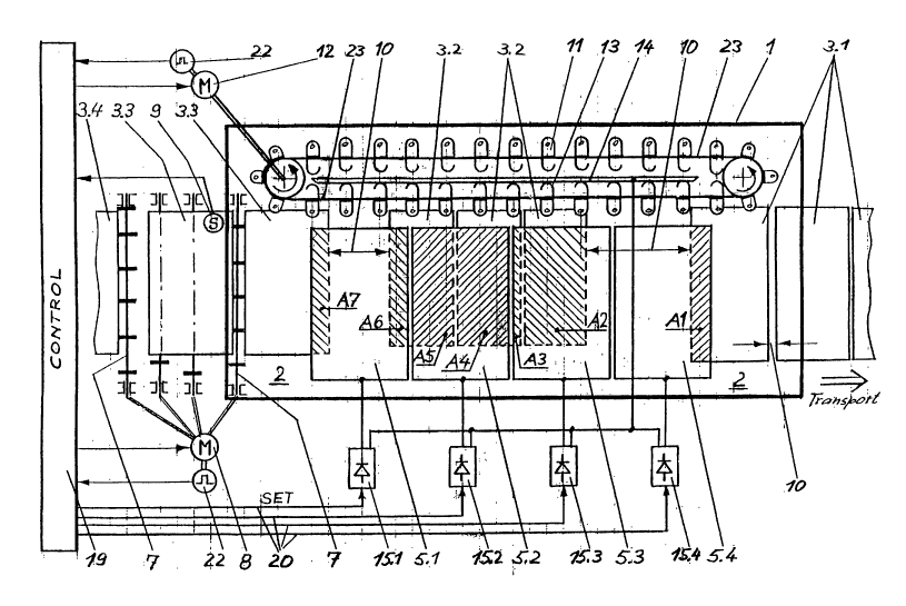
Fig. 3 is a schematic top view of a horizontal conveyorized system. For
simplification sake, the plant has been represented with only four upper
counter electrodes 5.x (5.1, 5.2, 5.3, 5.4) and with the associated
electrolyte
25 cell rectifiers 15.x (15.1, 15.2, 15.3, 15.4). In practice, such a system
is
comprised of up to 20 upper and 20 lower counter electrodes 15.x, 16.x, i.e.,
of
20 anode pairs. In the system shown in Fig. 3, there are three different kinds
of
printed circuit boards 3.x (3.1, 3.2, 3.3), i.e., columns of different printed
circuit
boards 3.x. Another printed circuit board 3.4 is just in front of the plant.
The
printed circuit boards 3.x are conveyed through the plant in the direction of
transport (shown by the arrow).
CA 02454267 2004-O1-16
WO 03/038159 PCT/EP02/11764
26
It may be surveyed therefrom that there are printed circuit boards 3.x of
various
board formats spaced different distances apart inside the conveyorized system,
i.e., the gaps 10 between the printed circuit boards 3.x have various sizes.
The
respective electrolytic effective surface areas Ax (A1, A2, A3, A4, A5, A6,
A7),
which overlap with the respective one of the anodes 5.x, are shown in hatched
line. These surface areas are the surface areas Ax which presently are located
below the anodes 5.x. These projections constitute an instantaneous view.
They vary constantly in function of the forward feed. The surface areas are
constantly recalculated, e.g., after a forward feed of 2.5 - 60 mm or in time
intervals of 500 msec - 20 sec.
The sum of the surface areas Ax presently located within the region of an
anode multiplied by the set point of the current density yields the bath
current
the electrolyte cell rectifiers 15.x have to set at the moment. In practice it
proved to be a very good value to update the bath current after a forward feed
of approximately 10 mm. Accordingly, at a transportation speed of 2 m/min, all
of the rectifier currents are to be updated approximately 3 times a second.
This
may be realized at low cost with the control systems available. The current
varies in small steps. With previous calculation it is also possible to
continuously vary the electric current. In this case, the electrolyte cell
rectifiers
15.x are continuously triggered with a reference current value signal.
Usually,
this is an analog value.
In Fig. 3, only area A1 is presently located under the anode 5.4. The areas A2
and A3 are located directly opposite the anode 5.3. The areas A4 and A5 are
located directly opposite the anode 5.2 and the areas A6 and A7 are located
under the anode 5.1. The printed circuit boards 3.1 and 3.2 are spaced one
counter electrode length apart in the direction of transport. This permits to
set
various current densities for the printed circuit boards 3.1 and 3.2 without
any
disadvantage. The printed circuit boards 3.2 and 3.3 are conveyed separated
by gaps that are smaller than the length of the anode. Due to the small gaps,
the current density for these printed circuit boards 3.2, 3.3 cannot be varied
CA 02454267 2004-O1-16
WO 03/038159 PCT/EP02/11764
27
because these printed circuit boards 3.2 and 3.3 are momentarily located
below or above the same anode 5.1. Position sensor 9 senses the size of the
gaps. The gaps are taken into consideration in the instantaneous computation
of the surface area in the control unit 19.
If various printed circuit board products are to be processed at the same
current density for different lengths of time, the transportation speed of the
printed circuit boards 3.x is varied. In practice, this is carried out when
the
boundary transition line between the two columns of printed circuit boards
that
are to be processed in different manners is located approximately in the
center
of the conveyorized system. In for example increasing the speed, the leading
printed circuit boards 3.2 (those being advanced in front of the boundary
transition line) are processed in too short periods of time. This is
compensated
for by a temporary specific increase in the current density in that region of
the
system in which the printed circuit boards 3.2 are located until there are
only
trailing printed circuit boards 3.3 left in the conveyorized system. If the
speed is
reduced, the current density of the corresponding anodes 5.4 is automatically
temporarily reduced accordingly. It is hereby no longer necessary to run the
conveyorized system without charge, as this was the case hereto before.
In practice, a change in product during the charging of a conveyorized system
is foreseeable. Therefore, a gap 10 of at least one counter electrode length
between two columns of printed circuit boards is controllably met when the
printed circuit board products are to be processed at various current
densities.
Again, the conveyorized system needs no longer be run without charge.
Unplanned gaps 10 between the printed circuit boards 3.x, as they occur in
practice are not foreseeable, though. Printed circuit boards may for example
be
removed from the column for test purposes or there is a jam in the plant
occasioned by disturbances, the boards 3.x being shifted over each other as a
result thereof. In realizing the present invention, the printed circuit boards
3.x
located in front of or behind a gap 10 are no longer scrap.
CA 02454267 2004-O1-16
WO 03/038159 PCT/EP02/11764
28
When the sequence of the printed circuit boards 3.x does not change after they
have entered the charging station of the plant, the corresponding
(overlapping)
anode and printed circuit board (cathode) surface areas in every electrolytic
cell are known at all times. These data are calculated and stored at all times
in
the main control unit to compute the actual electrolyte cell rectifier set
points of
the electric currents and the current ramps. In every electrolyte cell
rectifier
15.x, the momentarily required processing current is set by controlling and
adjusting means known in the measuring and control technique. In order for
these electric currents to be distributed evenly over the surfaces of the
printed
circuit boards 3.x and for their edges not to be preferentially processed, a
small
enough anode-cathode spacing is selected in the electrolytic cells - as
described herein above.
The anodes may be configured to be non-segmented or to be segmented
transverse to the direction of transport (not illustrated herein). In the case
of a
segmented anode, each anode segment is allocated to an individual electrolyte
cell rectifier. The momentarily corresponding surface areas of the printed
circuit
boards 3.x are also calculated individually for each anode segment. In turn,
the
set points of the electric current values for the electrolyte cell rectifiers
are
formed therefrom. As the number of electrolyte cell rectifiers in a
conveyorized
system increases, it is appropriate to provide the electrolyte cell rectifiers
15.x
with a control link to the main control unit 19 via a serial bus system such
as
Profibus or Ethernet.
If printed circuit boards 3.x are to be electrolytically metal-plated that are
provided with a very thin copper cladding bof a thickness ranging from 0.5 -
5 pm, the invention may also be used to limit the initial current density in
order
to avoid burns for example. By means of the data stored in the control unit
19,
the initial current density can be set to a reduced value by means of a
correction factor. As metal-plating progresses, the current density may be
dynamically adjusted in one or several steps or continuously up to the nominal
current density in accordance with the increase in thickness of the conductive
CA 02454267 2004-O1-16
WO 03/038159 PCT/EP02/11764
29
layer in order to permit fast and high-quality buildup of layers on the
surface of
the printed circuit boards.
Position sensor 9 may be located inside or outside the plating tank 1. If the
sensor 9 is located inside the plating tank 1, it must be resistant to the
electrolyte used. If it is positioned in proximity to the point where the
clamps
grasp the printed circuit boards 3.x, the sensor 9 also senses errors in
transport that may occur between the admission of the printed circuit boards
3.x in the conveyorized system and the reaching of the clamps 11. A common
motor 8,12 with a drive sensor 22 as shown in Fig. 2 may also be substituted
for the driving motors 8 and 12 shown in the Figs. 1 and 3. In this case, the
control measures for synchronizing the roll driving motor 8 and the clamp
driving motor 12 are not applicable.
The invention is not only suited for the electrolytic processing of electrical
printed circuit boards but also for processing work that is to be
electrolytically
metal-plated, etched or processed in any other way on only one surface side.
Further, it is also unrestrictedly suited for vertical conveyorized system in
which
the work is transported and processed in a vertical orientation and in a
horizontal direction of transport.
It will be understood that the examples and embodiments described herein are
for illustrative purpose only and that various modifications and changes in
light
thereof as well as combinations of features described in this application will
be
suggested to persons skilled in the art and are to be included within the
spirit
and purview of the described invention and within the scope of the appended
claims. All publications, patents and patent applications cited herein are
hereby
incorporated by reference.
CA 02454267 2004-O1-16
WO 03/038159 PCT/EP02/11764
Listing of numerals:
1 plating tank
5 2 electrolyte
3, 3.1, 3.2, 3.3, 3.4, 3.x work, work pieces, e.g., printed
circuit boards
4 level of the electrolyte
5, 5.1, 5.2, 5.3, 5.4, 5.x upper anode, counter electrode
6, 6.1, 6.2, 6.3, 6.4, 6.x lower anode, counter electrode
10 7 transport roll, transport wheel
shaft
3 roll driving motor
position sensor
10 gap between printed circuit boards
11 clamp
15 12 clamp driving motor
13 sliding contact
14 sliding rail
15, 15.1, 15.2, 15.3, 15.4,upper electrolyte cell rectifier,
15.x current source
16, 16.1, 16.2, 16.3, 16.4,lower electrolyte cell rectifier,
16.x current source
20 17 ion permeable insulator
18 isolating strip
19 main control unit
20 control lines
21 electrolytic cell
25 22 drive sensor
23 conveying belt, chain
A1, A2, A3, A4, A5, A6, electrolytically active surface
A7, Ax area