Note: Descriptions are shown in the official language in which they were submitted.
CA 02454269 2012-02-27
,1*
WO 03/032397 =
PCT/US02/23056
=
1
P0212US-7
PATENT
-
INSULATING GATE AlGaN/GaN HEW
=
=
. .
= = =
= =
BACKGROUND OF me INVENTION
Field of the Invention
This invention relates to aluminum gallium nitride
=
and gallium nitride based high electron mobility
transietors.
Description of the Related Art
Microwave systems commonly use solid state
transistors as amplifiers and. oscillators which has .
resulted in significantly reduced system size and
increased reliability. To accommodate the expanding.
number of microwave systems, there is an interest in
increasing their operating frequency and power. Higher
frequency signals can carry more information (bandwidth),
allow for smaller antennas with very high gain, and
1 .
provide radar with improved resolution.
Field effect transistors (FETs) and high electron
mobility transistors (HEMTs) are common types of solid
state transistors that are fabricated from semiconductor
'
CA 02454269 2004-01-16
WO 03/032397
PCT/US02/23056
2
materials such as Silicon (Si) or Gallium Arsenide
(GaAs). One disadvantage of Si is that it has low
electron mobility (approximately 1450 cm2/V-s), which
produces a high source resistance. This resistance
seriously degrades the high performance gain otherwise
possible from Si based HEMTs. [CRC Press, The Electrical
Engineering Handbook, Second Edition, Dorf, p.994,
(1997)]
GaAs is also a common material for use in HEMTs and
has become the standard for signal amplification in civil
and military radar, handset cellular, and satellite
communications. GaAs has a higher electron mobility
(approximately 6000 cm2/V-s) and a lower source resistance
than Si, which allows GaAs based devices to function at
higher frequencies. However, GaAs has a relatively small
bandgap (1.42 eV at room temperature) and relatively
small breakdown voltage, which prevents GaAs based HEMTs
from providing high power at high frequencies.
Improvements in the manufacturing of gallium nitride
(GaN) and aluminum gallium nitride (AlGaN) semiconductor
materials have focused interest on the development of
AlGaN/GaN based HEMTs. These devices can generate large
amounts of power because of their unique combination of
material characteristics including high breakdown fields,
wide bandgaps (3.36 eV for GaN at room temperature),
large conduction band offset, and high saturated electron
drift velocity. The same size AlGaN/GaN amplifier can
produce up to ten times the power of a GaAs amplifier
operating at the same frequency.
U.S. Patent number 5,192,987 to Khan et al discloses
AlGaN/GaN based HEMTs grown on a buffer and a substrate,
CA 02454269 2004-01-16
WO 03/032397
PCT/US02/23056
3
and a method for producing them. Other HEMTs have been
described by Gaska et al., "High-Temperature Performance
of AlGaN/GaN HFET's on SIC Substrates," IEEE Electron
Device Letters, Vol. 18, No 10, October 1997, Page 492;
and Wu et al. "High Al-content AlGaN/GaN HEMTs With Very
High Performance", IEDM-1999 Digest pp. 925-927,
Washington DC, Dec. 1999. Some of these devices have
shown a gain-bandwidth product (fT) as high as 100
gigahertz (Lu et al. "AlGaN/GaN HEMTs on SIC With Over
100 GHz ft and Low Microwave Noise", IEEE Transactions on
Electron Devices, Vol. 48, No. 3, March 2001, pp. 581-
585) and high power densities up to 10 W/mm at X-band (Wu
et al., "Bias-dependent Performance of High-Power
AlGaN/GaN HEMTs", IEDM-2001, Washington DC, Dec. 2-6,
2001)
Despite these advances, AlGaN/GaN based FETs and
HEMTs have been unable to produce significant amounts of
total microwave power with high efficiency and high gain.
They produce significant power gain with DC gate drives,
but with frequency step-ups as low as a millihertz to a
few kilohertz, their amplification drops off
significantly.
It is believed that the difference between AC and DC
amplification is primarily caused by surface traps in the
device's channel. Although the nomenclature varies
somewhat, it is common to refer to an impurity or defect
center as a trapping center (or simply trap) if, after
capture of one type of carrier, the most probable next
event is re-excitation.
At equilibrium, the traps donate electrons to the 2-
dimensional electron gas (2-DEG) in HEMTs. Trapping
CA 02454269 2004-01-16
WO 03/032397
PCT/US02/23056
4
levels located deep in a band gap are also slower in
releasing trapped carriers than other levels located near
the conduction of valence bands. This is due to the
increased energy that is required to re-excite a trapped
electron from a center near the middle of the band gap to
the conduction band, compared to the energy required to
re-excite the electron from a level closer to the
conduction band.
AlxGai_xN (X=0-1) has a surface trap density
comparable to the channel charge of the transistor with
the traps in deep donor states with activation energy
ranging from 0.7 to 1.8 eV (depending on X). During HEMT
operation, the traps capture channel electrons. The slow
trapping and de-trapping process degrades transistor
speed, which largely degrades the power performance at
microwave frequencies.
It is believed that the trap density of a AlGaN/GaN
based HEMTs is dependent upon the surface and volume of
the AlGaN layer. Reducing the thickness of the AlGaN
layer reduces the total trapping volume, thereby reducing
the trapping effect during high frequency operation.
However, reducing the thickness of the AlGaN layer can
have the undesirable effect of increasing the gate
leakage. During normal operation a bias is applied across
the source and drain contacts and current flows between
the contacts, primarily through the 2DEG. However, in
HEMTs having thinner AlGaN layers, current can instead
leak into the gate creating an undesirable current flow
from the source to the gate. Also, the thinner AlGaN
layer can result in a reduction in the HEMT's available
maximum drive current.
CA 02454269 2004-01-16
WO 03/032397
PCT/US02/23056
SUMMARY OF THE INVENTION
The present invention seeks to provide an improved
AlGaN/GaN HEMT that addresses the above problems by
5 having a thin AlGaN layer to reduce trapping and also
having additional layers to reduce gate leakage and
increase the maximum drive current. The invention also
discloses methods for manufacturing HEMTs with these
characteristics.
One HEMT according to the present invention
comprises a high resistivity semiconductor layer with a
barrier semiconductor layer on it. The barrier layer has
a wider bandgap than the high resistivity layer and a two
dimensional electron gas forms between the barrier and
high resistivity layers. Source and drain contacts are
included that contact the barrier layer, with part of the
surface of the barrier layer uncovered by the contacts.
An insulating layer is included on the uncovered surface
of the barrier layer. A gate contact is deposited on the
insulating layer with the insulating layer forming a
barrier to gate leakage current and also increasing the
HEMT's maximum current drive.
The invention also includes methods for fabricating
HEMTs according to the present invention. In one method,
the active layers of the HEMT are formed on a substrate
in a metal-organic chemical vapor deposition reactor.
Source gasses are then fed into the reactor for "in-situ"
formation of an insulating layer on the active HEMT's
active layer. The HEMT can then be removed from the
reactor for further processing.
CA 02454269 2004-01-16
WO 03/032397
PCT/US02/23056
6
Another method for fabricating HEMTs according to
the present invention includes forming the active layers
of a HEMT on a substrate. The substrate is then placed in
a sputtering chamber where the insulating layer is
sputtered onto the top surface of the HEMT active layers.
The HEMT can then be removed from the sputtering chamber
for further processing.
These and other further features and advantages of
the invention would be apparent to those skilled in the
art from the following detailed description, taking
together with the accompanying drawings, in which:
BRIEF DESCRIPTION OF THE DRAWINGS
FIG. 1 is a sectional view of a AlGaN/GaN HEMT
according to the present invention having an insulating
layer on the AlGaN layer and' a gate contact on the
insulating layer;
FIG. 2 is a sectional view of the HEMT in FIG. 1
with a dielectric layer on its surface;
FIG. 3 is a sectional view of a AlGaN/GaN HEMT
according to the present invention with the insulating
layer only under the gate contact;
FIG. 4 is a sectional view of a AlGaN/GaN HEMT
according to the present invention having a double
insulating layers on the AlGaN layer and a gate contact
on the insulating layers;
FIG. 5 is a sectional view of the HEMT in claim 4
with a dielectric layer on its surface;
FIG. 6 is a sectional view of a AlGaN/GaN HEMT
according to the present invention with the double
insulating only under the gate contact;
CA 02454269 2004-01-16
WO 03/032397
PCT/US02/23056
7
FIG. 7 is a simplified diagram of a metal-organic
chemical vapor deposition (MOCVD) reactor used in a
method according to the present invention for fabricating
a HEMT; and
FIG. 8 is a simplified diagram of a sputtering
chamber used in a method according to the present
invention for fabricating a HEMT.
DETAILED DESCRIPTION OF THE INVENTION
FIG. 1 shows an AlGaN/GaN based HEMT 10 constructed
in accordance with this invention. It comprises a
substrate 11 that can be either sapphire (A1203) or
silicon carbide (SIC), with the preferred substrate being
a 4H polytype of silicon carbide. Other silicon carbide
polytypes can also be used including 3C, 6H and 15R
polytypes. An AlõGaiN buffer layer 12 (where x in between
0 and 1) is included on the substrate 11 and provides an
appropriate crystal structure transition between the
silicon carbide substrate and the remainder of the HEMT
10. Many different materials can be used for the buffer
layer 12 with a suitable material for a buffer layer on
SIC being AlõGal_xN, with x = 1.
Silicon carbide has a much closer crystal lattice
match to Group III nitrides than sapphire and results in
Group III nitride films of higher quality. Silicon
carbide also has a very high thermal conductivity so that
the total output power of Group III nitride devices on
silicon carbide is not limited by the thermal dissipation
of, the substrate (as is the case with some devices formed
on sapphire). Also, the availability of semi insulating
silicon carbide substrates provides the capacity for
CA 02454269 2004-01-16
WO 03/032397
PCT/US02/23056
8
device isolation and reduced parasitic capacitance that
make commercial devices possible. SiC substrates are
available from Cree Research, Inc., of Durham, North
Carolina and methods for producing them are set forth in
the scientific literature as well as in a U.S. Patents,
Nos. Re. 34,861; 4,946,547; and 5,200,022.
The HEMT 10 includes a high resistivity layer 20 on
the buffer layer 12 and a barrier layer 18 on said high
resistivity layer 20 such that the high resistivity
layer 20 is sandwiched between the barrier layer 18 and
the buffer layer 12. The barrier layer 18 is typically
about 0.1 to 0.3 micrometers thick and the barrier layer
18, high resistivity layer 20, and buffer layer 12, are
preferably formed on the substrate 11 by epitaxial growth
or ion implantation.
The HEMT also includes source and drain contacts 13,
14 that are on the surface of the high resistivity layer
20. The barrier layer 18 is disposed between the contacts
13 and 14, with each contacting the edge of the barrier
layer. An insulating layer 24 is included on the barrier
layer 18 between the contacts 13 and 14. In the
embodiment shown, the insulating layer 24 covers the
entire barrier layer 18, but in other embodiments (one
described below) all of the barrier layer 18 is not
covered. The layer 24 can be made of many different
materials including but not limited to silicon nitride
(SiN), aluminum nitride (A1N), silicon dioxide (Si02) or a
combination incorporating multiple layers thereof.
The contacts 13 and 14 are usually separated by a
distance in the range 1.5 to 10 micrometers for microwave
devices. A rectifying Schottky contact (gate) 16 is
CA 02454269 2004-01-16
WO 03/032397 PCT/US02/23056
9
located on the surface of the insulator layer 24 between
the source and drain contacts 13 and 14, and it typically
has a length in the range of 0.1 to 2 micrometers. The
total width of the HEMT depends on the total power
required. It can be wider than 30 millimeters, with the
typical width being in the range of 100 microns to 6
millimeters.
The AlGa1N layer 18 has a wider bandgap than the
GaN layer 20 and this discontinuity in energy band gaps
results in a free charge transfer from the wider band gap
to the lower band gap material. A charge accumulates at
the interface between the two and creates a two
dimensional electron gas (2DEG) 22 that allows current to
flow between the source and drain contacts 13 and 14. The
2DEG has very high electron mobility which gives the HEMT
a very high transconductance at high frequencies. The
voltage applied to the gate 16 electrostatically controls
the number of electrons in the 2DEG directly under the
gate, and thus controls the total electron flow.
The source and drain contact 13 and 14, are
preferably formed of alloys of titanium, aluminum, nickel
and gold, and the gate 16 is preferably formed of
titanium, platinum, chromium, nickel, alloys of titanium
and tungsten, and platinum silicide. In one embodiment,
the contacts comprise an alloy of nickel, silicon, and
titanium that is formed by depositing respective layers
of these materials, and then annealing them. Because this
alloy system eliminates aluminum, it avoids unwanted
aluminum contamination over the device surface when the
anneal temperature exceeds the melting point of aluminum
(660 degrees C).
CA 02454269 2004-01-16
WO 03/032397
PCT/US02/23056
During operation, the drain contact 14 is biased at
a specified potential (positive drain potential for an n-
channel device) and the source is grounded. This causes
current to flow through the channel and 2DEG, from the
5 drain to the source contacts 13, 14. The flow of current
is controlled by the bias and frequency potentials
applied to the gate 16, which modulate the channel
current and provide gain.
As described above, the trap density of the AlGaN
10 layer 18 is dependent on the layer's volume and by
reducing the thickness of the layer 18 the trapping
density can also be reduced to decrease the trapping
effect. However, reducing the thickness of the AlGaN
layer increases gate leakage and reduces the devices
maximum current drive.
By having the insulating layer between the gate 16
and the barrier layer 18, gate leakage of the HEMT is
reduced. This has the direct impact of improving the
long-term reliability of the device, since gate leakage
is one of the sources of HEMT degradation. The turn-on
voltage of the HEMT 10 is dependent upon the type of
material used for the insulator layer 24 and the turn-on
voltage can be as high as 3-4 volts. The HEMT 10 can then
be operated in the accumulation mode with higher current
level and higher input drive level. The insulator layer
also serves as a natural passivant for the HEMT, which
improves its reliability.
FIG. 2 shows an AlGaN based HEMT 30 similar to the
HEMT 10 in FIG. 1. The HEMT 30 has similar layers
including a substrate 11, buffer layer 12, GaN layer 20,
2DEG 22, AlxGal_.N barrier layer 18 and insulating layer
=
CA 02454269 2004-01-16
WO 03/032397
PCT/US02/23056
11
24. The HEMT 30 also has source, gate and drain contacts
13, 14, 16, similar to those'on the HEMT 10. The HEMT 30
includes an additional dielectic layer 32 disposed on the
surface of the insulating layer 24 between the source,
gate and drain contacts 13, 16, 14. The dielectric layer
protects the HEMT from undesirable passivation,
impurities and damage that can occur during handling. The
dielectric layer can be made of many different materials
or combinations of materials, with a suitable material
being Si,Ny.
The insulating layer 24 serves to reduce gate
leakage and allow increased current drive by the section
of the layer 24 that is sandwiched between the gate 16
and the barrier layer 18. The sections of the layer 24
that extend beyond the gate 16 help in protecting the
surface of the barrier layer between the contacts, but do
not help in reducing gate leakage or increasing current
drive.
FIG. 3 shows another embodiment of a HEMT 40
according to the present invention similar to the HEMTs
10 and 30 in FIGs. 1 and 2. The HEMT 40 has similar'
layers including a substrate 11, buffer layer 12, GaN
layer 20, 2DEG 22 and Al.Gal,,N barrier layer 18. The HEMT
also has source, gate and drain contacts 13, 14 and
25 16, similar to those on the HEMTs 10 and 40. However, the
insulating layer 42 in HEMT 40 is only included below the
gate contact 16, such that the insulating layer is only
sandwiched between the gate contact 16 and the barrier
layer 18. The surface of the barrier layer 18 between the
30 contacts 13, 14, 16, is uncovered by the insulating layer
42. It can remain uncovered or can include a layer of
CA 02454269 2004-01-16
WO 03/032397
PCT/US02/23056
12
dielectic material 44 to help reduce the effects of
trapping and to help reduce any undesirable passivation
and damage to the HEMT's layers. It also helps to reduce
the introduction of impurities into the HEMT's layers.
The dielectric layer is preferably silicon nitride
(SiõNy) , with silicon being the source of the donor
electrons to reduce trapping. To be most effective the
layer 22 and 44 should meet the following conditions.
First, it should have a dopant that provides a high
source of donor electrons. For silicon nitride, the layer
should have a high percentage of Si. Although the
applicant does not wish to be bound by any theory of
operation, it is presently believed that electrons from
the layer fill surface traps such that they become
neutral and do not capture barrier layer electrons during
operation.
Second, the energy level of the dopant should be
higher than the energy level in the trap and for optimal
results, the energy should be higher than the energy
level of the barrier layer's conduction band edge. It is
believed that this reduces the possibility of an electron
from the gate metal giving to the donor states and
prevents the trapping and de-trapping at that energy
level. The layer will also work if the dopant's energy
level is slightly below the energy level in the barrier
layer's conduction band, but the higher its energy the
better.
Third, there should be little or no damage to the
device's surface and the forming of the dielectric layer
should not increase the surface damage. It is believed
that surface damage can create more surface traps.
CA 02454269 2004-01-16
WO 03/032397
PCT/US02/23056
13
Fourth, the bond between the coating and the surface of
the conducting channel should be stable under stress. If
the bond is unstable, it is believed that the layer may
fail under actual device operation when subjected to the
stress created by increases - in the electron field,
voltage or temperature.
Low breakdown voltage can be experienced in HEMTs
that have an insulating layer that is deposited in-situ
using metal-organic chemical vapor deposition (MOCVD).
Although applicants do not wish to be bound by any one
theory, it is believed that this low breakdown voltage is
attributable to the doping/degradation of the AlGaN
barrier layer during growth of the SiN layer. The growth
conditions such as the -growth temperature of the SiN
layer also affected the mobility of the HEMT's sheet
charge. Lowering the growth temperature of the insulating
layer resulted in less degradation of the HEMT, but also
resulted in a reduced growth rate of the SiN.
To allow for the growth of an insulating layer at a
normal growth rate without doping or degrading the AlGaN
barrier layer, a double insulating layer arrangement can
be used instead of the single insulating layer. FIG. 4
shows a HEMT 50 that is similar to the HEMTS 10, 30 and
40 in FIGs. 1, 2 and 3. The HEMT 50 has a similar
substrate 11, buffer layer 12, GaN layer 20, 2DEG 22, and
Al,Gai.N barrier layer 18. The HEMT 30 also has similar
source, gate and drain contacts 13, 14, 16. However, the
HEMT 50 has a double layer arrangement is used instead of
a single layer. The double layers include an AlN spacer
layer 52 on the barrier layer 18 between the source and
drain contacts 13, 14. A SiN insulating layer 54 is
CA 02454269 2004-01-16
WO 03/032397
PCT/US02/23056
14
included on the AIN layer 52 with the gate contact 16
arranged on the insulating layer 54.
The AIN spacer layer 52 serves as a spacer or '
barrier between the SiN insulating layer 52 and the
active AlGaN barrier layer 18. This spacer layer 52
prevents the doping/degradation of the barrier layer 18
during growth of the SiN insulating layer 54 during
normal growth conditions.
Other materials can be used for the spacer layer as
long as the material prevents the doping and degradation
of the AlGaN barrier layer 18 during deposition of the
SiN insulating layer 54 at normal growth rates. Methods
that allow for depositing the SiN insulating layer
directly on the AlGaN layer without a spacer layer can
also be used if doping and degradation can be avoided.
The important aspect of these features of the invention
is that the HEMTs low breakdown voltage is avoided.
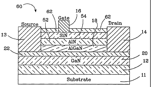
FIG. 5 shows another HEMT 60 according to the
present invention that is similar to the HEMT 50 of FIG.
4 having a similar substrate 11, buffer layer 12, GaN
layer 20, 2DEG 22, AlxGalõP barrier layer 18, AIN spacer
layer 52 and SiN insulating layer 54. The HEMT 60 also
has similar source, gate and drain contacts 13, 14 and
16. The HEMT 60 also includes a dielectric layer 62 over
the exposed surface of the SiN insulating layer 54
between the contacts 13, 14, 16,, similar to the
dielectric layer 32 of the HEMT 30 in FIG. 2. Just as
layer 32 in HEMT 30, the dielectric layer 54 helps
protect the HEMT 60 from undesirable passivation,
impurities and damage that can occur during handling. The
dielectric layer can be made of many different materials
CA 02454269 2004-01-16
WO 03/032397
PCT/US02/23056
or combinations of materials, with a suitable material
being Si,Ny.
FIG. 6 shows another HEMT 70 according to the
present invention that, similar to the HEMT 40 in FIG. 3,
5
which has an insulating layer only below the gate
contact. The HEMT 70 has a similar substrate 11, buffer
layer 12, GaN layer 20, 2DEG 22, AlxGai_xN barrier layer 18
and source, gate and drain contacts 13, 14 and 16. The
HEMT's SiN insulating layer 72 and AIN spacer layer 74
10
are only included below the gate 16, such that both are
sandwiched between the gate 16 and the barrier layer 18.
In another embodiment (not shown) the spacer layer 74 can
extend beyond the gate to cover the surface of the
barrier layer between the contacts 13, 14 and 16.
15
The HEMT 70 also includes a dielectric layer 76 that
as shown covers the surface of the barrier layer 18
between the contacts 13, 14 and 16. As with the
dielectric layer 44 in the HEMT 40 of FIG. 3, the
dielectic layer 76 helps reduce the effects of trapping
and helps reduce the undesirable passivation and damage
to the HEMT's layers. It also helps to reduce the
introduction of impurities into the HEMT's layers. The
dielectric layer 76 is preferably silicon nitride (SixNy),
with silicon being the source of the donor electrons to
fill any traps. To be most effective the layer 76 should
meet the four conditions described above for dielectric
layer 44 of FIG. 3.
The active layers of the HEMTs described above are
made from AlGaN/GaN, but they can also be made of other
Group III nitride materials. Group III nitrides refer to
those semiconductor compounds formed between nitrogen and
CA 02454269 2004-01-16
WO 03/032397
PCT/US02/23056
16
the elements in Group III of the periodic table, usually
aluminum (Al), gallium (Ga), and indium (In). The term
also refers to ternary and tertiary compounds such as
AlGaN and AlInGaN.
Methods of Manufacturing
The present invention also discloses methods for
fabricating the HEMTs above with single or double
insulating layer. The insulating layers can be deposited
on the AlGaN/GaN semiconductor material using MOCVD,
plasma chemical vapor deposition (CVD), hot-filament CVD
or sputtering.
FIG. 7 shows a MOCVD reactor 80 used in the new
method to grow the AlGaN/GaN active layers on a substrate
and to deposit the insulating layers. The reactor 80
comprises a reaction chamber 82 having growth platform 84
supported by a rotary shaft 86. In most applications a
substrate 88 such as either sapphire (A1203) or silicon
carbide (SiC) sapphire is disposed on the growth platform
84, although other substrates can also be used.
During growth, the platform 84 is heated by heater
elements 90 to maintain substrate 88 at a predetermined
temperature. The temperature is typically between 400
and 1200 degrees centigrade ( C), but can be higher or
lower depending on the type of growth desired. The heater
elements 90 can be a variety of heating devices but is
usually a radio frequency (RF) or resistance coil.
A carrier gas 92 is supplied to a gas line 94, the
carrier gas being hydrogen or nitrogen. The carrier gas
92 is also supplied through mass flow controllers 95a,
CA 02454269 2004-01-16
WO 03/032397
PCT/US02/23056
17
95b, 95c, to respective bubblers 96a, 96b, 96c. Bubbler
96a has a growth compound, typically an alkylated
compound having a methyl or ethyl group, e.g. trimethyl
gallium TMG), trimethyl aluminum (TMA) or trimethyl
indium (TMI). Bubblers 96b and 96c may also contain a
similar metalorganic compound to be able to grow an alloy
of a Group III compound. The bubblers 96a, 96b, 96c are
typically maintained at a predetermined temperature by
constant temperature baths 98a, 98b, 98c to ensure a
constant vapor pressure of the metal organic compound
before it is carried to the reaction chamber 82 by the
carrier gas 92.
The carrier gas 92 which passes through bubblers
96a, 96c, 96c is mixed with the carrier gas 92 flowing
within the gas line 94 by opening the desired combination
of valves 100a, 100b, 100c. The mixed gas is then
introduced into the reaction chamber 82 through a gas
inlet port 102 formed at the upper end of the reaction
chamber 82.
A nitrogen containing gas 104 such as ammonia is
supplied to the gas line 94 through a mass flow
controller 106. The flow of nitrogen containing gas is
controlled by valve 108. If the carrier gas 92 is mixed
with the nitrogen containing gas 104, and the TMG vapor
within the gas line 94 is introduced into the reaction
chamber 82, the elements are present to grow gallium
nitride on the substrate 88 through thermal decomposition
of the molecules in the TMG and ammonia containing gas.
To dope alloys of gallium nitride on the substrate
88, one of the bubblers 96a, 96b, 96c not being used for
the TMG is used for a dopant material, which is usually
CA 02454269 2004-01-16
WO 03/032397
PCT/US02/23056
18
Magnesium (Mg) or Silicon (Si), but can be other material
such as beryllium, calcium, zinc, or carbon. Bubbler 96b
or 96c is used for an alloy material such as boron,
aluminum, indium, phosphorous, arsenic or other
materials. Once the
dopant and alloy are selected and
the appropriate valve 100a, 100b, 100c is opened to allow
the dopant to flow into gas line 94 with the gallium and
nitrogen containing gas 104, the growth of the doped
layer of gallium nitride takes place on substrate 88.
The gas within the reaction chamber 82 can be purged
through a gas purge line 110 connected to a pump 112
operable under hydraulic pressure.
Further, a purge
valve 114 allows gas pressure to build up or be bled off
from the reaction chamber 82.
The growth process is typically stopped by shutting
off the gallium and dopant sources by closing valves 100a
and 100b, and keeping the nitrogen containing gas and the
carrier gas flowing. Alternatively, the reaction chamber
82 can be purged with a gas 116 that can be controlled
through a mass flow controller 118 and valve 120. The
purge is aided by opening valve 114 to allow the pump 112
to evacuate the reaction chamber 82 of excess growth
gasses. Typically, the purge gas 116 is hydrogen, but can
be other gasses. Turning off power to the heater elements
90 cools the substrate 88.
In one method according to the present invention,
the application of the insulating layer/layers occurs
after growth of the AlGaN/GaN semiconductor material and
prior to or during cooling of the reaction chamber 82
(referred to as in-situ). Following growth of the
semiconductor material in a reactor chamber 82, the flow
CA 02454269 2004-01-16
WO 03/032397
PCT/US02/23056
19
of undesired growth gasses is discontinued by closing the
appropriate combination of valves 100a, 100b, 100c.
A
short purge of the reactor may be completed to remove the
undesirable gasses as described above. Gasses are then
flowed into the reactor to deposit the insulating
layer(s) and in a preferred method, the gasses used for
the insulating layer(s) are provided from typical MOCVD
sources. When depositing a Si3N4 insulating layer on the
AlGaN/GaN semiconductor material, disilane (Si2H6) and
ammonia (NH6) are introduced into the reactor chamber 82,
through gas line 94. The molecules are now present to
deposit the Si3N4 through thermal decomposition on the
AlGaN/GaN material. When depositing double insulating
layers, the appropriate gasses are introduced into the
chamber to form the AIN layer prior to forming the Si3N4
layer.
In those embodiments of the HEMT having a dielectric
layer, the dielectric layer can also be deposited in -
situ. Examples of some of the compounds that can be used
in the dielectric layer include Si, Ge, MgO, MgNõ, ZnO,
SIN., Si0õ, Sc0x, GdOõ and alloys thereof. Multiple layers
and repeated stacks of layers of suitable materials can
be used as barrier layers as well, such as SiNx/Si,
MgNx/SiN, or MgNõ/Mg0,. The different barrier layers can
be formed from the following source gasses: Si from
silane or disilane, Ge from germane, MgNõ from
cyclopentadienyl magnesium or methyl-cyclopentadienyl
magnesium and ammonia, MgO from cyclopentadienyl
magnesium or methyl-cyclopentadienyl magnesium and
nitrous oxide, ZnO from dimethyl zinc or diethyl zinc and
nitrous oxide or water, SiN, from silane or disilane and
CA 02454269 2004-01-16
WO 03/032397
PCT/US02/23056
ammonia or nitrous oxide, and SiOx formed from silane or
disilane and nitrous oxide.
After the insulating and dielectric layers are
deposited the semiconductor material can be cooled in the
5 reaction chamber 82. The semiconductor material can then
be removed from the cooled reaction chamber 82. When the
structure is ready for additional processing such as
metalization, the portion of the layers can be removed by
a number of different methods including but not limited
10 to wet chemical hydrofluoric acid (HF) etching, reactive
ion etching, or plasma etching.
Another method for depositing the insulating layers
according to the present invention is through sputtering.
FIG. 8 shows a simplified sputtering chamber 130 that can
15 be used to deposit material on a substrate. In operation,
a semiconductor device 132 is placed on an anode 134. The
chamber 136 is then evacuated and an inert gas 138 such
as argon is fed into gas line 140 and bled through the
valve 142 to maintain a background pressure. A cathode
20 144 made of the material to be deposited on the
substrate/device, is positioned within the chamber 136.
With the application of a high voltage 146 between the
electrodes, the inert gas is ionized and the positive
ions 148 excel to the cathode 144. On striking the
cathode 144, they collide with the cathode atoms 150,
giving them sufficient energy to be ejected. The
sputtered cathode atoms 150 travel through space,
eventually covering the anode 134 and the semiconductor
device 132 with a coating 133 from the sputtered atoms
150.
CA 02454269 2004-01-16
WO 03/032397 PCT/US02/23056
21
Other sputtering units can be more complex and
detailed, but they work on much the same basic physical
mechanisms. Using the more complex sputtering systems, it
is possible to sputter and deposit a range of metals and
dielectric layers.
The sputtering method can be used to deposit the
insulating layers on an AlGaN/GaN HEMT. The HEMT is first
formed on a semiconductor wafer by a process such as
MOCVD. The wafer is then cleaned (rinsing with NH4OH:H20
(1:4) for approximately 10 to 60 seconds) and the device
132 is then loaded into a sputtering chamber 136 having a
silicon source at the cathode 144. The Si,Ny insulating
layer is deposited on the wafer by sputtering. The
sputtering process includes the specific steps of pumping
down the chamber to a low pressure of about 3x10⁻⁷ Torr.
Using a source gas having a flow of 20-100 sccm and a
pressure of 5-10 mTorr the plasma is then started with RF
power of 200-300W for about 2 minutes. This bombards the
silicon at the cathode 144, cleaning its surface. The
sputtering conditions are then changed such that the
argon gas flow is 10-12 scam, the nitrogen gas flow of 8-
10 sccm, the chamber pressure of 2.5-5 mTorr, and the RF_
power of 200-300W. This condition is maintained for 2
minutes to sputter the Si cathode 144. The sputtered
silicon reacts with the nitrogen and the resulting
silicon nitride deposits on the device 132.
After sputtering, the next step 130 is to turn off
the nitrogen gas and turn up the argon gas flow to 20-100
sccm for 2 minutes to clean the Si surface. All gas and
power are then turned off and the chamber is allowed to
cool down for five minutes and vent. The device 132 can
CA 02454269 2012-02-27
1..
MM)0.3/032397 Per/USW/2305G
=
22
then be removed from the sputtering chamber. The layers
of the device can then be etched. Windows can then be in
=
the device layers for the source, gate and drain
contacts, using different methods including but not
limited to wet chemical hydrofluoric acid (HF) etching,
reactive ion etching, or plasma etching.
Aaternatively, the contacts and gate could be
deposited on the device before depositing the insulating
'layer in the sputtering chamber 130. The dielectric layer
over the contacts and gate could then be etched to, allow
for the connection of leads.
;
=
=
=