Note: Descriptions are shown in the official language in which they were submitted.
CA 02454445 2003-12-30
Docket No. S77-623
ELECTRICAL CONNECTOR W;tTH
VOLTAGE DETECTION POrN'I' INSULATION SI~IELD
BACKGROUND OF TIDE INVEN'JCION
1. lField of the InvezAtion
The present invention relates to electrical cable connectors, such as
Ioadbxeak
conneetous and deadbreak connectors, and more particularly to an electrical
cable
connector, such as a power cable elbow connector, having a voltage detection
point
insulation shield, which is provided during a molding process to preserve the
critical
electrical interfaces of the connector.
2. Description ~f the Prior Art
1 oadbreak cable connectors used in conjunction with I~, 25 and 35 kV
switchbears generally include a power cable elbow connector having ono end
adapted
I S for receiving a power cable arid another erzd adapted fox receiving a
loadbreak
bushin b insert, The end adapted for receiving the bushing insert generally
includes an
elbow cuff for providing au interference fit with a rxzolded flange on the
bushing
insert. This interference fit between the elbow cuff and the bushing insert
provides a
rt~oisturE and dust seal therebetween. An indicator band may be provided on a
portion
of the loadbreak bushing insert so that an inspector can quickly visually
detern>ane
proper assembly of the elbow cuff and the bushing insert.
Such loadbreak elbows typically comprise a conductor surrounded by a
scn~iconducting layer and an insulating layer, all encased in a
serniconductive outer
shiEld. The elbow connector further includes a test point tErnczinal
errzbedded in the
2~ izzsulating sheatlx and exposed for contact from outside of the shield. A
voltage on. the
conductor capacitively couples a first voltage on 'the test point termiztal
and a second
voltage on the outer shield.
Service personnel commonly encounter difficulty in reliably determiniz~.g
W Nether or not a voltage is present on a loadbreak elbow. This i.s of
considerable
impoz~CancE, since the safety of service personnel effecting service on such a
system
CA 02454445 2003-12-30
may depend upon the reliability of a status indicator correctly indicating the
status of
the connector to prevent electrical shock hazards.
A variety o~ indicating devices for such puzpose are known. These devices
must be carefully employed in order to avoid electrical shock anal draw a
current from
the conductor being tested which can affect the voltage reading. Failure of
the device
could indicate a false voltage status which may lead service personnel to
assume that
there is no voltage on the conductor when a voltage is in fact present, which
presents
an obvious safety hazard.
Electrical shock hazards can also arise whEn the test point terrr~inal and the
area surrounding the terminal are not carefully manufactured ox are subject to
debris
and contaminants. For example, irregularities, voids and even mold partiizg
li~zes
formed in the surfaces surrounding the voltage test point terminal may
increase the
chances of an electrical short and/or failure. Such imegulau~ities .in these
surfaces
further often interfere with effective sealing of the protective cap used to
cover the
terzx~inal when not in use. Without an effective seal, dirt and othEr
eontanctinants may
find their way to the terminal, which presents a safety and performance
hazard.
These concerns axe significant given the problems typically encountered
during manufacturing of these types of connectors. Typically, these connectors
are
made by injection molding of a rubber ox an epoxy material wherein the
critical
electrical interfaces adjacent the voltage detection point are forn~ed by
molding the
material against a metal mold Surface. To prevent the material fxom sticking
to the
mold surface, release agents are typically sprayed in the mold cavities. Once
cured,
the connector is removed from the mold and, due to the nature of the molding
material, a considerable amount of mold flashing must be trimmed. )fverz when
trimmed properly, mold parting lines on the connector- interface surfaces may
disrupt
the reduired protective cap seal and result in an electrical short. Also, the
mold
cav ities axe typically prone to contamina~ttts, which may in turn be imparted
onto the
electrical interface of the connector resulting irx a scrapped part,
Accordingly, it would be advantageous to provide a method for xr~anufactluing
a molded electrical connector which reduces or pre~rents the aforesaid
manufacturing
2
CA 02454445 2003-12-30
problems. It would also be desirable to provide an electrical cable connector
having
an irttproved insulation shield adjacent the connector's voltage detection
point
termizzal which enhances safety and perforzxtance.
OBJECTS A,ND SUMMARY OF TIIE INVENTION
It is an object of the invention to provide axz electrical cable connector,
such. as
a power cable elbow connector, having an improved insulation shield adjacent
the
connector's voltage detection point.
It is a further object of the invention to provide an electrical cable
connector
with a plastic shell disposed on a voltage detection point interface surface
thereof to
reduce friction between the interface surface and a protective cap inserted
thereon.
Tt is still a further abject of the present invention to provide an ixz~proved
mEthod of manufacturing an elecfixical cable connector which reduces the
possibility
of contaminants and irregularities on the critical electrical interfaces of
the connector
adjacent the connector's voltage detection point, and which further reduces
mold tool
I 5 wear and cleaning.
Txz accordance with a preferred foam of the present invention, an electrical
cable connector having a voltage detection test point generally includes azz
internal
conductor, an inner insulating sheath surrounding the conductor, a conductive
outer
shield surrounding the insulating sheath, a separately zn.olded plastic
insulative shield
disposed adjacent an opening formed in the conducfiive outer shield anal held
by the
inner insulatia~.g sheath and a conductive voltage detection test point
terminal disposed
withixz the plastic insulative shield, wherein the test point termizlal is
capacitively
coupled to the internal conductor for external testing of a voltage of the
connector.
Preferably, the conductive outer shield has a circular opening formed
therethrough and the plastic insulative shield is axx annular ring
substantially
surrounding the voltage detection test point terminal. The connector further
preferably includes a removable semiconducting protective cap substantially
encapsulating the plastic insulative shield and the test point terminal to
protect the
critical electrical interface surfaces from dirt and other contaminants.
CA 02454445 2003-12-30
The plastic insulative shield is preferably made from a low coefficient of
friction plastic material which is a different color than that of the
conductive outer
shield to provide an indicatiozt of an operating voltage of the cozuiector.
Also, the
plastic insulative shield preferably includes structure which engages
cooperating
structure provided on the test point terminal for pre-assembling the terminal
to the
plastic ii~sulative shield prior to bonding the pre-assembled terminal and
plastic
insulative shield to the inner insulating sheath.
In an alternative embodiment, the plastic insulative shield is simply held to
the
outer conductive shield. In this case, it is not necessary to form an opening
in the
outer shield to accommodate the plastic insulative shield.
In a preferred method fox forming an electrical cable connector, such as a
loadbreak power cable elbcaw connector, hawing a voltage detection test point,
an
insulative shield is first molded from a thermoplastic and a conductive
voltage
detection test point ternninal is inserted within the plastic insulative
shield. An outer
I 5 shield is then molded fronn, a conductive xuaterial. The conductive outer
shield has an
opening formed therethrough for accommodating the pre-assembled insulative
plastic
shield and test paint terminal. After the pre-assembled insulative plastic
shield and
test point terxninal are positioned adjacent the opening of the conductive
outer shield,
and after the conductive outer shield and an internal conductor axe
positioxzed within. a
mold cavity, an ixmer insulative housing is rx~olded within the conductive
outer shield
and around the internal conductor. Upon molding, the pre-assembled insulative
plastic shield and the test point terminal is held to the inner ixtsulative
housing. As a
result, the test point terminal becotxles capacitively coupled to the internal
conductor
for external testing of a voltage of the connector.
Placing the pre-assezx~bled insulative plastic shield and test point terminal
within the housing mold prier to molding the inner insulativc housing provides
oz~.e or
more of the following benefits during molding of the housing. The plastic
shield
provides a barrier against contamination of the housing. The plastic shield
providES a
barrier.against the formation of mold patting lines in the housing. The
plastic shield
provides a barrier against the formation ofmold flashing on the housing and
the
4
CA 02454445 2003-12-30
plastic shield provides a barrier against the formation of surface disruptions
on said
housing.
A preferred forczr of the electrical connector, as well as other embodiments,
objects, features and. advantages of this invention, will be apparent from the
following
detailed description of illustrative embodiments thereof, which is to be read
in
cozrjunction with the accompanying drawizzgs.
BRIEF DESCRIPTION OF TIIE DRAVVZNGS
Figure 1 is a side view of prior art loadbreak connectors, namely, a power
cable elbow, a loadbreak bushing insert and a universal bushing well.
Figure 2 is a cross-sectional view of the prior art power cable elbow
connector
ShOWn lIl Figure 1.
Figure 3 is a cross-sectional view of an electrical cable connector, according
to
the present invention, in the form of a power cable elbow con.ne.ctor.
Figure 4 is acx enlarged partial cross-sectional view of the voltage detection
point insulation shield formed in accordance with the present invention.
Figure 5 is an exploded view of the ~roltage detection point insulation shield
and terminal fornned in accordance with, the present invention.
Figure 6 is an enlarged assembled view of tlxe voltage detection point
insulation shield and terminal formed in accordance with the present
invention.
Figure 7 is a cross-sectional view of an alternative embodiment of the voltage
detection point insulation shield fornned in accordance with the present
invention.
DETAILED DESCRIPTION OF IL>JUSTRATffE EMBODIMENTS
Referring first to Figures 1 and 2, prior art loadbreak connectors are
illustrated. ~n Figure 1, a power cable elbow couneetor 2 is illustrated
coupled to a
2a loadbreak bushing insert 4, which is seated in a universal bushing well 6.
The
bushing swell 6 is seated on an apparatus face plate 8. The power cable elbow
connector 2 includes a first end adapted fox receiving a loadbreak bushing
insert 4 and
having a flange or elbow cuff 10 surroundixzg the open receiving end thereof A
5
CA 02454445 2003-12-30
power cable receiving end 1G is provided at the opposite end of the power
cable
elbow connector and a conductive member extends from the power cable receiving
end to the bushing insert receiving end 10 for connection to a probe insertion
end of
the bushing insert.
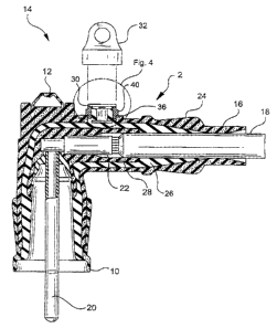
Figure 2 is a cross-sectional view o~a prior art power cable elbow connector
2, which includes a cable receiving end 16 having a cable 18 therein. The
other end
of the power cable elbow is a loadbreak bushing insert receiving end 10 having
a
probe or energized electrode 20 positioned within a central opening of the
bushing
recei~riz~g end- The probe 20 is coinnected via a cable connector 22 to the
cable 18.
The power cable elbow 2 includes an electrically conductive shield 24 fozxned
from a
conductive peroxide-cured synthetic rubber, known arid referred to in the art
as
EPDM. Within the shield .24, the power cable elbow 2 includes an insulative
inner
housing 26, typically molded from an insulative rubber or epoxy material, and
within
the insulative inner housing, the power cable elbow cozu~ector includes a
conductive
1 S insert 28 which surrounds the connection portion 22 of the cable 18.
The power cable elbow connector also includes a~x opening eye 12 for
providing hot-stick operation and a voltage detection test point 14 for
testing voltage
with appropriate voltage sezzsing devices. The voltage detection test point 14
includes
a test point terminal 30 Embedded in a portion 34 of the insulating sheath 26
that
extends tlu-ough an opening 3G within the conductive shield 24- The ternczinal
30,
which is formed of a conductive metal or plastic, is exposed exterior to the
conductive
shield 24, but is separated from the shield by the insulating portion 34
suzxounding tlae
terminal. Thus, the test point terminal 30 is capacitively coupled to the
electrical
conduetoz elements within the connector. An insulating protective cap 32
sealingly
2~ engages the portion 34 of the insulating sheath 2& that extends through the
conductive
shield 24 about the test point terminal 30 to pxatect the terminal from
environmental
conditions.
A.s previously mentioned, to minimize the chances of electrical shock, it is
izrxportant that the insulating portion 34 surrounding the terminal 30 be free
of any
surface irregularities andJor contan~znants. Also, a smooth surface on the
surrounding
insulating portion 34 ensures an air and water tight seal with the protective
cap 32.
6
CA 02454445 2003-12-30
1-Iowever, because of the nature of the material of the insulative sheath 26
and how it
is typically molded, surface irregularities and contaminants on the portion 34
surrounding the texxuinal are not uneomxnon.
Specifically, in a typical molding process, a prefonned conductive shield 24,
the uzternal conductive members and a terminal 30 are positioned within a
rubber or
epoxy mold and the insulative rubber or epoxy is injected within the shield to
form
tlxe inner insulative sheath 26. To form the voltage detectiozi test point 14,
the
terW ial 30 is held within the mold at a location adjacent the opening 36 of
the
conductive shield 24 and the insulative rubber or epoxy is allowed to flow
through the
opening to encapsulate the terminal. Thus, in the area of the portion 34
surxvunding
the terminal 30, the insulative rubber or epoxy comes into dixect contact with
the
mold. As mentioned above, this xesults in mold parting lines, flash,
coxztaminants,
voids and other irregularities being formed on the surface of the terminal
portion 34.
Refex-ring now to Figures 3-6, the present invexztion elin-zinates the
possibilities
of such disruptions being formed uxx the terr~~inal portion by providing a pre-
molded
plastic ixxsulation shield 40, which is pt-e-assembled with the terminal 30
arid, together
with the terminal, is positioned within the insulative mold adjacent the
conductive
shield opening 36 to be held by the rubber or epoxy material injected within
the
conduetz~re shield 24. Thus, the pre-molded insulation shield 40 beco~~~zes
coextensive
with the insulative sheath 26 upon molding and the rubber or epoxy material
injected
within the eonductxve shield does not cozzxe into contact with the mold
surfaces in the
area surrounding the termi~aal 30.
In a preferred embodiment, the pre-molded plastic insulation shield 40 is an
annular ring fozzned, for example, by injection molding, blow molding or spin
molding of an. insulative material, such as glass-filled nylon. The chosen
material is
also preferably a low coefficient of friction material to reduce frictional
forces
between the interface surfaces upon assembly and disassex~tbly of the
protective cap
32. Also, the shield 40 may be separately molded from a different colored
material
than that of the outer conductive shield 24 to provide an indication of the
operating
0 voltage of the coru~ector. For example, a red plastic shield may be
indicative of a
7
CA 02454445 2003-12-30
15kV loadbreak elbow connector while a blue shield rzaay be indicative of a
25kV
connector and so on.
'fhe separately molded shield ring 40 further preferably ixzcludes some form
of
structure which engages the terminal 30 in a pre~assen~.bled state. For
Example, the
stt~ucture may include a raised rib or groove 42 formed on the inner annular
surface 43
of the ring 40, which cooperates with a respective groove or rib structure 44
provided
on art outer annular surface 45 of the terminal 30 so that the terminal can be
snapped
in place withuz the insulation shield 40 in a pre-assembled state, as shown in
Figures 5
and 6.
1 C) Formation of the elbow connector is then carried out as described above.
In
particular, the interzxal conductive members 20, 22, 28 az~d the outer
conductive shield
24 are ~xst secured within a rubber or epoxy mold in their respective
positiozts. The
now pre-assembled insulation shield ring 40 atzd terminal 30 ate also
positioned
W thin the mold adjacent die opezzing 36 of the conductive shield 24. An
adhesion
1 ~ pxomoter tnay be applied to the shield ring 40 prior to moldW g to enhance
bonding
between, the shield ring and the rubber or epoxy insulative material. pace all
the
connector components are in place, the insulative material is then injected
within the
conductive shield 24 to form tile inner insulative sheath 26. The injected
insulative
material contacts the plastic material of the shield ring 40 through the
opening 36
20 funned within the conductive shield 24 to hold the insulative shield ring
in place.
Tlzus, as opposed to the injection molded rubber ox epoxy n~,aterial forzxW g
the
portion 34 surrounding the terralinal 30, the W sulation shield xing 40
provides the
critical electrical interface surfaces fox the voltage detection, test poixxt.
As used herein, the phrase "held by" can. refer to any means of securing the
25 separately molded insulative shield ring 40 and the terminal 30 in place on
the
electrical conxxector. Thus, in the preferred embodiment as shown in Figures 3-
6, the
terminal 30 is shaped to be mechanically held by the insulative n aaterial
foxzning the
sheath housing 26 upon molding. Also, as mentioned above, adhesion promoters
may
be used so that the terminal 30 azzd/or ring 40 can be chemically bonded to
the inner
30 insulative housing 26 during molding. It is also conceivable that the
terminal 30
CA 02454445 2003-12-30
and/or the plastic insulative shield 40 can be held to the izaner housing 26
with a
suitable adhesive applied after molding of the components, as shown in Figure
7.
Additionally, in an alternative embodiment, the pre-assembled shield ring 40
and terminal 30 can instead be held to the outer conductive shield 24. This
too can be
achieved by providing structure which ensuzes that the shield ring 40 and the
terminal
30 are mechanically held in place during molding, or by chemically bonding or
otherwise adhering the shield directly to the outer conductive shield 24, so
long as the
termizaal is electrically isolated from the outer conductive shield. In this
embodiment,
the opening 36 forn~ed in the outer conductive shield 24 for accommodating the
plastic shield ring 40 arid terminal 30 would no longer be required.
However, it has been found that the preferred metkzod according to the present
invention provides considerable txzanufacturing benefits. In particular, by
first
separately molding a plastic voltage detection point insulation shield 40 azzd
then
placing the shield within a housing mold, wherein a rubber or epoxy inner
housxz~g is
molded, several significant benefits can be achieved.
First, at the critical electrical interface surface on the exterior of the
insulative
portion surrounding the test point terminal 30, the rubber or epoxy housing
material
only comes into contact with the shield riuig 40, as opposed to the cavity
surfaces of
the mold. Isolating the rubber or epoxy insulatioza material frozen the mold
cavity in
this area eliminates the possibility of contaminants from the mold surfaces
being
transferred to the critical electrical interface surfaces surrounding the
voltage test
point terminal 30, which typically results in a scrapped part.
Second, the pre-molded shield ring 40 placed within th.e rubber n~.old
prevents
excess flashing arid eliminates mold parting lines at the critical electrical
interface
surfaces surrounding the voltage test point ternzixzal 30. The z-ubber or
epoxy material
typically used to rxzold the inner housing sheath 26 tends to seep freely
within the
mold during the injection zxzolding process regardless of the precision used
in
fabricating the ixzoId. Thus, once cured after molding, any areas of the
insulative
housing that come into contact with a rzxold surface must be carefully trir~az-
zred of alI
n.zbber or epoxy flash. Aside from the time consuming and labor intensive
process of
9
CA 02454445 2003-12-30
trimming the excess flash, there is also the drawback of marring or disrupting
the
surface of the housing, which could result in electrical failure at high
voltage.
Moreover. Even with the utmost care in removing the flash, mold parting lines
n~zay be
left on the housing, which may result in an electrical short. By injection n
~oldi~:ag the
rubber oz' epoxy material within the pie-formed conductive shell 24 and shield
ring
40, these dz~awbacks are eliminated since the shell and the shield ring
prevent the
IIlO1d~11~,T material from seepixtg and farming flash.
Third, minizxiizing the areas irz which the zubber or epoxy material comes
into
contact with a mold surface further ezlhances the lifetime and cleanliness of
the mold.
With conventional rubber and epoxy molding of high voltage connectors, the
injected
material comes i.n direct contact with the txzold surfaces. To prevent the
rubber or
epoxy .from sticking to the mold, release agents are often applied to the.
mold cavities.
Aside from the possibility of the release agents contaminating the finished
molded
part, these release agerafis can be abrasive and cause wear on the mold cavity
surfaces.
Moreover, despite the application of the release agent, the molded material,
which is
also abrasive, still often stinks to the mold which may result in voids or
other
irregularities being fornned on a critical surface when the housing is removed
from the
Ill~ld. These voids and irregularities must then be patched to preserve the
part.
Additionally, the rubber arid epoxy remnants, as well as the other gaseous by-
products
of the curing process, deposited on the mold surfaces require the mold to be
cleaned
regularly. The method according to the present invention zxziniznizes mold
cleaning
azid its associated costs and down time in manufacturing, as well as prolongs
the life
of the. mold, by isolating the molding material from the mold surfaces.
Finally, because of the nature of the plastic material, smoother surface
finishes
can be achieved on the exterior of the shield ring 40, as compared to rubber
or epoxy
molded surfaces. $y providing a smoother finsh on the test poizat exterior
suz~face
that interfaces with the protective cap 32, a better aiur tight and water
tight seal cm be
achieved. A strong seal prevents dirt or other contaminants from interfering
with the
test point terminal.
While the electrical connector discussed and shown in figures 1-3 is a
loadbreak elbow connector, the separately zxlolded Shield ring of the present
invention
CA 02454445 2003-12-30
can be utilized on interface surfaces of all types of electrical correctors to
improve on
the surface f1I11Sh of critical electrical ixlterface surfaces and to reduce
the frictional
forces encountered upon assembling and disassernbliztg mating conzzectors.
Thtts, the
presezzt invention has particular application on such separable electrical
cozmectors as
loadbreak connectors and deadbreak connectors. F-Iowever, the invention is not
limited to these particular embodiments. It is within the scope of the present
invention to use a low coefficient of friction ring, sleeve or other type of
structure on
any type of separable electrical connector system, wherein critical,
ele.etxical intez~face
surfaces are present and/or .frictional forces are encousltered upon assembly
and
disassenzbly.
Although the illustrative embodiments of the present invention, have beef
described herein with reference to the accompanying drawings, it is to be
understood
that the invention is not limited to those precise embodirl~.ents, and that
various othez
changes and modif-lcations znay be effected therein by one skilled in the azt
without
departing from the Scope or spirit of the invention,
11