Note: Descriptions are shown in the official language in which they were submitted.
CA 02454834 2004-O1-21
WO 03/021613 PCT/US02/23859
ELECTROMECHANICAL MEMORY ARRAY USING NANOTUBE
RIBBONS AND METHOD FOR MAKING SAME
Cross-Reference to Related Applications
This application is related to the following applications, all of which are
filed
on the same date that this application is filed, all of which are assigned to
the assignee
of this application, and all of which are incorporated by reference in their
entirety:
Hybrid Circuit Having Nanotube Electromechanical Memory (U.S. Pat. Apl.
Ser. No. not yet assigned); and
Electromechanical Memory Having Cell Selection Circuitry Constructed with
Nanotube Technology (U.S. Pat. Apl. Ser. No. not yet assigned).
Background
1. Technical Field
This invention relates in general to nonvolatile memory devices for use as
memory storage in an electronic device and in particular to nonvolatile memory
arrays
that use electromechanical elements as the individual memory cells.
2. Discussion of Related Art
Important characteristics for a memory cell in electronic device are low cost,
nonvolatility, high density, low power, and high speed. Conventional memory
solutions include Read Only Memory (ROM), Programmable Read only Memory
(PROM), Electrically Programmable Memory (EPROM), Electrically Erasable
Programmable Read Only Memory (EEPROM), Dynamic Random Access Memory
(DRAM) and Static Random Access Memory (SRAM).
ROM is relatively low cost but cannot be rewritten. PROM can be electrically
programmed but with only a single write cycle. EPROM has read cycles that are
fast
relative to ROM and PROM read cycles, but has relatively long erase times and
reliability only over a few iterative read/write cycles. EEPROM (or "Flash")
is
inexpensive, and has low power consumption but has long write cycles (ms) and
low
relative speed in comparison to DRAM or SRAM. Flash also has a finite number
of
read/write cycles leading to low long-term reliability. ROM, PROM, EPROM and
CA 02454834 2004-O1-21
WO 03/021613 PCT/US02/23859
EEPROM are all non-volatile, meaning that if power to the memory is
interrupted the
memory will retain theJinformation stored in the memory cells.
DRAM stores charge on transistor gates that act as capacitors but must be
electrically refreshed every few milliseconds complicating system design by
requiring
separate circuitry to "refresh" the memory contents before the capacitors
discharge.
SRAM does not need to be refreshed and is fast relative to DRAM, but has lower
density and is more expensive relative to DRAM. Both SRAM and DRAM are
volatile, meaning that if power to the memory is interrupted the memory will
lose the
information stored in the memory cells.
Consequently, existing technologies are either non-volatile but are not
randomly accessible and have low density, high cost, and limited ability to
allow
multiples writes with high reliability of the circuit's function, or they are
volatile and
complicate system design or have low density. Some emerging technologies have
attempted to address these shortcomings.
For example, magnetic RAM (MRAM) or ferromagnetic RAM (FRAM)
utilizes the orientation of magnetization or a ferromagnetic region to
generate a
nonvolatile memory cell. MRAM utilizes a magnetoresisitive memory element
involving the anisotropic magnetoresistance or giant magnetoresistance of
ferromagnetic materials yielding nonvolatility. Both of these types of memory
cells
have relatively high resistance and low-density. A different memory cell based
upon
magnetic tunnel junctions has also been examined but has not led to large-
scale
commercialized MRAM devices. FRAM uses a circuit architecture similar to DRAM
but which uses a thin film ferroelectric capacitor. This capacitor is
purported to retain
its electrical polarization after an externally applied electric field is
removed yielding
a nonvolatile memory. FRAM suffers from a large memory cell size, and it is
difficult to manufacture as a large-scale integrated component. See U.S.
Patent Nos.
4,853,893; 4,888,630; 5,198,994
Another technology having non-volatile memory is phase change memory.
This technology stores information via a structural phase change in thin-film
alloys
incorporating elements such as selenium or tellurium. These alloys are
purported to
remain stable in both crystalline and amorphous states allowing the formation
of a bi-
stable switch. While the nonvolatility condition is met, this technology
appears to
suffer from slow operations, difficulty of manufacture and reliability and has
not
2
CA 02454834 2004-O1-21
WO 03/021613 PCT/US02/23859
reached a state of commercialization. See U.S. Patent Nos. 3,448,302;
4,845,533;
4,876,667; 6,044,008.
Wire crossbar memory (MWCM) has also been proposed. See U.S. Patent
Nos. 6,128,214; 6,159,620; 6,198,655. These memory proposals envision
molecules
as bi-stable switches. Two wires (either a metal or semiconducting type) have
a layer
of molecules or molecule compounds sandwiched in between. Chemical assembly
and electrochemical oxidation or reduction are used to generate an "on" or
"off ' state.
This form of memory requires highly specialized wire junctions and may not
retain
non-volatility owing to the inherent instability found in redox processes.
Recently, memory devices have been proposed which use nanoscopic wires,
such as single-walled carbon nanotubes, to form crossbar junctions to serve as
memory cells. See WO 01/03208, Nanoscopic Wire-Based Devices, Arrays, and
Methods of Their Manufacture; and Thomas Rueckes et al., "Carbon Nanotube-
Based
Nonvolatile Random Access Memory for Molecular Computing," Science, vol. 289,
pp. 94-97, 7 July, 2000. Hereinafter these devices are called nanotube wire
crossbar
memories (NTWCMs). Under these proposals, individual single-walled nanotube
wires suspended over other wires define memory cells. Electrical signals are
written
to one or both wires to cause them to physically attract or repel relative to
one
another. Each physical state (i.e., attracted or repelled wires) corresponds
to an
electrical state. Repelled wires are an open circuit junction. Attracted wires
are a
closed state forming a rectified junction. When electrical power is removed
from the
junction, the wires retain their physical (and thus electrical) state thereby
forming a
non-volatile memory cell.
The NTWCM proposals to date rely on directed growth or chemical self-
assembly techniques to grow the individual nanotubes needed for the memory
cells.
These techniques are now believed to be difficult to employ at commercial
scales
using modern technology. Moreover, they may contain inherent limitations such
as
the length of the nanotubes that may be grown reliably using these techniques,
and it
may difficult to control the statistical variance of geometries of nanotube
wires so
grown.
Summary
The invention provides electromechanical circuits, such as memory cells, and
methods for making same. The circuits include a structure having electrically
CA 02454834 2004-O1-21
WO 03/021613 PCT/US02/23859
conductive traces and supports extending from a surface of the substrate, and
nanotube ribbons suspended by the supports that cross the electrically
conductive
traces, wherein each ribbon comprises one or more nanotubes.
According to one aspect of the invention, the electro-mechanical circuit
elements are made by providing a structure having electrically conductive
traces and
supports, in which the supports extend from a surface of the substrate. A
layer of
nanotubes is provided over the supports, and portions of the layer of
nanotubes are
selectively removed to form ribbons of nanotubes that cross the electrically
conductive traces. Each ribbon includes one or more nanotubes.
Brief Description of the Drawing
In the Drawing,
Figure 1 illustrates a nanotube belt crossbar memory device according to
certain embodiments of the invention;
Figures 2A-B illustrate two states of a memory cell according to certain
embodiments of the invention;
Figure 3 illustrates acts of making memory devices according to certain
embodiments of the invention;
Figures 4-11 illustrate several forms of creating an intermediate structure
used
to make memory devices according to certain embodiments of the
invention;
Figure 12 illustrates the non-woven nanotube fabric, or matted nanotube layer,
used to make certain embodiments of the invention;
Figure 13 illustrates the matted nanotube layer in relation to hidden,
underlying traces of certain embodiments of the invention;
Figure 14 illustrates addressing logic of certain embodiments of the
invention;
Figure 15 illustrates a hybrid technology embodiment of the invention in
which the memory core uses nanotube technology; and
Figure 16 illustrates a hybrid technology embodiment of the invention in
which the memory core and addressing lines use nanotube ribbon
technology.
Detailed Description
Preferred embodiments of the invention provide new electromechanical
memory arrays and methods for making same. In particular, electromechanical
4
CA 02454834 2004-O1-21
WO 03/021613 PCT/US02/23859
memory cells are created that operate anaologously to the NTWCM devices
disclosed
in WO Ol /03208, which is hereby incorporated by reference in its entirety.
However,
unlike the NTWCM devices disclosed in WO 01/03208, preferred embodiments of
the
invention replace
the suspended nanoscopic wires used in the NTWCM devices with new ribbons made
from a matted layer of nanotubes or a non-woven fabric of nanotubes. These new
devices are referred to herein as nanotube ribbon crossbar memories (NTRCMs).
The
new nanotube belt structures are believed to be easier to build at the desired
levels of
integration and scale (in number of devices made) and the geometries are more
easily
controlled.
Because the new nanotube belt crossbar memory devices operate analogously
to NTWCM, the description of their architecture and principles of operation is
brief.
Reference may be made to WO 01/03208 for fuller description and background.
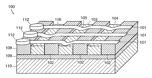
Figure 1 illustrates an exemplary electromechanical memory array 100
constructed according to principles of preferred embodiments of the invention.
The array has a plurality of non volatile memory cells 103 which can be in an
"on"
state 105 or "ofp' state 106. The actual number of such cells is immaterial to
understanding the invention but the technology may support devices having
information storage capacities equivalent to or larger than modern non-
volatile circuit
devices.
Each memory cell 103 includes a nanotube ribbon 101 suspended by one or
more supports 102 over electrical traces or wires, e.g., 104.
Each crossing of a ribbon 101 and a wire, e.g., 104 forms a crossbar junction
and defines a memory cell. Under certain embodiments, each cell may be read or
written by applying currents and or voltages to electrodes 112 which are in
electrical
communication with ribbons 101 or through electrodes (not shown) in
communication
with traces or wires 104. The supports 102 are made from a layer 108 of
silicon
nitride (Si3N4). Below layer 108 is a gate oxide layer 109 separating the n-
doped
silicon traces 104 from an underlying silicon wafer 110.
Referring conjointly to figures 1-2B, junction 106 illustrates the cell in a
first
physical and electrical state in which the nanotube ribbon 101 is separated
from
corresponding trace 104. Junction 105 illustrates the cell in a second
physical and
electrical state in which the nanotube ribbon 101 is deflected toward
corresponding
trace 104. In the first state, the junction is an open circuit, which may be
sensed as
CA 02454834 2004-O1-21
WO 03/021613 PCT/US02/23859
such on either the ribbon 1 O1 or trace 104 when so addressed. In the second
state, the
junction is a rectified junction (e.g., Schottky or PN), which may be sensed
as such on
either the tube 101 or trace 104 when so addressed.
Under certain embodiments, the nanotube ribbon 101 may be held in position
at the supports by friction. In other embodiments the ribbon may be held by
other
means, such as by anchoring the ribbons to the supports using any of a variety
of
techniques. This friction can be increased through the use of chemical
interactions
including covalent bonding through the use of carbon compounds such as pyrenes
or
other chemically reactive species. Evaporated or spin-coated material such as
metals,
semiconductors or insulators especially silicon, titanium, silicon oxide or
polyimide
could also be added to increase the pinning strength. The nanotube ribbons or
individual nanotubes can also be pinned through the use wafer bonding to the
surface.
See R.J. Chen et al., "Noncovalent Sidewall Functionalization of Single-Walled
Carbon Nanotubes for Protein Immobiliation," J.Am. Chem. Soc., 123, 2001, 3838-
39
and Dai et al., Appl. Phys. Lett., 77, 2000, 3015-17 for exemplary techniques
for
pinning and coating nanotubes by metals. See also WO01/03208 for techniques.
Under certain preferred embodiments as shown in figures 2A-B, a nanotube
ribbon 101 has a width of about 180 nm and is pinned to a support 102
preferably
fabricated of silicon nitride. The local area of trace 104 under ribbon 101
forms an n-
doped silicon electrode and is positioned close to the supports 102 and
preferably is
no wider than the belt, e.g., 180 nm. The relative separation 208 from the top
of the
support 102 to the deflected position where the belt 101 attaches to electrode
206 see
figure 2B) should be approximately 5-50 nm. The magnitude of the separation
208 is
designed to be compatible with electromechanical switching capabilities of the
memory device. For this embodiment, the S-50 nm separation is preferred for
certain
embodiments utilizing ribbons 101 made from carbon nanotubes, but other
separations may be preferable for other materials. This magnitude arises from
the
interplay between strain energy and adhesion energy of the deflected
nanotubes.
These feature sizes are suggested in view of modern manufacturing techniques.
Other
embodiments may be made with much smaller (or larger) sizes to reflect the
manufacturing equipment's capabilities.
The nanotube ribbon 101 of certain embodiments is formed from a non-woven
fabric of entangled or matted nanotubes (more below). The switching parameters
of
the ribbon resemble those of individual nanotubes. Thus, the predicted
switching
6
CA 02454834 2004-O1-21
WO 03/021613 PCT/US02/23859
times and voltages of the ribbon should approximate the same times and
voltages of
nanotubes. Unlike the prior art which relies on directed growth or chemical
self-
assembly of individual nanotubes, preferred embodiments of the present
invention
utilize fabrication techniques involving thin films and lithography. This
method of
fabrication lends itself to generation over large surfaces especially wafers
of at least
six inches. (In contrast, growing individual nanotubes over a distance beyond
sub
millimeter distances is currently unfeasible.) The ribbons should exhibit
improved
fault tolerances over individual nanotubes, by providing redundancy of
conduction
pathways contained with the ribbons. (If an individual nanotube breaks other
tubes
within the rib provide conductive paths, whereas if a sole nanotube were used
the cell
would be faulty.) Moreover, the resistances of the ribbons should be
significantly
lower than that for an individual nanotubes, thus, decreasing its impedance,
since the
ribbons may be made to have larger cross-sectional areas than individual
nanotubes.
Figure 3 illustrates a method of making certain embodiments of NTRCM
devices 100. A first intermediate structure 302 is created or provided. In the
illustrated embodiment, the structure 302 includes a silicon substrate 110
having an
insulating layer 109 (such as silicon dioxide) and a silicon nitride layer
(Si3N4 ) 108
that defines a plurality of supports 102. In this instance, the supports 102
are formed
by rows of patterned silicon nitride, though many other arrangements are
possible,
such as a plurality of columns. Conductive traces 104 extend between supports
102.
In this instance, the traces 104 are shown as essentially contacting the
supports 102,
but other arrangements are possible as are other geometries; for example,
spaces may
exist between trace 104 and support 102 and trace 104 may be fashioned as a
wire or
may have non-rectangular transverse, cross-sections, including triangular or
trapezoidal. Sacrificial layers 304 are disposed above the traces 104 so as to
define
one planar surface 306 with the upper surface of the supports 102. This planar
surface, as will be explained below, facilitates growth of a matted nanotube
layer of
certain embodiments.
Once such a structure 302 is created or provided, the upper surface 306
receives a catalyst 308. For example, under certain embodiments, a catalyst
metal
308, containing iron (Fe), molybdenum (Mo), cobalt or other metals, is applied
by
spin-coating or other application techniques to create a second intermediate
structure
310.
7
CA 02454834 2004-O1-21
WO 03/021613 PCT/US02/23859
A matted layer 312 of nanotubes is then grown into a non-woven fabric of
single-walled carbon nanotubes (SWNTs) to form a third intermediate structure
314.
For example, the second intermediate structure 310 may be placed into an oven
and
heated to a high temperature (for example, about 800-1200°C) while
gases containing
a carbon source, hydrogen and inert gas, such as argon or nitrogen, are flowed
over
the upper surface. This environment facilitates the generation or growth of
the matted
layer or film 312 of single-walled carbon nanotubes. The layer 312 is
primarily one
nanotube thick and the various tubes adhere to one another via Van der Waals
forces.
Occasionally, one nanotube grows over the top of another, though this growth
is
relatively infrequent due to the growth tendencies of the material. Under some
embodiments (not shown), the catalyst 308 may be patterned to assist in
growing the
nanotubes with specific densities either more or less dense as is desired.
When
conditions of catalyst composition and density, growth environment, and time
are
properly controlled, nanotubes can be made to evenly distribute over a given
field that
is primarily a monolayer of nanotubes. Proper growth requires control of
parameters
including but not limited to catalyst composition and concentration,
functionialization
of the underlying surface, spin coating parameters (length and RPM), growth
time,
temperature and gas concentrations.
A photoresist may then be applied to the layer 312 and patterned to define
ribbons in the matted layer of nanotubes 312. The ribbon patterns cross (for
example,
perpendicularly) the underlying traces 104. The photoresist is removed to
leave
ribbons 101 of non-woven nanotube fabric lying on planar surface 306 to form
fourth
intermediate structure 318.
The fourth intermediate structure 318 has portions 320 of its underlying
sacrificial layer 304 exposed as shown. The structure 318 is then treated with
an acid,
such as HF, to remove the sacrificial layer 304, including the portion under
the
ribbons 101, thus forming an array 322 of ribbons 101 suspended over traces
104 and
supported by supports 102.
Subsequent metalization may be used to form addressing electrodes, e.g., 112
shown in figure 1.
One aspect of the above technique is that the various growth, patterning, and
etching operations may use conventional techniques, such as lithographic
patterning.
Currently, this may entail feature sizes (e.g., width of ribbon 101) of about
180 nm to
8
CA 02454834 2004-O1-21
WO 03/021613 PCT/US02/23859
as low as 130 mm, but the physical characteristics of the components are
amenable to
even smaller feature sizes if manufacturing capabilities permit.
As will be explained below, there are many possible ways of creating the
intermediate structures or analogous structures described above. Figure 4, for
example, shows one way to create the first intermediate structure 302
A silicon wafer 400 is provided with an oxide layer 402. The oxide layer is
preferably a few manometers in thickness but could be as much 1 p.m. A silicon
nitride
(Si3N4) layer 404 is deposited on top of the oxide surface 402. The silicon
nitride
layer is preferably at least 30 mm thick.
The silicon nitride layer 404 is then patterned and etched to generate
cavities
406 to form support structure 407. With modern techniques the cavity width may
be
about 180 mm wide or perhaps smaller. The remaining silicon nitride material
defines
the supports 102 (e.g., as row, or perhaps columns).
A covering 408 of n-doped silicon is then deposited to fill the cavities 406.
The covering 408 for exemplary embodiments may be about 1 pm thick but may be
as
thin as 30 mm.
The covering 408 is then processed, for example by self-flattening of thick
silicon layers or by annealing, to produce a planar surface 306, discussed
above, to
form structure 411. In the case of self-flattening, reactive ion-etching (RIE)
with
end-point detection (EPD) may be utilized until the upper surface 410 of the
etched
silicon nitride is reached.
The structure 411 is then oxidized to form and define sacrificial layers 304
of
SiOz about 10-20 mm deep into planar surface 306.
The unconverted, remaining portions of silicon form traces 104.
Figure 5 shows another method that may be used to create the NTRCM
devices 100 of certain embodiments. A support structure 407, like that
described in
connection with figure 4, is provided. A layer 514 of n-doped silicon is then
added
using a CVD process, sputtering or electroplating. Under certain embodiments,
layer
514 is added to be about half the height of the Si3N4 supports 102.
After the layer 514 is added, an annealing step is performed to yield a
planarized surface 306 to form a structure 411 like that described above. The
annealing step causes the silicon of layer 514 to flow into the cavities 406.
9
CA 02454834 2004-O1-21
WO 03/021613 PCT/US02/23859
Like that described in connection with figure 4, the structure 411 is then
oxidized to form and define sacrificial layers 304 of SiOz about 10-20 nm deep
into
planar surface 306.
Figure 6 shows another approach for forming an alternative first intermediate
structure 302'. In this embodiment, a silicon substrate 600 is covered with a
layer 602
of silicon nitride having a height 604 of at least 30 nm.
The silicon nitride layer 602 is then patterned and etched to generate
spacings
606 and to defined supports 102. The etching process exposes a portion 608 of
the
surface of silicon substrate 600.
The exposed silicon surface 608 is oxidized to generate a silicon dioxide
(Si02) layers 610 having a thickness of a few nm. These layers 610 eventually
insulate traces 104 analogously to the way insulating layer 109 did for the
above
described structures 302.
Once the insulating layers 610 have been created, the traces 104 may be
created in any of a variety of manner. Figure 6 illustrates the processing
steps of
figures 4-S used to create such traces to illustrate this point.
Figure 7 shows another approach for forming first intermediate structure 302.
A silicon substrate 700 having a silicon dioxide layer 702 and a silicon
nitride layer
704 receives a patterned photoresist layer 706. For example, a photoresist
layer may
be spin-coated on layer 704 and subsequently exposed and lithographically
developed.
Reactive ion etching (RIE) or the like may then be used to etch the Si3N41ayer
704 to form cavities 708 and to define supports 102.
Afterwards, n-doped silicon 710 may be deposited in the cavities 708. Under
certain embodiments silicon is deposited to a height about equal to the height
712 of
the Si3N4 supports 102.
The photoresist 706 and silicon 710 on top of the photoresist 706 are then
stripped away to form an intermediate structure 411 like that described above.
The structure 411 is then oxidized to generate the sacrificial Si02 layers
304.
Figure 8 shows another approach for forming first intermediate structure 302.
Under this approach, a starting structure 800 is provided having a lowest
silicon layer
802 with a lowest silicon dioxide layer 804 on top of it. A second silicon
layer 806 is
on top of layer 804 and a second silicon dioxide layer 808 is on top of the
second
silicon layer 806.
CA 02454834 2004-O1-21
WO 03/021613 PCT/US02/23859
The top silicon dioxide (Si02) layer 808 is patterned by photolithography to
create an RIE mask 810. The mask is used to etch the exposed portions 812 of
second
silicon layer 806 down to the first silicon dioxide layer 804. This etching
creates
cavities 814 and defines traces 104.
The cavities 814 are filled and covered with silicon nitride (Si3N4) 816.
The Si3N4 covering 816 is backetched with RIE to the same height 818 as the
remaining portions of the Si02 layer 806 covering the n-doped silicon
electrodes 104
(which form the sacrificial layer 304).
Figure 9 shows an approach for forming an alternative first intermediate
structure 302". Under this approach, a structure like 407 (shown in figure 4,
but not
figure 9) is provided. In this instance, the Si3N4 supports 102 have a height
of about
30 nm. A thin layer of metal 902 is deposited on top of the Si3N4 supports 102
and on
top of the exposed portions Si02 at the bottom of the cavities 904 as depicted
by item
903. Metal 902 and 903 form temporary electrodes. A layer of n-doped silicon
906
may then be deposited or grown by electroplating, covering the electrode 903
until the
silicon 906 achieves a height 908 at the top of the support 102 and contacting
electrode 902. The growth process may be controlled by the onset of a current
flow
between the lower and upper metal electrodes 902,3.
The exposed metal electrodes 902 may then be removed by wet chemical
methods or dry chemical methods. This forms an intermediate structure 411'
like the
structure 411 described above, but with a buried electrode 903, as an artifact
of the
silicon growing process.
The structure 411' is then oxidized to form sacrificial layers 304 at the
exposed portions of silicon, as described above. For example, the layers 304
may be
grown to a thickness of about 10 nm.
Figure 10 shows another approach for forming first intermediate structure 302.
A silicon substrate 1002 having a layer of silicon dioxide 1004 on top of it
and a
second layer 1006 of silicon (n-doped) on top of layer 1004 is used as a
starting
material. A mask layer 1008 is photolithographically patterned on top of layer
1006.
Using nitridization techniques, exposed portions 1010 of n-doped silicon layer
1006 are chemically converted to Si3N4 supports 102. The unconverted portions
of
layer 1006 form traces 104.
The mask 1008 is removed forming a structure 411 like that described above.
11
CA 02454834 2004-O1-21
WO 03/021613 PCT/US02/23859
The exposed portions 1012 of silicon surface are then oxidized to form the
Si02 sacrificial layers 304.
Figure 11 shows an approach for forming an alternative first intermediate
structure 302"' Under this approach a silicon substrate 1102 is layered with a
thin
film 1104 of Si3N4 as a starting structure. On top of the silicon nitride
layer 1104, n-
doped silicon is added and lithographically patterned, by RIE, to form traces
104.
The surfaces of traces 104 are oxidized to form the Si02 layer 1106 which acts
as an alternative form of sacrificial layer 304'.
The structure is overgrown with Si3N41108 and back etched to form a planar
surface 306 and to form alternative first intermediate structure 302"'. As
will be
evident to those skilled in the art, under this approach, when the sacrificial
layer is
subsequently removed, traces 104 will be separated from supports 102. Other
variations of this technique may be employed to create alternative transverse
cross-
sections of trace 104. For example, the traces 104 may be created to have a
rounded
top, or to have a triangular or trapezoidal cross section. In addition, the
cross section
may have other forms, such as a triangle with tapered sides.
As was explained above, once a first intermediate structure is formed, e.g.,
302, a matted nanotube layer 312 is provided over the planar surface 306 of
the
structure 302. In preferred embodiments, the non-woven fabric layer 312 is
grown
over the structure through the use of a catalyst 308 and through the control
of a
growth environment. Other embodiments may provide the matted nanotube layer
312
separately and apply it directly over the structure 302. Though structure 302
under
this approach preferably includes the sacrificial layer to provide a planar
surface to
receive the independently grown fabric, the sacrificial layer may not be
necessary
under such an approach.
Because the growth process causes the underside of such nanotubes to be in
contact with planar surface 306 of intermediate structure 302, they exhibit a
"self-
assembly" trait as is suggested by figure 12. In particular, individual
nanotubes tend
to adhere to the surface on which they are grown whenever energetically
favorable,
such that they form substantially as a "monolayer." Some nanotubes may grow
over
another so the monolayer is not expected to be perfect. The individual
nanotubes do
not "weave" with one another but do adhere with one another as a consequence
of
Van der Waals forces. Figure 12 is an approximate depiction of an actual
nanotube
non-woven fabric. Because of the small feature sizes of nanotube, even modern
12
CA 02454834 2004-O1-21
WO 03/021613 PCT/US02/23859
scanning electron microscopy cannot "photograph" an actual fabric without loss
of
precision; nanotubes have feature sizes as small as 1-2nm which is below the
precision of SEM. Figure 12 for example, suggests the fabric's matted nature;
not
clear from the figure, however, is that the fabric may have small areas of
discontinuity
with no tubes present. Each tube typically has a diameter 1-2 nm (thus
defining a
fabric layer about 1-2 nm) but may have lengths of a few microns but may be as
long
as 200 microns. The tubes may curve and occasionally cross one another. Tubes
attach to one another via Van der Waals forces.
In certain embodiments, nanotubes grow substantially unrestrained in the x-
and y-axis directions, but are substantially restricted in the z-axis
(perpendicular to
page of figure 12) as a consequence of the self-assembly trait. Other
embodiments
may supplement the above approach to growing matte 312 with the use of field-
oriented or flow-oriented growth techniques. Such supplementation may be used
to
further tailor growth such that any growth in one planar axis (e.g. the -x-
axis) is
retarded. This allows for a more even coverage of the desired area with a
planar
interwoven monolayer coating of nanotubes with a controllable density.
A plan view of the matted nanotube layer 312 with underlying silicon traces
104 is shown in figure 13.
As explained above, once the matted nanotube layer 312 is provided over the
surface 306, the layer 312 is patterned and etched to define ribbons 101 of
nanotube
fabric that cross the supports 102. The sacrificial layer is then removed
(e.g., with
acid) forming the array 322 described above in connection with figure 3.
Because the
matted layer of nanotubes 3l2 form a non-woven fabric that is not a contiguous
film,
etchants or other chemicals may diffuse between the individual nanotube
"fibers" and
more easily reach the underlying components, such as the sacrificial layer.
Subsequent metalization may be used to form addressing electrodes, e.g., 112
shown in figure 1, as outlined above. Other embodiments use nanotube
technology to
implement addressing of memory cells instead of using metallized electrodes
112 and
addressing lines (not shown).
More specifically, under certain embodiments described above, nanotubes are
used to form NTRCM arrays. Certain embodiments use nanotube technology,
whether in individual wire or belt form, to implement addressing logic to
select the
memory cells) for reading or writing operations. This approach furthers the
integration of nanotube technology into system design and may provide
beneficial
13
CA 02454834 2004-O1-21
WO 03/021613 PCT/US02/23859
functionality to higher-level system design. For example, under this approach
the
memory architecture will not only store memory contents in non-volatile manner
but
will inherently store the last memory address.
The nanotube-based memory cells have bistability characterized by a high
ratio of resistance between "0" and "1" states. Switching between these states
is
accomplished by the application of specific voltages across the nanotube belt
or wire
and the underlying trace, in which at least one of the memory cell elements is
a
nanotube or a nanotube ribbon. In one approach, a "readout current" is applied
and
the voltage across this junction is determined with a "sense amplifier." Reads
are
non-destructive, meaning that the cell retains its state, and no write-back
operations
are needed as is done with DRAM.
Figure 14 depicts a branching binary select system, or decoder, 1400. As will
be explained below, decoder 1400 may be implemented with nanotubes or nanotube
ribbon technology. Moreover, the decoder may be constructed on the same
circuit
component as a nanotube memory cell array, e.g., NTRCM or NTWCM.
A perpendicular intersection of two lines 1404 and 1406 depicted as a dot
1402 indicates a junction of two nanotubes or nanotube ribbons. In this
regard, the
interaction is analogous to a "pass transistor" found in CMOS and other
technology,
in which the intersection may be opened or closed.
Locations such as 1420 where one nanotube or nanotube ribbon may cross
another but which are not intended to create a crossbar junction may be
insulated from
one another with a lithographically patterned insulator between the
components.
For the sake of clarity, the decoder illustrated is for a 3-bit binary address
carried on addressing lines 1408. Depending on the value of the encoding the
intersections (dots) will be switched to create only one path through which
sensing
current I may pass to select lines 1418.
To use this technique, a "dual rail" representation 1408 of each bit of the
binary address is fashioned externally so that each of the address bits 1410
is
presented in true and complementary form. Thus, line 1406 may be the logical
true
version of address line 1408a and line 1407 may be the logical complement of
address
line 1408a. The voltage values of the representation 1408 are consistent with
that
needed to switch a crossbar junction to the "1" or "0" state as described
above.
In this fashion an address 1408 may be used to supply a sense current I to a
bit
or row of bits in an array, e.g., to nanotubes or nanotube ribbons. Likewise,
the same
14
CA 02454834 2004-O1-21
WO 03/021613 PCT/US02/23859
approach may be used to sense a given trace, for example, selecting specific
array
columns) to read sense from in conjunction with selecting a row. Thus this
approach
may be used for X and/or Y decoding both for reading and for writing
operations.
Certain embodiments of the invention provide a hybrid technology circuit
1500, shown in figure 15. A core memory cell array 1502 is constructed using
NTWCM or NTRCM, and that core is surrounded by semiconductor circuits forming
X and Y address decoders 1504 and 1506; X and Y buffers 1508 and 1510; control
logic 1512 and output buffers 1514. The circuitry surrounding the NTWCM or
NWBCM core may be used for conventional interfacing functions, including
providing read currents and sensing output voltages.
In other embodiments, the X and Y address decoders 1504 and 1506 may be
substituted with the nanotube wire or belt addressing technique discussed
above. In
these embodiments the core would include memory cells and addressing logic.
In certain embodiments, the hybrid circuit 1500 may be formed by using a
nanotube core (having either just memory cells or memory cells and addressing
logic)
and by implementing the surrounding circuitry using a field programmable gate
array.
The core and gate array circuitry may be contained in a single physical
package if
desired. Or, they may be packaged separately. For example, a hermetically
packaged
nanotube circuit (having memory or memory and addressing logic) may be
combined
with a PLD/FPGA/ASIC in which the I/O interfacing logic is contained. The
resulting
compact chipset provides access to the benefits of the NT memory for the user
of the
product, while maximizing the use of "off-the-shelp' technologies, which may
be
utilized on an as-needed basis by the manufacturer.
Figure 16 depicts one possible implementation 1600 of the hybrid technology.
A FPGA chip 1602 containing the buffering and control logic (described above)
is
connected via conducting traces on a (perhaps multilayer) printed circuit
board (PCB)
1604 to a nanotube (NT) chip 1606 containing the memory cells and addressing
logic.
This particular embodiment is suggested to conform to the PCI bus standard,
typical of today's personal computers. Other passive circuitry, such as
capacitors,
resistors, transformers, etc. (not pictured) would also be necessary to
conform to the
PCI standard. A front-side bus speed of 200MHz - 400 MHz is annotated,
suggesting
the kinds of external clock speeds such a chipset might run at. This speed is
limited by
the PCB interconnects and FPGA/PLD/ASIC speed, and also the chip packages, not
the NT memory cell speed.
CA 02454834 2004-O1-21
WO 03/021613 PCT/US02/23859
Other Embodiments
Besides carbon nanotubes other materials with electronic and mechanical
properties suitable for electromechanical switching could be envisioned. These
materials would have properties similar to carbon nanotubes but with different
and
likely reduced tensile strength. The tensile strain and adhesion energies of
the
material must fall within a range to allow bistability of the junction and
electromechanical switching properties to exist within acceptable tolerances.
For the purpose of integrating CMOS logic for addressing two approaches can
be envisioned. In the first embodiment the nanotube array will be integrated
before
metallization but after ion implantation and planarization of the CMOS logic
devices.
A second method involves growth of the nanotube arrays before fabrication of
the
CMOS devices involving ion implementation and high temperature annealing
steps.
Upon completion of these steps the final metallization of both the nanotube
ribbons
and the CMOS devices will proceed using standard and widely used protocols.
Electrodes consisting of n-doped silicon on top of some metal or
semiconductor line can also be envisioned. This will still provide rectifying
junctions
in the ON state so that no multiple current pathways exist.
In addition to rectifying junctions, there are other widely accepted and used
methods to prevent the occurrence of electrical crosstalk (i.e. multiple
current
pathways) in crossbar arrays. Tunnel barriers on top of the static,
lithographically
fabricated electrodes prevent the formation of ohmic ON states. No leakage
currents
at zero bias voltage will occur but a small bias voltage has to be applied for
the charge
carriers to overcome this barrier and tunnel between the crossing lines.
Methods to increase the adhesion energies through the use of ionic, covalent
or other forces can be envisioned to alter the interactions with the electrode
surfaces.
These methods can be used to extend the range of bistability with these
junctions.
Nanotubes can be functionalized with planar conjugated hydrocarbons such as
pyrenes which may then aid in enhancing the internal adhesion between
nanotubes
within the ribbons.
Certain of the above aspects, such as the hybrid circuits and the nanotube
technology for addressing, are applicable to individual nanotubes (e.g., using
directed
growth techniques, etc.) or to nanotube ribbons.
It will be further appreciated that the scope of the present invention is not
limited to the above-described embodiments but rather is defined by the
appended
16
CA 02454834 2004-O1-21
WO 03/021613 PCT/US02/23859
claims, and that these claims will encompass modifications of and improvements
to
what has been described.
17