Note: Descriptions are shown in the official language in which they were submitted.
CA 02455276 2004-O1-16
1
PHYSICAL LAYERS
Field of the Invention
This invention relates to network computing systems, and particularly to the
physical
1. 5 layer of the hierarchy in a network computing system.
Background of the Invention
It is the nature of the computer system development industry to require an
exponential
performance advantage over the generations while maintaining or decreasing
system
1. 10 costs. In particular, telecommunications and networking computing
systems
additionally benefit from a reduction in the board size and an increase in
system
capabilities.
Computer system processors and peripherals continually benefit from the
1. 15 aforementioned generational performance advantage. This phenomenon is
driven by
improvements in process technology. In order to realize a proportional system
wide
improvement in performance, the connection fabric must improve along with the
improvements in processors and peripherals.
1. 20 A hierarchy of shared buses is a common fabric structure. Levels of
performance
required for the multiple devices in the system typically differentiate this
hierarchy. A
given bus is associated with one such level. Bus bridges connect the buses. In
this
structure a low performance device does not burden a high performance device.
1. 25 This type of structure benefits from an increase in bus frequency, a
wider interface,
pipelined transactions and out of order completion capability. However, these
techniques are well known, and are exploited to their full potential. Further
increases
in bus width will reduce maximum bus frequency due to skew effects i.e. as the
data-
path is altered to include a greater number of data bits, the skew, between
those
CA 02455276 2004-O1-16
2
individual bits, originating in the transmission medium, becomes increasingly
severe.
A wider bus will also increase pin count. This will affect cost, and limit the
interfaces
on a device.
1. 5 Furthermore, the maximization of bus frequency and width is incompatible
with a
many-device connection. Finally, it would be advantageous to increase the
number of
devices capable of direct communication.
Therefore, point to point, packet switched, fabric architectures have emerged
as an
1. 10 alternative to the aforementioned bus structures. Such an architecture
is beneficial in
network equipment, storage subsystems and computing platforms. Networks of
this
architecture transmit encapsulated address, control and data packets from the
source
ports across a series of routing switches or gateways to addressed
destinations. The
switches and gateways of the switching fabric are capable of determining from
the
1. 15 address and control contents of a packet, what activities must be
performed. The
architecture is capable of providing an interface for processors, memory
modules and
memory mapped I/O devices.
In a typical packet switched interconnect, the functionality is organized into
a
1. 20 hierarchy of multiple layers. The disposition of typical layers
apportions the functions
most related to control and compatibility to the highest layers. The most
rudimentary
and device oriented considerations are apportioned to the lowest layer. The
physical
layer is the lowest or most physically fundamental layer.
1. 25 Physical layer specifications define the interface between devices
including packet
transport mechanisms, flow control, and electrical characteristics.
For a packet switching network to be highly efficient, the physical layer of
the
network must strive to meet certain criteria, and for functions of the
physical layer to
1. 30 be efficiently carned out.
CA 02455276 2004-O1-16
3
Specifically:
The transmitter and receiver must establish the data integrity of the channel,
and
ideally should do so without additional hardware or cumbersome handshaking.
1. 5
The physical layer should incorporate boundary scan testing in a manner that
does not
unnecessarily skew time sensitive signals i.e. clocks.
Should the physical layer incorporate delay lines, no significant fitter
should be
1. 10 introduced due to variances in the manufacturing process.
Should the network define words that are multiple bytes in length, any
corresponding
word or byte frame signals, ideally do not require handshaking or additional
pin count
for synchronization.
1. 15
Should a physical layer receive clock incorporate multiple delay lock loops
(DLLs)
for synchronizing with a transmit clock, it should be possible to allow
adjustments of
a fraction of the finest delay lock loop.
1. 20 The problem with addressing these issues with 0.13pm CMOS is that the
power
supply voltage is 1.2V and this creates a real problem for the non logic
designer as
most of the techniques used in 3.3V or even 2.5V such as cascoding current
sources
(to improve output impedance and gain of circuits) either do not work well (or
do not
work at all).
1. 25
In many kinds of circuits, there is a fundamental set of contradictory
requirements:
high speed operation, rail to rail inputs and or outputs, and low voltage
operation.
Some examples of these are: DLLs, PLLs, charge pumps, op amps, IO pads. In all
these cases, the biasing is done with current sources and circuit performance
is often
1. 30 limited by these current sources.
CA 02455276 2004-O1-16
There is a need for improvements in the physical layer of a packet switched
fabric, to
address these concerns, in order to ensure that the fabric is highly
efficient. In
particular there is a need for increased co-ordination and synchronization
between
transmission and reception interfaces while maintaining a minimum increase in
pin
1. . S count, clock skew, and cycle overhead.
In particular, at 0.13um, the power supply voltage is 1.2 V. This present a
real
problem for a designer of circuits that are not logic circuits because typical
techniques
used in 3.3 V or even 2.5 V domains either do not work well or do not work at
all.
1. 10 For example cascading current sources to improve output impedance and
gain
circuits. Part of the problem is that in many kinds of circuits there are
fundamentally
contradictory requirements, such as high speed operation, rail-to-rail inputs
andJor
outputs, and low voltage operation. For example, these circuits include delay
lock
loops (DLL), phase lock loops (PLL), charge pumps, operational amplifiers (Op
1. 15 Amps), input/output (I!0) pads.
Summary of the Invention
This invention addresses the need for improvement in the physical layer of a
packet
switched fabric communication system such that the fabric is highly efficient.
A packet
switched fabric communication system has a switch, communications medium and a
1. 20 number of end points. The switch and end points incorporate ports. In
network
hierarchy, the physical layer is responsible for packet delivery; Improvements
to
operation of ports falls within improvements to the physical layer.
The improvements can be better understood by enumerating the advantages and
1. 25 embodiments:
It is an advantage of the present invention to overcome the need for
handshaking or
additional pin counts used in testing the transmission data integrity of a
bus. This first
advantage derives from an apparatus for testing the integrity of a data
message. This
1. 30 apparatus is an alternative to a handshaking routine or the use of a
circuit that employs
dedicated bus signals.
CA 02455276 2004-O1-16
In a high-speed data bus system, maximum performance requires the skew of each
bit
of the data line to be adjusted to optimize the moment of the transmission
cycle in
which data sampling occurs. In order to achieve this optimization, the bus is
'trained'.
1. S As a pre-amble to operation, the delay associated with each line is
varied and tested
iteratively until the best possible delay is found. It is necessary to test
the performance
of this high-speed bus and identify errors.
In a corresponding embodiment, a physical layer is disclosed including:
1. 10 a transmitter incorporating one pseudo-random bit-stream generator for
generating test
vectors, a receiver incorporating a second pseudo-random bit-stream generator
and a
comparator; where the receiver uses the comparator to compare received test
vectors to
locally generated test vectors.
1. 15 It is an advantage of the present invention to incorporate a test
circuit that does not
introduce further skew into critical clock signals. In the art, boundary scan
signals are
multiplexed with system signals in order to test integrated devices. However
direct
incorporation of scan signals into a clock multiplexed node may unnecessarily
load the
clock, creating a skew.
1. 20
In a corresponding embodiment a multiplexing circuit is disclosed having:
two tiers multiplexing, the first tier multiplexing a boundary scan signal
with a set of
clock grouped signals, the second tier selecting a first tier output on the
basis of the
clock.
1. 25
It is an advantage of the present invention to incorporate DLL delay lines in
the
physical layer, while introducing no significant fitter due to variances in
the
manufacturing process. Manufacturing variances between n and p type
transistors may
cause unbalanced pullup and pulldown behavior in a bias circuit that
ultimately results
1. 30 in DLL fitter.
CA 02455276 2004-O1-16
6
We introduce a device to adjust the current as a function of process, voltage
and
temperature. The device is a current bleeder.
In a corresponding embodiment a physical layer segment is disclosed including
a delay
line generator comprising: a voltage control input, independent positive and
negative
1. 5 bias generators with dedicated positive and negative bandgap references,
wherein each
of the generators is complementarily responsive to variances in the properties
of
internal n and p type transistors.
The nature of the improvements involves superior co-ordination,
synchronization while
1. 10 maintaining a minimum increase in pin count, clock skew, and cycle
overhead.
Brief Description of the Drawings
Fig. 1 is a block diagram of a system of the prior art.
Fig. 2 is a block diagram of a system of the prior art.
1. 15 Fig. 3 is a block diagam of an endpoint of the prior art.
Fig. 4 is a block diagram of a network hierarchy of the prior art.
Fig. S is a block diagram of a handshaking system of the prior art.
Fig. 6 is a timing diagram of a handshaking system of the prior art.
Fig. 7 is a block diagram of a co-ordination system.
1. 20 Fig. 8 is a block diagram of a transmitter.
Fig. 9 is a block diagram of a Pseudo Random Bit Stream Generator.
Fig. 10 is a block diagram of a receiver.
Fig. 11 is a multiplexing circuit according to the prior art.
Fig. 12 is a multiplexing circuit.
1. 25 Fig. 13 is a block diagram of a DLL of the prior art.
Fig. 14 is a diagram of bias circuits and delay lines according to the prior
art.
Fig. 15 is a block diagram of a DLL.
Fig. 16 is a diagram of bias circuits and delay.
Fig. 17 illustrates the current bleeder device of Fig. 16; and
1. 30 Fig. 18 illustrates an implementation of the circuit of Figs. 16 and 17.
CA 02455276 2004-O1-16
7
Detailed Description of the Preferred Embodiment
Referring to Fig. 1, 2 there is illustrated, in a block diagram, a packet
based switching
1. 5 system of the prior art. The switching system 10, includes a switch
fabric 12 and end
points 14a-14d, connected to the fabric 12 by channels 16a-16d. The fabric
core 20 is
connected to the channels 16a-16d by ports 18a-18d. The end points are
connected to
the channels by ports 22a-22d. Note that although 4 ports are shown, the
number of
ports is not fixed. A regional view of the fabric 12 includes the fabric core
20 and the
1. 10 ports 18a-18d.
Figure 3 shows greater detail of a single endpoint 14a and the respective
portion of
the fabric 12. The end point 14a is connected to the fabric 12 via channel
16a. Both
the fabric and endpoint contain ports 18a and 14a, respectively, for coupling
to the
1. 1 S channel 16a. The channel 16a is a duplex channel containing an upstream
channel 30
and a downstream channel 28. The port 22a contains transmitter 24 and receiver
26
for cooperating with the upstream channel 30 and downstream channel 28,
respectively.
1. 20 The operation of a network communication system over such a switching
system 10 is
accomplished through the specification of a network hierarchy. Referring to
figure 4
there is such a network hierarchy 50 consisting of a number of specification
layers 52.
Although 4 or more layers are shown there is no limitation on the number of
layers.
Conventionally, in such a specification the lower most, or most physical,
layers define
1. 25 the device interfaces, packet transport mechanisms, flow control and
electrical
characteristics. The higher layers will define addressing, transaction
protocol, and
interface with the communication system. Throughout the remainder of the
disclosure
we refer to the lowest layer 54 as the physical layer. Further the operation
of the ports
14a-14d, 18a-18d, transmitters 24, and receivers 26 are specified in this
convention
1. 30 by the physical layer 54.
CA 02455276 2004-O1-16
8
One aspect of the physical layer is the co-ordination of transmission and
reception.
Typical prior art co-ordination involves handshaking. Referring to the block
diagram
of figure 5 is a handshaking system 100 including a channel under test 130,
similar to
channels 28,30, and corresponding test apparatus including the transmitter
120, the
1. 5 receiver 140, and a back channel 150. The back channel 150 may be
dedicated, or
may be the return data channel of an associated duplex system.
Refernng to the timing diagram in figure 6: A set of test vectors 160 is
asserted on the
test channel 130. The receiver retransmits reply test vectors 170 on the back
channel
1. 10 150. Finally the transmitter returns an error count 180 on the test
channel. It is
obvious that the error count 180, ideally, be transmitted on the test channel
in such
conditions conducive to correct transmission (e.g. lower frequency, high
redundancy)
rather than the conditions that are being tested. As an alternative, a
dedicated channel
may exist for this purpose. Similar considerations apply to the reply test
vectors 170,
1. 15 if the back channel is the complementary channel of a duplex system.
In the inventive alternative, first, referring to figures 7 and 8, we have a
segment of
the physical layer, a co-ordination system 210, comprising a transmitter 220,
a
channel under test 230, and a receiver 240. The transmitter 220 incorporates a
1. 20 multiplexes 250, the output of which is coupled to the channel under
test 230. The
transmitter also includes a pseudo-random binary sequence (PRBS) generator,
260.
PRBS generator 260 is output coupled to multiplexes 250 input by composite
test
vector data output 270. The multiplexes also incorporates the input 280 of the
transmitter 220. A test vector control line 290 is coupled to the control of
the
1. 25 multiplexes 250 and to an input of the PRBS generator 260.
Refernng to figure 9, the PRBS generator 260 includes 32 shift registers 300
coupled
in series. Each shift register, 300, is coupled to a one bit output 270(n) of
a series of
outputs 270(0..31) forming the composite test vector data output 270. The
generator
1. 30 employs exclusive-or circuits, 320, 325, and 330, input coupled to the
2nd, 3rd, 5th
and 16th bits of test data output 270. The output of these circuits is a seed
310 coupled
to the first input of the series of registers 300. The shift registers 300 are
all coupled to
CA 02455276 2004-O1-16
9
a common clock 305 and a common reset 315. Control line 290 is a logical
precurser
of the clock 305 and reset 315.
In operation, refernng back to figure 8, the PRBS generator 260 PRBS generates
test
1. S vector data (a pseudo-random sequence of test vectors 65,356 elements
long, with
longest runs of consecutive 1 s or Os over 2000) to be output on output 270.
Such a
level of randomness is sufficient to identify datapath errors. A test control
signal,
exerted on test vector control line 290 allows the multiplexor 250 to choose
between
data on input 280 or the test vector data. Further this control on line 290
may serve to
1. 10 signal the beginning of the pseudo random sequence. Those skilled in the
art will
understand circuits capable of coordinating this input 290 and the shift
register reset
315.
Refernng to figure 10 we have a detailed expansion of receiver 240. The
receiver 240
1. 15 incorporates a receiver output line 335 coupled to the channel 230. The
receiver 240
also incorporates a PRBS generator 340 identical to the PRBS generator in the
transmitter 260. A bitwise XOR circuit 345 is input coupled to the generator
340
output and to the channel 230. The outputs of this circuit 345 are combined in
OR
circuit 350. The output of this, in turn, is coupled to the enable of counter
355. The
1. 20 counter is coupled to an error count line 360. The outputs of circuit
350 are also
connnected to the trigger 365. This trigger is coupled to the generator 340,
to the reset
of counter 355, and to a second counter 370 at the reset and at the enable
(inverted).
The output of the second counter 370 is coupled to the total count line 375.
Both
counters are coupled to a receiver clock 380.
1. 25
In operation the generator 340 is held in a reset condition producing the
first series
vector. The vector output of the generator 340 undergoes a bitwise comparison
with
the incoming received data. When the initial vector is detected at the
comparator 345
and 350, the trigger 365 releases the reset on the generator 340 and counters
355, 370
1. 30 allowing the generator to produce the entire series for comparison, and
allowing the
counters to count the matches versus the total count.
CA 02455276 2004-O1-16
Another aspect of the invention is an apparatus to incorporate a boundary scan
test
circuit into the physical layer while minimizing the amount by which this
circuit
reduces the performance of the transmitter or receiver. A boundary scan test
circuit is
1. 5 used to isolate an integrated circuit (for applying test vectors to this
circuit) or to
isolate circuit board connections (to test the integrity of these
connections).
In a multiple data rate bus system, there is a need to multiplex several data
together
for assertion on the bus, such assertion being controlled by the clock. There
is also a
1. 10 need to include in the multiplexes, test data, if a boundary scan device
is included.
There is a need for a circuit that multiplexes all these signals, while
maintaining the
clock latency equivalent to a circuit without the boundary scan.
Another aspect of the physical layer is the incorporation of boundary scan
testing.
1. 15 Referring to figure 11, a prior art multiplexing circuit 401 is shown.
It includes a
selection multiplexes 422. This multiplexes 422 is coupled to the selection
control line
498 and to the output 494 of the circuit 401.The inputs of the multiplexes are
connected to a set 460 of non-test datums 440 and one test datum 430.
1. 20 In operation the control line 498 selects one of the various data on the
various data
lines 460 and 430. This data may, for example, correspond to one boundary scan
datum and many data to be asserted in non-test operations, but at different
portions of
the clock cycle. In this instance line 498 carries a composite test mode
select / clock
signal. This composition of the clock can generate unnecessary complications
on a
1. 25 critical signal path.
In a second embodiment of the invention, referring to figure 12, a
multiplexing circuit
400 is shown. It includes two multiplexing stages: an enabling stage 410, and
a
selection stage 420. The enabling stage 410 is a bank of single bit
multiplexers each
1. 30 coupled to the test data line 430 and a single non-test datum line 460.
The set of non-
test datum lines are collectively the non-test data set bus 440. The test mode
select
line 480 is the multiplexing control coupled to enabling stage 410. Each
multiplexor
CA 02455276 2004-O1-16
11
of the enabling stage 410 is output coupled to an intermediate datum line 470.
The
intermediate datum lines form an intermediate data set 490. This set 490 is
coupled to
the inputs of the selection stage 420. The output of the selection stage is
the
multiplexer output 494. The selection stage also is coupled to the selection
control
1. 5 line 496.
In operation this multiplexer individually multiplexes the test data on the
test line 430
with each datum line 460 according to the test mode line 480. The resultant
multiplexed signals (asserted on intermediate lines 470) are again multiplexed
1. 10 according to the selection control line 496. This arrangement unburdens
control line
496 from overhead. This consideration is critical if line 496 is a clock.
It can be understood from this description that the test and non-test data are
multiplexed in a manner adding no additional latency to the select signal (or
clock),
1. 15 than would exist in a simple circuit that multiplexed only non-test
data.
A third aspect of the invention is an improvement in the generation of bias
voltage for
a Voltage-Controlled Delay Line (VCDL). A VCDL is a building block of a Delay-
1. 20 Lock Loop (DLL). The DLL, in turn is a circuit widely used in clock de-
skewing,
clock frequency synthesis, and high-bandwidth interfaces in the physical
layer.
A prime design concern in the development of DLLs is the reduction of time-
varying
offsets in the output clock phase. This phenomenon is referred to as fitter.
In one
1. 25 particular contribution to fitter, process variation between n and p
type transistors,
leads to variation in rise and fall times in the voltage control input of the
VCDL. This
will have a direct impact on the output phase. The object of this embodiment
is to
reduce or eliminate the process dependence in both the pull-up and pull-down
bias of
the voltage control. Further, this object is met without resorting to large
capacitors,
1. 30 that would have an adverse effect on the footprint of this circuit.
CA 02455276 2004-O1-16
12
Refernng to figure 13 there is a block level arrangement of a known DLL 560.
The
Delay line 565 is the output of a bias generator 570. The line 565 is fed back
to a
phase comparator 575. The phase comparator is output coupled to a charge pump
580,
in turn coupled to the bias generator 570. The bias generator is also coupled
to a
1. S bandgap reference 590 as an input.
In figure 14, two prior art voltage control bias circuits and VCDLs are shown.
In the
first of these circuits 500, delay lines consist of a positive bias line 554
and a negative
bias line 552. The positive bias line 554 is coupled to a current mirror
consisting of
1. 10 transistors 512 & 514. The negative bias line 552 is coupled to a
current mirror
consisting of a transistor 520. Transistor 512 is coupled via a resistor 516
to a voltage
to current converter 526 formed of a transistor 518 and resistor 522. The
circuit is
biased by a lower voltage 524 coupled to resistor 522 and transistor 520 and a
higher
voltage coupled to the transistors 512 and 514. The input voltage 550 is
coupled to
1. 15 transistor 518. The purpose of resistor 516 is to limit the maximum
frequency of
operation. Phase offset information is asserted as the charge pump voltage
onto the
input 550.
As an alternative to circuit 500, circuit 502 consists of a positive bias line
554 and a
1. 20 negative bias line 552. The negative bias line 552 is coupled to a
current mirror
consisting of transistors 528 & 530. The positive bias line 554 is coupled to
a current
mirror consisting of a transistor 536. Transistor 528 is coupled via a
resistor 532 to a
voltage to current converter 540 formed of a transistor 534 and resistor 538.
The
circuit is biased by a lower voltage 524 coupled to the transistors 528 and
530 and a
1. 25 higher voltage coupled to resistor 538 and transistor 536. The input
voltage 550 is
coupled to transistor 534. The purpose of resistor 532 is to limit the maximum
frequency of operation. Phase offset information is asserted as the charge
pump
voltage onto the input 550. The difficulty with both the prior art bias
circuits is a
vulnerability to process mismatch distorting the response of the delay line.
This
1. 30 contributes to fitter.
CA 02455276 2004-O1-16
13
Refernng to figure 15, there is illustrated a bias circuit in accordance with
a third
embodiment. Bias circuit consists of two subcircuits a positive bias circuit,
600, and a
negative bias circuit, 610. These circuits are biased by Vdd, 620, and Vss,
630.
Temperature dependant voltage compensation is provided via the bandgap bias
1. 5 signals 640, 650, 660, and, 670. Phase offset information is asserted as
the charge
pump voltage, 680. The positive bias and negative bias circuits output is
coupled,
respectively, to a positive bias line, 690, and to a negative bias, 700 for
the VCDL.
The bias voltages of these lines are used to supply the delay elements) of the
VCDL
in a manner similar to bias lines 552 and 554 of the prior art.
1. 10
Referring to figure 16, the negative bias circuit, 610, is detailed. Negative
bias circuit,
610, consists of the main bias P channel device, 710. It is referenced to Vdd,
620, and
its gate driven by the bandgap bias signal VBGP, 660. A weak bleeder N device,
528,
referenced to Vss, 630, and its gate driven by the bandgap bias signal VBGN,
670.
1. 15 Also included is a current control device, 730, which provides current
sweeping
capability and as a result delay control of the VCDL. This device is also
referenced to
Vdd, 620, and is controlled by the charge pump voltage, 680. Under nominal
conditions main bias P device, 710, provides most of the current to the
positive bias
circuit,600, with the weak bleeder N device, 528, bleeding off excess current.
When P
1. 20 doping is strong and N doping is weak, more current is provided by the P
main bias
device, 710, and less is subtracted by a weak bleeder N device, 720, resulting
in larger
current delivered to a biasing N current mirror. The opposite happens in the
case of
weak P doping, strong N doping. Less current is provided by the main bias P
channel
device, 710 and more current is subtracted by weak bleeder N device, 528,
resulting
1. 25 in less then nominal amount of current delivered to the biasing N
current mirror.
More specifically, a bleeder circuit is added to adjust the current as a
function of
process, voltage and temperature. The bleeder is sized with a minimum gate
length
and many short stripes and biased so that it does not draw much current at a
slow (SS,
1. 30 hot, low temperature) corner, but draws more current at a fast (ff,
cold, high
temperature) corner. Since the bleeder circuit's current is subtracted from
the current
CA 02455276 2004-O1-16
14
that goes to the delay cell, the bleeder circuit reduces the variation of the
delay cell as
a function of process, voltage and temperature (PVT).
The Positive bias circuit, 600, is the complement of the negative bias
circuit, 610,
1. 5 with respect to doping and reference biasing and is used to positively
bias the VCDL.
Referring to Fig. 17, the operation of the bleeder device of Fig. 16 is
explained in
further detail.
The bleeder of device 528 is sized (with minimum gate length and many short
stripes)
1. 10 and biased so that it does not draw much current at slow (ss, hot, low
voltage) corner,
but draws more current at the fast corner (ff, cold, high temp). Since this
current is
subtracted from the current that goes to the delay cell 800, it reduces the
variation of
the delay cell verses PVT (a similar circuit using PMOS devices is used for
the P
bias). Notice also that this has the added benefit of adjusting for the odd
process
1. 15 corners when the P and N devices do not track i.e. strong N, weak P and
vice versa
since they are adjusted independently.
The circuit behavior can be adjusted by both the sizing and the
characteristics of
Vgate. This means one can tune these two variables independently to minimize
the
1. 20 overall circuit variation. The choice of minimum gate length and many
short stripes
for the bleeder device 528 is used to accentuate the variation in the
characteristics of
the bleeder device with process and improve its effectiveness for
compensation.
While the bleeder device is shown for use with a delay cell, it will be
appreciated that
1. 25 the bleeder device can be used with delay lock loops (DLL), phase lock
loop (PLL),
change pumps, op amps, and I/0 pads.
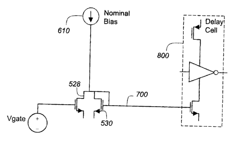
Refernng to Fig. 18, there is illustrated in a simplified schematic, an
implementation
of the bleeder device 528 for both positive and negative bias. By using a band
gap,
1. 30 the circuit of Fig. 18 provides PTAT current, that to a first order
helps to reduce
template dependence of the current. The Vgate nodes are provided by resistors;
which give a desirable instant voltage regardless of MOS processes.
CA 02455276 2004-O1-16
Similarly, a bleeder circuit using PMOS devices is used for P bias. This also
has an
added benefit of adjusting for odd process corners when P and N devices do not
track
one another (e.g., strong N, weak P and vice versa) since they are adjusted
separately.
1. 5
It may be understood by those skilled in the art that variations may be made
to these
implementations while still implementing the essential inventive concept.