Note: Descriptions are shown in the official language in which they were submitted.
CA 02455572 2008-05-08
30276-6
DIMMER CONTROL SWITCH UNIT
SPECIFICATION
Technical Field
This invention generally relates to a light dimmer control system, and more
particularly,
to a dimmer control system employing a master unit in communication with one
or more remote
units.
Background of Invention
Dimmer Iigliting and control systems are widely used in indoor lighting to
provide a
softer feel and more controllable illumination experience as compared to
on/off lighting. Prior
dimmer lighting systems have employed dimmer switch controls that include an
on/off switch
and an up/down power control, master unit and remote units, and microprocessor
control for
various power-up, power-down and fade in/out functions. Rather than use a
variable resistor
type rheostat which wastes power and generates heat at low illumination
levels, modem
dimming systems employ phase regulation, in which the power circuit is
switched on.at a time
delay following a zero-crossing of the AC sine wave input until the end of
each half cycle in
order to supply a variable level of power to the lighting load.
However, prior multi-location dimmer control systems have various shortcomings
and
problems in operation. In systems that employ master and remote units, the
remote units are
"dumb" boxes that simply have on/off and up/down switches but do not indicate
the lighting
status of the system. Attempts to provide two-way communication functions
between the master
and remote units would impose added costs and difficulties in outfitting the
remote units with
power sources and the capability to communicate with the master unit.
-1-
CA 02455572 2008-05-08
30276-6
For example, a typical prior art multi-location dimmer (shown in Figure 5)
consists of a
fully functional master unit and a number of remote units (1, ... n), where
the remote units are
connected in parallel with each other between a "switched hot" line of the
master unit and a
"Traveler" or "Control" line of the master unit. The remote units communicate
to the master
unit by sending a portion of the output current on the Traveler line to the
control input of the
master unit. To transmit three commands (Up, Down, and Toggle On/Off),
positive, negative
and alternating waveforms are used. These remote units require no power in
normal operation,
and cannot display the level of light setting. To display the light setting
level, the remote units
would require power and two-way communication means. The task of supplying
power to the
remote units is quite complicated, as every remote would need some current to
operate. With
the remote units connected in parallel, total current drawn from the control
terminal of the
master unit unit would be proportional to the number of remote units connected
to the system.
When this curreiit reaches a certain level, the lamp load may start glowing
(showing
illumination) wheii it is supposed to be in the Off condition. Also the power
supply size needed
would increase in proportion to the maximum number of remote units that could
be connected to
the system.
For a multi-location dimmer that supplies power to the remote units, there may
be a
problem that the internal dimmer's power supply could create an audible noise
in the load when
the load is Off, which otherwise would be masked when the load is On. This
power supply may
also generate waste heat.
It is also lrnown in prior dimmer control systems to use control memory to
restore the
illumination level to the same level as when it was last powered off, as a
user often sets the
illumination level to a desired comfort level and wants the same level when
turning the light
system back on again. However, the use of a separate latch device is limited
to memorizing only
whether the load was on or off, and the use of ongoing memory storage of the
current power
level requires use of a memory component capable of extremely high usage of
read/write cycles,
which imposes an added cost.
-2-
CA 02455572 2008-05-08
30276-6
Summary of Invention
In accordance with one aspect of the present
invention, there is provided a power control switch unit for
controlling an amount of power delivered to a load, the
switch unit having a bottom housing, comprising: (a) a cover
frame mounted over the bottom housing; (b) a push-button
type actuator switch plate mounted for movement in the cover
frame, wherein the actuator switch plate has one
longitudinal side mounted on a switch hinge axis to a
stationary portion of the cover frame, and an opposing side
therefrom that is hingedly movable against a spring force
for movement by user actuation thereof; (c) a light
indicator display for visually indicating a power level to
be delivered to the load, wherein said light indicator
display includes an array of openings or lenses formed in
the actuator switch plate for terminating a series of light
pipes optically connecting a plurality of LEDs on a control
circuit board positioned in the bottom housing, and said
array of operiings or lenses are positioned on the one
longitudinal side of the actuator switch plate and aligned
with the switch hinge axis, in order to minimize
displacement of the light pipe ends from the LEDs on the
control circuit board when the actuator switch plate is
actuated.
In accordance with another aspect of the present
invention, there is provided a dimmer control switch unit
comprising: (a) a cover frame mounted over a bottom housing,
the cover frame having a generally rectangular shape; (b) a
push-button type actuator switch plate mounted for ON/OFF
movement in the cover frame, wherein the actuator switch
plate has one longitudinal side mounted on a.switch hinge
axis to a stationary portion of the cover frame, and an
- 2a -
CA 02455572 2008-05-08
30276-6
opposing side therefrom that is hingedly movable against a
spring force for ON/OFF movement by user actuation thereof;
(c) an UP/DOWN switch also accessible through the cover
frame for act:uating dimmer control circuitry on a control
circuit board positioned in the wall outlet box in order to
set dimmer power levels up or down in accordance with user
input; and (d) a power-level light indicator display
provided in the switch unit for visually indicating the
dimmer power level set in accordance with user input,
wherein said power-level light indicator display includes an
array of openings or lenses formed in the actuator switch
plate for terminating a series of light pipes optically
connecting a plurality of LEDs on the control circuit board
which are selectively lit in order to provide a visual
representation of the dimmer power level set in the dimmer
control circuitry, and said array of openings or lenses are
positioned on. the one longitudinal side of the switch plate
and aligned with the switch hinge axis, in order to minimize
displacement of the light pipe ends from the LEDs on the
control circuit board when the switch plate is actuated for
ON/OFF movement.
In accordance with another aspect of the present
invention, a dimmer control system is provided with a
communication control loop that connects a master unit in
series with the source and the load,
- 2b -
CA 02455572 2004-01-21
CWD-026969
and a plurality of remote units in series with each other between the
"Switched Hot" line and the
"Traveler" or "Control" line of the master unit, and the communication control
loop is
superimposed on the dimmer load line in a manner that allows two-way
communication between
the master unit and the remote units without any effect from the dimmer load
current on the
communication. Communication messages from the master unit to the remote units
are encoded
in loop current fluctuations that are decoded by the remote units, and
communication messages
from any remote to the master unit are encoded in loop voltage fluctuations
that are decoded by
the master unit.
In a preferred embodiment of the invention, the communication control loop
connects the
master unit's control circuit in series with the respective remote units so as
to minimize the
current requirements and the required power supply size. The master unit uses
a switched power
supply during normal operation. The communication loop is hosted and
synchronized by the
master unit, and the communication messages are transmitted close to the
timing of the input
line voltage zero crossings, i.e., at the beginning of each half-cycle of
input line voltage. The
master unit's power circuit provides an output rail voltage equal to the sum
of the total control
loop voltage drop attributable to the series-connected control circuits of the
remote units and a
fixed reference voltage. The reference voltage for the power supply is tied to
the control loop
voltage drop, thus generating minimum heat regardless of the number of remote
units in the
loop.
As a further aspect of the present invention, the master unit's power circuit
maintains its
switched power supply in tandem with a capacitive power supply. The switched
power supply
is used during normal LOAD ON conditions, whereas the capacitive power supply
is used to
continue to supply power to the system during LOAD OFF conditions, when the
switched power
supply is switched off in order to avoid acoustic noise (hum) in the load. The
switched power
supply with floating reference voltage powers the system during normal LOAD ON
conditions
in order to avoid the heat generation that would be incurred by otherwise
using a capacitive
power supply.
As another aspect of the invention, the master unit's control circuit includes
a non-
volatile memory that is written with system status information when a POWER
OFF condition is
detected. When a POWER ON condition is restored, the stored system status
information is
used to restore the operation of the dimmer control system to where it was
before the POWER
OFF condition. In the preferred embodiment, a POWER OFF condition (power
interruption) is
-3-
CA 02455572 2004-01-21
CWD-026969
detected when two consecutive zero crossings are not detected by the
microprocessor, and the
system status information temporarily stored in its RAM is recorded in the non-
volatile memory,
using the energy accumulated in a reservoir capacitor to power the recording
process.
As yet another aspect of the invention, the master and remote units have a
physical
configuration in which an ON/OFF switch component is hinged for slight
actuator ON/OFF
movement on a hinge axis along one lateral side of the unit's frame, and a
system status display
is formed by an array of light indicators comprising a row of indicator lenses
arranged in the
surface of the ON/OFF switch component and aligned in close proximity in
parallel with the
hinge axis and optically connected by light pipes to respective LEDs on the
control unit's
control circuit board, wherein any slight displacement of the light pipes
caused by actuator
movement of the ON/OFF switch component can be minimized to avoid light
fluctuations in the
display of the indicator lenses.
Other objects, features, and advantages of the present invention will be
explained in the
following detailed description of the invention having reference to the
appended drawings.
Brief Description of Drawings
Figure 1 is a schematic diagram of a dimmer control system in accordance with
the
present invention, in which a communication loop connects a master unit in
series with a
number of remote units and is superimposed with a load line supplying power to
a load.
Figure 2 is a circuit diagram of the power circuit for the dimmer control
system of the
invention.
Figure 3 is a circuit diagram of the master unit's control circuit for the
dimmer control
system of the invention.
Figure 4 is a circuit diagram of the remote control circuit for the dimmer
control system
of the invention.
Figure 5 is a schematic diagram of a prior art dimmer control system showing a
master
unit connected in parallel with a number of remote units which do not have the
capability to
-4-
CA 02455572 2004-01-21
CWD-026969
communicate with the master unit or to show the lighting level.
Figure 6 shows timing diagrams illustrating the communication procedure of
master unit
communication and remote unit communication in relation to the timing of the
input line
voltage.
Figures 7A to 7D show a preferred structure for the master and remote units
having an
array of light pipe lenses displayed on a large ON/OFF actuator switch.
Detailed Description of Invention
A preferred embodiment of the invention is herein described in detail, and is
sometimes
referred to as the "Smart Dimmer" system. It is to be understood that while a
particular system
configuration, circuit layouts, and modes of operation are described, other
modifications and
variations may be made thereto in accordance with the general principles of
the invention
disclosed herein.
The Smart Dimmer is a wall-mounted, electronic system for controlling the
level of
power delivered to a load, such as a light, lamp or fan, thereby also
controlling the load's output
(e.g., light intensity). The Smart Dimmer system may be installed with one
"master unit" alone
or in combination with one or more "remote units" each having a bottom housing
for holding all
of the electronic components and a cover including a frame portion on actuator
switches for
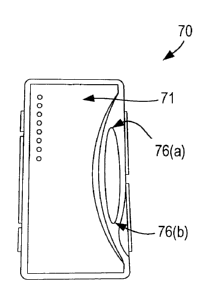
actuating the ON/OFF or dimming functions. Referring to Figure 7A, a preferred
design for the
cover 70 of the master and remote units is shown. The cover 70 includes a
frame portion 72,
shown separately in Figure 7C, to which a large actuator switch plate 71 is
mounted for push-
button type ON/OFF movement against a spring force (not shown). The back side
of the large
actuator switch plate 71 is shown in Figure 7B, and the back side of the frame
portion 72 with
the switch plate 71 mounted therein is shown in Figure 7D. A rocker-type
dimmer switch 76
projects through an oval aperture in the frame portion 72 and has ends 76(a)
and 76(b) which are
coupled to UP and DOWN switches on the control board in the bottom housing
(not shown).
The switch unit's frame portion 72 has a pair of spaced-apart switch hinge
pins 73a and
73b formed on opposing ends of the frame portion 72 to form a switch hinge
axis SH in
proximity to one longitudinal side of the frame portion 72. Each of the switch
hinge pins 73a
-5-
CA 02455572 2004-01-21
CWD-026969
and 73b, respectively, snap fits into recesses 74a and 74b formed on the back
side of opposing
ends of the large actuator switch plate 71 to form a switch hinge axis SH in
proximity to one
longitudinal side of the large actuator switch plate 71, allowing the opposing
side of the switch
plate 71 (formed with a concave shape) to be depressed against a spring force
for toggling
ON/OFF. An array of openings (or lenses) 75 also aligned with the switch hinge
axis SH are
formed in the large actuator switch plate 71 for terminating a series of light
pipes 75a optically
connecting the lighting level indicator LEDs on the control circuit board for
the unit located in
the bottom housing behind the cover 70. The alignment of the LED light pipe
array 75 with the
switch hinge axis SH ensures that there is only minimal displacement of the
light pipe ends from
the LED light sources when the large actuator switch plate 71 is depressed,
thereby minimizing
any illumination fluctuations in the external light indicator array. Once the
light pipes 75a are
attached to the large actuator switch plate 71, they become integral with it.
This arrangement of
fixing the light pipes 75a to the large actuator switch plate 71 along its
switch hinge axis SH
avoids problems related to having to provide clearance holes for the light
pipes in the large
actuator switch plate if the light pipes were otherwise fixed to the frame
portion or other non-
moving component. Placing the lighting level illumination display on the
switch plate 71 allows
the user to find and be guided to the operative part of the switch plate in
low light conditions and
provides an aesthetic feature to the overall system design.
The microprocessor-based control circuit controls the level of power delivered
to the
load in response to input signals generated by a user's actuation of the
ON/OFF and UP/DOWN
dimmer switches. For example, the device can be used to fade the load ON and
OFF, to increase
(brighten) or decrease (dim) power delivered to the load, and to perform
certain other fade
functions, all depending on a user's input. The Smart Dimmer's ON/OFF switch
is actuated by
one short-duration push of the button (i.e., one tap) or by holding the button
down for at least
two (2) seconds. The UP/DOWN dimmer switch is actuated by pushing the
respective ends of
the rocker switch. Each of these actuations results in a different fade
function depending on the
state of the power level delivered to the load when the actuation occurs.
Further, actuation of
the UP/DOWN dimmer switch when the load is Off results in a setting of the
desired power
level to be supplied to the load when the ON/OFF switch is actuated. That is,
when the load is
Off, the UP/DOWN dimmer switch cannot be used to turn the load On.
The vertical series of apertures or lenses for the light emitting diodes
(LED), preferably
eight (8) in number, are provided on the Smart Dimmer's switch plate to
indicate the desired
load power or intensity level to the user at all times. For example, the
bottom LED is yellow
-6-
CA 02455572 2004-01-21
CWD-026969
and the remaining LEDs are green. Only two (2) of the LEDs (the yellow and one
green) are
illuminated at any one time, such that the yellow LED is a frame of reference
and the green LED
shows the present power level in relation to the yellow LED. In one preferred
embodiment,
when a user instructs the Smart Dimmer to apply power to the load, the
activated LEDs are both
fully illuminated and when a user instructs the Smart Dimmer to remove power
from the load ,
the activated LEDs are both dimmed. Alternatively, the LEDs may remain at a
constant
brightness, or the LEDs can be caused to change color to indicate when the
power delivered to
the load should be ON or OFF.
The LEDs of the Smart Dimmer system are not operated directly by the power
supply.
The Smart Dimmer system also does not incorporate any direct means to sense
the load status.
The LED brightness or color change is a function of the software operation in
response to user
actuation, not affected by either the power supply or the actual load status.
It is supposed to
indicate the desired load status to the user, but has no direct means to tell
if the load is actually
energized.
Dimmer Control System
As shown in Figure 1, the dimmer control system is provided with a
communication
control loop that connects the master unit 10 in series with a plurality of
remote units (1, ... n)
labeled with reference numeral 20. The master unit has an LED Display for
indicating the
lighting status of the system, and a Power Board connected to a Control Board
for phase
controlling of an"AC Switch" positioned between the "hot" side of the dimmer
load line and the
"switched hot" side, which is connected to the Load. The master unit's Control
Board also
controls a Current Source to the series loop through the remote units. Each
remote unit 20 also
has an LED Display to indicate the lighting status of the system, and a
Control Circuit Board for
handling user inputs to the remote and the two-way communication functions
with the Master
Unit. The return line from the remote units is connected to the output
terminal of the master unit
("Switched Hot" terminal). The series loop enables two-way communication
between the
master unit and the remote units without affecting the operation of the dimmer
load line. As
described in further detail below, communication messages from the master unit
to the remote
units are encoded in loop current fluctuations that are decoded by the remote
units, and
communication messages from any remote to the master unit are encoded in loop
voltage
fluctuations, which are decoded by the master unit. The use of separate
encoding schemes
allows the one series loop to be used for the communication function without
confusion between
the Master and remote units and without needing complex communications
procedures.
-7-
CA 02455572 2004-01-21
CWD-026969
Circuit Operation: Control Board and Power Board
The Power Supply of the Master Unit generates DC rail voltage from the input
AC
sufficient to power the master unit's Control Board, Current Source and a
number of remote
units connected in series between the output of the Current Source and the
Switched Hot output
of the master unit. The Current Source generates DC current that flows through
the master
unit's Control Board and the remote units in the loop. This current generates
voltage for the
corresponding circuit operation in every remote and the master unit's Control
Board. The total
voltage drop across all the remote units in the loop is sensed by the Power
Supply, and the rail
voltage is self-adjusted accordingly. The use of n remote units in serial
connection simplifies
the Power Supply design and reduces the amount of heat generated by the
circuit. The "current
source" arrangement makes the communication loop virtually insensitive to
ripple and noise.
Referring to Figure 2, the Power Board circuit of the master unit is connected
in series
with the load, with a LINE IN terminal attached to a power line and a DIMMED
LINE terminal
connected to the load. The system does not require a neutral connection. The
Power Supply
consists of a switched power supply formed around darlington pair Q3 and Q4
for normal
LOAD ON operation, in tandem with a capacitive power supply formed around
capacitor C 1 for
LOAD OFF conditions. The Power Board circuit also provides a Current Source
for the LOOP
CONTROL to the remote units formed around transistor Q6. The remote units are
connected in
series with each other, with the first remote unit connected between the LOOP
CONTROL
terminal of the Master Unit and the next remote unit, and the last remote unit
connected between
the previous remote unit and the DIMMED LINE terminal of the master unit.
Thus, all remote
units are connected in a loop between the DIMMED LINE and LOOP CONTROL
terminals of
the master unit. The Power Board circuit of the master unit is interconnected
to the Control
Board circuit by interconnection through a 6-pin header J1.
Referring to Figure 3, the Control Board circuit of the master unit is
interconnected via
header J1 with the Power Board's circuit. The Control Board circuit comprises
a micro-
controller U1, three push-buttons (UP, ON/OFF, and DOWN), and a switchable
current source
built around transistor Q1 to control the gate of the triac switch Q1 on the
Power Board. When
the switchable current source receives a control signal from the micro-
controller Ul, it generates
gate current for the triac switch Q1 on the Power Board. The triac switch is
then conducting and
allows power to be conducted from the source to the load until the end of the
half-cycle. When
the control circuit is not producing a control signal, the triac is not
conducting. Of the three
-8-
CA 02455572 2004-01-21
CWD-026969
push-buttons, the UP and DOWN buttons are formed by opposite ends of a rocker
switch on the
actual unit, and are used to gradually increase and decrease the power
delivered to the load,
respectively, and to change the preset level when the load is OFF, when the
buttons are pressed.
The ON/OFF button is used to commence a preprogrammed fade from ON to OFF or
from OFF
to ON depending on the current state and the user input. All fades are caused
by the micro-
controller sending control signals to either increase or decrease the amount
of time the triac
switch is conducting per cycle of the input AC waveform, thus controlling the
percentage (from
0-95%) of the AC waveform that is conducted from the source to the load.
Therefore, the Smart
Dimmer uses phase control to deliver power to the load in pulses, such that
the duration of the
pulses determines the power level.
Referring to Figure 4, each of the remote units contains a similar Control
Board with
micro-controller U1 as used in the master unit, but do not contain the Power
Board. The Control
Board in the remote units is used mainly to receive commands from the master
unit, and to
display the lighting level status accordingly. The remote unit's Control Board
is also used to
generate the UP, DOWN and ON/OFF switch commands, which are encoded in loop
voltage
fluctuations and decoded as a digital sequence by the master unit, when the
corresponding
switches are actuated. The remote units do not store any information regarding
the triac switch's
firing angle or ON/OFF status.
Floating Reference Voltage for Control Circuits & Communication LooP
The loop current generated by the current source Q6 (Figure 2) produces some
voltage
drop across the control loop. This voltage drop is proportional to a number of
remote units in
the loop. It also includes the voltage drop produced by wiring itself. The
resulting voltage drop
including the voltage drop across a protection diode D11 applies to the
collector of Q6. After
passing through a low pass filter R17, C8, the voltage applies to the base of
Q9 (Fig.2) that is
configured in an emitter-follower arrangement and provides a voltage-following
effect. The
emitter voltage of Q9 follows the base voltage, while keeping the emitter at
about 0.6V higher
level than the base. The low impedance of the emitter Q9 makes it a reference
point for the
power supply. The regulation process of the power supply is described below.
When the Load is on, with every positive half cycle of the power line when the
momentary voltage gets higher than the rail voltage, the Darlington transistor
Q3Q4 starts
-9-
CA 02455572 2004-01-21
CWD-026969
conducting. The capacitor C6 gets charged through the load resistance and D2,
R6 and Q4.
When the voltage on C6 goes above the sum of the reference voltage at the base
of Q9 and the
Zener diode D7 voltage, the diode D7 breaks over, and passes the current
through the gate of the
SCR X2. The SCR starts conducting, and shunts the Darlington Q3Q4 base
current. The
Darlington Q3Q4 stops conducting, and the capacitor C6 starts discharging
through the current
source Q6. The cycle repeats every positive half cycle of the power line. Even
if the condition
of the control loop changes, the rail voltage (voltage on C6) is always kept
at about 13v above
the control loop voltage drop. The rail voltage in this circuit can range from
+13v to +55v
depending upon the number of remote units and conditions in the communication
control loop.
The communication pulses and noise do not affect the rail voltage due to the
low-pass filter R17,
C8. The maximum rail voltage is limited by a Zener diode D13.
When the Load is off, the capacitive power supply output voltage is regulated
by the
Zener D7, and the gate-to-cathode voltage of the SCR X2. The resulting rail
voltage is about 2V
higher due to the voltage drop across R11, which is needed to automatically
turn the switching
supply off. The maximum rail voltage in this case is limited by Zener D14.
Circuit Operation of Master/Remote Communication
Communication in the Smart Dimmer system is achieved by transmitting encoded
current fluctuations from the master unit to all the remote units, and
transmitting a message
encoded in voltage fluctuations from a remote to the master unit whenever the
remote is
actuated. The procedures for sending the communication messages are described
below.
For communications from the master unit, the master unit Control Board
manipulates the
Current Source to modulate the loop current. The loop current passes through
every remote and
is detected as a dropout voltage across the resistor R in every remote. The
loop current
modulation thus results in the resistor R dropout voltage change, which is
picked up and
decoded as a digital message by the microprocessor in each remote's Control
Circuit. The
digital message from the master unit contains information that enables the
remote's
microprocessor to retrieve the display information to implement the
corresponding LED display
brightness and series lighting pattern, thus synchronizing the LED displays in
the master unit
and the remote units.
-10-
CA 02455572 2004-01-21
CWD-026969
Referring to the master unit Power Board circuit in Figure 2, the current
source Q6
supplies current for the system operation. The same current powers all the
remote units in the
loop, as well as the Control Board of the master unit. Thus, the total current
drawn from the
Power Supply is minimized and independent of the number of remote units in the
loop. An
added benefit of this solution is a very good power supply ripple rejection.
When no
communication is required, the communication loop is powered by a constant DC
current. The
base of Q6 is fixed at -7.5V off the power rail. The emitter of Q6 is
connected through the
resistors R12, R18 in Figure 3 and a controlled Zener diode U2 to the same
power rail through
interconnect Pin 1 of the header J1. This results in the Q6 emitter current of
about 12mA. This
DC current powers the Control Board circuitry, and the operation voltage of
3.5V is stabilized
by the controlled Zener diode U2. Assuming Q6 is a high gain Darlington
transistor, its
collector current is very close to 12mA also. This current flows through the
control loop and
powers all the remote units. It passes through a diode bridge D1 in the
remote's Control Board,
which makes the remote units unidirectional, and it drops 3.5V required for
the remote circuitry
operation on a controlled Zener diode U2 (Figure 4). After that it passes
through a resistor R12
and back to the loop through the diode bridge D 1.
The DC current level is considered a low logic level (logic "0") in the
downstream
communication from the master unit to the remote units in the loop. To
transmit a high (logic
"1") logic level, output pin 12 of the MPU U 1(Figure 3) on the master unit
Control Board goes
low, and turns a switch Q3 on. This results in a loop current increase by
about 5mA. The loop
current increase results in the R12 voltage drop increase of about 1 V in
every remote in the loop
(Figure 4). This voltage drop change goes through the DC blocking capacitor C8
into input Pin
11 of the MPU Ul. This input is configured as an analog comparator input.
Resistors R14, R20
provide a DC bias about 0.5V above the internal reference voltage of the
analog comparator.
Thus the comparator converts the transitions of the voltage drop across R12
into a digital
sequence further processed by the CPU.
When a Remote button is actuated, the Control Circuit of the remote
manipulates the
switch SW to modulate the voltage drop across the remote. This modulation is
picked up and
decoded by the master unit. The message from the remote contains information
about which
button has been actuated on the remote. With the DC loop current, the Control
Loop exhibits a
certain voltage drop that is a sum of the voltages drop across every remote in
the loop and the
wiring voltage drop. The loop voltage drop under no communication conditions
is considered a
low logic level (logic "0") in the upstream communication from the remote
units in the loop to
- 11 -
CA 02455572 2004-01-21
CWD-026969
the master unit. To transmit a high (logic "1 ") logic level, output pin 12 of
the MPU U 1(Figure
4) in the remote goes low, and turns a switch Q3 on. This results in a
decrease of the voltage
drop across this remote and the whole loop by about 1 V. This transition is
applied to the
collector of Q6 (Figure 2), and goes as a negative polarity pulse through the
DC blocking
capacitor C4. This pulse applies to the emitter of Q7 through the resistor
R20, and generates a
current pulse at the collector of Q7. This current pulse flows from the power
rail through R20
(Figure 3) into the collector of Q7 (Figure 2), and generates a voltage drop
on the resistor R20
(Figure 3), which is sensed by input Pinl1 of the MPU U1. This input is
configured as an
analog comparator input. The comparator converts the transitions of the
voltage drop across
R20 into a digital sequence further processed by the MPU as remote button
activation
information.
The communication from the master unit is timed to occur close to the power
line
voltage zero crossings to minimize the effect of noise on data integrity.
While the master unit is
directly synchronized from the power line, the remote units use the master
unit's message to
synchronize their transmission. The diagram in Figure 6 illustrates the
communication
procedure. At the beginning of every positive half cycle of the power input,
the master unit
transmits a communication decoded as a digital message to the remote units in
the Control Loop.
The transmission occurs quite close to the voltage zero crossing to minimize
power line noise
effect on the communication. The message contains information about the
pattern and
brightness of the master unit's LED display. Remote units receive the message
and adjust their
LED displays accordingly. Every message from the master unit begins with a
start bit. Remote
units recognize this bit as the beginning of the frame, and use it to start a
software timer that
places a response message, if any, close to the next voltage zero crossing (at
the half cycle). The
response message is generated only if any of the buttons on the remote is
actuated. If the
message does not match the frame size or is not recognized by a remote, it is
rejected. As the
response messages from the remote units are synchronized with the master
unit's transmission,
the master unit uses gating to minimize noise effect on the received signal
integrity. The
received message is accepted only within a predetermined time frame. If the
message does not
match the frame size or is not recognized by the master unit, it is rejected.
The gating technique
is essential for the upstream communication, because it is received at a high
impedance node
represented by the output of the current source. The downstream communication
is much less
sensitive to the noise, as the remote's impedance is quite low.
-12-
CA 02455572 2004-01-21
CWD-026969
When two or more remote units get actuated at the same time, they produce
synchronous
messages for the master unit. If the same button of the remote units is
actuated the amplitude of
the communication signal is increased. That will cause a larger current pulse
through the
resistor R20 (Figure 3). In this case the amplitude of the pulse at Pin 11 of
the MPU U1 will be
limited by the MPU's internal input protection diodes, and the message will be
accepted by the
master unit. The message structure is designed such that, if different buttons
of two or more
remote units are actuated, the resulting combination message will not be
recognized by the
master unit, and will be rejected.
The power level indicated by the LEDs of the control units are not operated
directly by
the power supply. The power supply (either capacitive or switching) maintains
a voltage level
on the power rail with respect to the common conductor. This voltage is
converted to constant
current by the current source based on Q6 (Figure 2) as explained earlier.
Almost the same
current flows in the emitter and collector circuits of the Q6. The collector
current is being used
to power the remote units control circuit board (if any of them are used). The
emitter current is
used to power the master unit's control circuit board.
As the remote and master unit control circuit boards operate the same way, the
following
description explains the LED operation with reference to Figure 3. The current
generated by the
current source flows from J1 Pinl (connected to the power rail on the master
unit power board)
through a controlled zener U2 and resistors R12, R18 to Jl Pin3, which is
connected to the
emitter of Q5 on the master unit power board. The 3.5V developed across U2 is
used to power
the control board circuitry. There are 7 green and one yellow LED on the
control board. The
yellow LED is always on. It is powered through a voltage regulator Q2, and a
current limiting
resistor R9. The green LEDs are powered through the voltage regulator Q2 and a
current
limiting resistor R5. The green LEDs are switched on and off by the MPU UI.
Only one of the
7 green LEDs is on at a time. Brightness of the LEDs is defined by the status
of Pin20 of the
CPU UI. When the level on Pin20 is high the LEDs are bright, when the level is
low, the LEDs
are dim. The status of the LEDs (which one is lit, and its brightness) is
defined by a 8-bit digital
word loaded into Portl of the MPU U1 configured as an output. The word is
calculated by a
subroutine based on the projected firing angle of the main triac and the value
of the Light On
flag in the Status register for the master unit unit. The same word is derived
from the
communication signal for the remote(s). The Light On flag indicates that the
triac control signal
generation is allowed. It does not coincide, though, with the triac control
signal per se. In the
same way, the Pin20 status change does not coincide in time with the Light On
flag change.
-13-
CA 02455572 2004-01-21
CWD-026969
Pin20 of the MPU has no electrical connection with the triac control circuitry
and cannot be
used to assess the status of the load. Pin2O controls the base of the
transistor Q5 on the control
board, which in turn generates the control signal for the gate of X1 on the
power board to switch
the capacitive power supply on and off as discussed above.
Switched/Capacitive Power Supply
Due to the fact that the Smart Dimmer System components are connected in
series the
Power Supply has to produce the rail voltage sufficiently high to accommodate
the voltage drop
across all the components. In the meantime, the output current required to
power the control
circuit is low and does not change with the number of remote units used in the
system. The
trade-off "higher voltage vs. lower current" is favorable, as the circuit does
not generate much
heat while dropping the line voltage to the desired level.
The Smart Dimmer system features two power supplies located on the Power Board
of
the master unit. These power supplies are a switching one and a capacitive
one. The power
from the source is derived through the load. In the Power Board circuit
diagram in Figure 2, the
switching power supply consists of a solid-state switch - Darlington Q3 and Q4
and associated
circuitry. It operates only during a short period of time at the beginning of
a positive half cycle
of the power line voltage. This voltage is applied through D2 and R5 to the
anode of D5. When
the momentary voltage builds up, and gets above the DC level on the positive
lead of the
reservoir capacitor C6 (referred to herein as "the power rail"), the diode D5
starts conducting
and Darlington Q3-Q4 goes into saturation. The power line current limited by
the load
impedance and a resistor R6 starts charging the capacitor C6. When the voltage
on C6 exceeds
the sum of a reference voltage on the emitter of Q9 and the breakover voltage
of the zener diode
D7, the diode D7 breaks over and passes current through to the gate of an SCR
X2. As the SCR
X2 starts conducting, the voltage on the anode of D5 drops below the rail
voltage, D5 stops
conducting, and the Darlington Q3-Q4 turns off. From this moment and to the
beginning of the
next positive half cycle, the capacitor C6 is being linearly discharged by a
current source built
around a PNP transistor Q6. Then the whole cycle repeats.
The base of Q9 is connected to the output of the current source built around
Q6 in such
way that it senses the total voltage drop of all remote units and wiring in
the communication
loop. Transistor Q9 is connected in an emitter follower configuration. The
voltage on the
-14-
CA 02455572 2004-01-21
CWD-026969
emitter of Q9 follows the sensed voltage drop in the communication loop. As
this circuit node
exhibits very low impedance, it represents a floating voltage reference point
for the power
supply. Thus, the rail voltage is always set about 13V higher than the
communication loop
voltage drop.
The capacitive power supply includes a voltage drop capacitor Cl, current
limiting
resistor R1, discharge diode D3, an SCR Xl, and a corresponding circuitry.
When a control
signal is received from the Control Board (LOAD OFF condition), the capacitive
power supply
starts working as follows. The positive half cycle of the power line voltage
passes through R1
and Cl. When the momentary line voltage exceeds the power rail voltage, with
D3 reverse
biased, the current flows through D4 and R8 to the gate of Xl. X1 starts
conducting and charges
C6 to a level somewhat higher than would be developed by the switching power
supply. This
level is defined by the value of CI and a total circuit current consumption,
which is constant in
this design. As the capacitor C6 charges up, the zener diode D7 breaks over,
and X2 turns on.
This prevents Q3-Q4 from turning on when the capacitive power supply is
operational. When
the momentary voltage of the positive half cycle goes down below the rail
voltage, X1 turns off,
Cl gets discharged by the negative half cycle, which goes through R1, Cl, and
the forward
biased D3. The operation repeats for every power line cycle.
When the control signal on Pin6 of J1 goes about -3v below the power rail
voltage, Xl
does not turn on, and the switching power supply resumes operation. This
control signal is used
to switch the capacitive power supply on when the load is not energized, and
the "silent"
operation of the circuit is desired. When the load is on, the current limiting
resistor RI of the
capacitive power supply would generate significant amount of heat. That is why
the capacitive
power supply is used when the load is off, and the switching one is used when
the load is on.
In the master unit Control Board circuit diagram depicted in Figure 3, when
Pin 20 of
the microcontroller Ul is at logical "0" (low level), the transistor Q5 is not
conducting. The
collector of Q5 exhibits high impedance. The SCR X1 on the power board turns
on at every
positive half cycle, as explained above, and the capacitive power supply is
operational. The
Smart Dimmer system thus operates in a "silent mode". When Pin 20 of the
microcontroller U 1
goes to logical "1" (high level), the transistor Q5 starts conducting and
connects the gate of the
SCR X1 (Pin6 of J1) to the common point of the Control Board, which is about
3V below the
power rail voltage. This stops the capacitive power supply, and resumes the
switching power
supply operation.
-15-
CA 02455572 2004-01-21
CWD-026969
Power Interruption Memory
The master unit also includes a power interruption detection circuit and
system memory
for saving and then restoring the system's power level to the load after a
power interruption to
the level in effect immediately prior to the power interruption. During
regular operation, the
micro-controller identifies the power level as a 16-bit binary number and
regularly stores that
number in the micro-controller's RAM. The binary number represents the time
delay for
switching on the main triac Q 1 on the Power Board which determines a
percentage of the input
AC power delivered to the load. When the source power is interrupted (i.e.,
when no further
zero crossing of the AC input power is detected as a power cut-off by the
micro-controller), the
reservoir capacitor of the Power Supply supplies enough power to enable the
micro-controller to
store the latest binary number from RAM into its flash (non-volatile) memory.
Thereafter, no
power needs to be supplied to the micro-controller until the main power source
is restored. The
micro-controller's flash memory is static, non-volatile and requires no power
(and therefore no
auxiliary power source) to maintain the stored binary number in flash memory.
When source
power is restored to the micro-controller, the binary number is recalled from
flash memory to
RAM, calculations are performed to determine the last power level, and the
micro-controller
gates the triac Q 1(Figure 2) at the appropriate delay times from zero
crossings along the source
AC waveform to restore the power level to the level prior to the power
interruption.
In this manner, the system status information prior to power interruption is
stored in the
microcontroller's internal non-volatile memory (or an external memory chip)
only when a power
interruption has been detected. This avoids constant writing of the status
information into non-
volatile memory, which can cause the memory to fail after repeated writings
exceed its service
life. By using the energy accumulated in the reservoir capacitor to power the
recording process,
the need for an auxiliary power supply is avoided.
It is understood that many modifications and variations may be devised given
the above
description of the principles of the invention. It is intended that all such
modifications and
variations be considered as within the spirit and scope of this invention, as
defined in the
following claims.
-16-