Note: Descriptions are shown in the official language in which they were submitted.
CA 02455855 2004-O1-29
WO 03/012936 PCT/GB02/03463
1
TUNEABLELASER
This invention relates to tuneable lasers and has particular, but not
necessarily exclusive, reference to tuneable lasers for use in
telecommunications systems operating in the C-band, namely within the
band of 1530 to 1570 nm. The embodiments concern in particular, but not
exclusively, four section distributed Bragg reflector tuneable lasers.
Background to the Invention
In this specification the term "light" will be used in the sense that it is
used
in optical systems to mean not just visible light but also electromagnetic
radiation having a wavelength between 1000 nanometres (nm) and 3000
nm.
Single wavelength lasers are important for a number of applications in
optical telecommunications and signal processing applications. These
include multiple channel optical telecommunications networks using
wavelength division multiplexing (WDM). Such networks can provide
advanced features, such as wavelength routing, wavelength conversion,
adding and dropping of channels and wavelength manipulation in much
the same way as in time slot manipulation in time division multiplexed
systems. Many of these systems operate in the C-band in the range 1530
to 1570 nm.
Tuneable lasers for use in such optical communications systems,
particularly in connection with the WDM telecommunication systems, are
known. A known tuneable system comprises stacks of single wavelength
distributed Bragg reflectors (DBR) lasers, which can be individually
selected, or tuned over a narrow range, or by a wide tuning range
tuneable laser that can be electronically driven to provide the wavelength
CA 02455855 2004-O1-29
WO 03/012936 PCT/GB02/03463
2
required. Limited tuning range tuneable lasers that rely upon thermal
effects for tuning are also known.
US-A-4896325 discloses a wavelength tuneable laser having sampled
gratings at the front and rear of its gain region. The laser described in that
specification relies on the use of two different gratings which produce
slightly different reflection combs in the front and rear gratings. These
provide feedback into the device. The gratings can be current tuned in
wavelength with respect to each other. Co-incidence of a maximum from
each of the front and rear gratings is referred to as a supermode. To
switch the device between supermodes requires a small incremental
electrical current into one of the gratings to cause a different pair of
maxima to coincide in the manner of a vernier. By applying electrical
currents to the two gratings so that the corresponding maxima track,
continuous tuning within a supermode can be achieved.
In summary, for a given set of drive currents in the front and rear grating
sections, there can only be a simultaneous correspondence in reflection
peak at one wavelength, as a consequence of which the device lases at
that wavelength. To change that wavelength a different current is applied
to the front and rear gratings. Thus the front and rear gratings operate in a
vernier mode, in which the wavelengths of correspondence determine a
supermode wavelength.
An improved form of selective grating is the phase shifted grating, as
described in UK-A-2 337 135, the contents of which are incorporated
herein by way of reference.
The term "phase shifted grating" as used herein is used to describe and
define a selectively reflecting distributed Bragg grating which is
constructed and operates in the manner described and claimed in UK-A-2
337 135. In other words, a phase shifted grating is one in which the grating
CA 02455855 2004-O1-29
WO 03/012936 PCT/GB02/03463
3
structure comprises a plurality of repeat gratings in which each grating unit
comprises a series of adjacent diffraction gratings having the same pitch,
and is characterised in that the grating units and adjacent gratings within a
grating unit are separated by a phase shift of substantially pi (~) radians
and in which at least two of the gratings within a grating unit have different
lengths, the lengths being selected so as to provide a predetermined
reflection spectrum.
Details on the construction and operation of the phase shifted- grating are
to be found in UIC-A-2 337 135. The Bragg gratings may be defined using
e-beam writing onto suitable photoresist as a processing step.
Summary of the Invention
By the present invention there is provided a tuneable laser having a gain
section bounded at one end by a first reflector in the form of a distributed
Bragg reflector adapted to produce a comb of reflective peaks and on the
other end by a second Bragg reflector, the second Bragg reflector adapted
to reflect at a plurality of wavelengths and being capable of being varied
selectively through discrete segments so that one or more segments of the
Bragg reflector can be tuned to a lower wavelength to reflect with a
segment reflecting at that lower wavelength to enhance the reflectivity at
that lower wavelength.
The lower wavelength to which the second reflector is tuned may
substantially coincide with a peak of the first reflector.
The second reflector may be formed in a material having a variable
refractive index and the variation of the reflected wavelength may be
affected by varying the refractive index of the material.
CA 02455855 2004-O1-29
WO 03/012936 PCT/GB02/03463
4
The refractive index may be varied by passing an electrical current via
electrodes through the material in which the second reflector is formed.
The second Bragg reflector may be a chirped grating and may be formed
in a material having a refractive index variable in response to the passage
of current therethrough, there may be a plurality of external electrodes
along the length of the grating, with each electrode being selectively
connectable to a power source.
The second Bragg reflector may comprise a plurality of discrete grating
segments, at least two of which grating segments may have a different
pitch wherein current may be applicable to at least the grating having a
longer pitch such that the effective wavelength of the grating having a
longer pitch can be tuned to the wavelength of the grating having a shorter
pitch.
The chirped Bragg reflector may comprise a linear chirp of progressive
pitch variation along the chirp with the shortest pitch closest to the gain
section.
The second Bragg reflector may comprise a plurality of discrete grating
segments, each grating segment having a different pitch, such that the
grating segment closest to the gain section has the shortest pitch, the pitch
of each successive grating segment from the gain section may be greater
than the pitch of the preceding segment.
Each grating segment may have an independently actuable electrode.
A switching circuit may be provided to switch the current to the electrodes.
The tuneable laser may be manufactured using semiconductor materials,
particularly using a III-V semiconductor material. It may be manufactured
CA 02455855 2004-O1-29
WO 03/012936 PCT/GB02/03463
using electron beam writing techniques or may be manufactured using a
holographic phase grating plate.
The Bragg segments in the second reflector may be each kept short so
that the cumulative waveguide length associated with the Bragg gratings is
minimised, thereby keeping the waveguide attenuation losses low.
The distributed Bragg reflector forming the first reflector may be a phase
shifted Bragg grating reflector, and light may be emitted through the
second reflector.
There may be a phase change section between the gain section and
either one or both of the reflectors.
The phase change section may be located between the gain section and
the first reflector.
Alternative arrangements of the segmented grating order are possible
within the scope of the invention.
Alternative arrangements of the chirp are possible for example, a non
linear progressive chirp, and the longest pitch being closest to the gain
section.
In the case where the second reflector is a chirped Bragg reflector it may
be considered as being partitioned into chirp segments each consisting of
part of the over all chirp grating, all chirp segments being concatenated.
Other means of varying the refractive index than a current could be used,
for example by thermal means, or use of an electric field.
CA 02455855 2004-O1-29
WO 03/012936 PCT/GB02/03463
6
By short Bragg segments is meant lengths such that the associated
reflectivity of each segment is broad and there is a degree of overlap
between neighbouring segment reflectivities. However, the segment
reflectivity discrimination is sufficient for stable lasing operation in
combination with reduced light power losses.
In one embodiment the first reflector comprising a distributed Bragg
reflector which is made long as herein defined.
"Long" as used in this context herein means as many repeat grating units,
as described in UK-A-2 337 135, as are required to produce sufficiently
narrow peaks for single longitudinal mode operation of the laser.
Preferably 10 or more repeat grating units are present.
The first reflector may also have an electrode to permit electrical current to
be passed through it to alter the wavelengths at which the comb of
reflecting peaks reflects.
The phase change sections) may have an electrodes) to permit the
passage of electrical current through the phase change sections) to alter
the refractive index of the material of the phase change sections) to affect
the phase change.
The refractive index of the material in which the front and rear Bragg
gratings are formed is variable simultaneously to affect fine tuning of the
laser.
The distances between the electrodes on the second reflector are short as
herein defined.
The grating of the first reflector may be long so as to produce reflection
peaks at well defined wavelengths.
CA 02455855 2004-O1-29
WO 03/012936 PCT/GB02/03463
a:~ a tt ~.~5 lr.~ ~.~e c~ d N~ a~ ~~~
7
Brief Descriation of the Drawings
Figure 1 is a schematic cross section through a laser in accordance with
the invention incorporating a segmented Bragg second reflector,
Figures 2a to 2e are graphs of intensity I vs. wavelength 7~, for the
segmented Bragg second reflector embodiment,
Figure 3 is a schematic cross section through a laser in accordance with
the invention incorporating a chirped Bragg second reflector,
Figure 4 shows a second embodiment of the invention,
Figure 5 shows a chirp grating,
Figure 6 shows a chirp line,
Figure 7 shows an enlarged view of light passing down a chirp grating,
Figures 8 and 9 show box diagrams of light intensity vs wavelength,
Figure 10 is an explanatory view of a chirp laser chirp line and light
intensity,
Figures 11 and 12 shows chirp line drawings, and
Figures 13a to 13e are graphs of intensity I vs. wavelength ~,, for the chirp
Bragg second reflector embodiment.
Description of the Preferred Embodiments of the Invention
The wavelengths of interest referred to above, for example the C-band
wavelengths of 1530 to 1570 nm are the wavelengths of light in free
space. When such light passes through a medium, of refractive index neff
the actual wavelength of the light within that medium, which will be
referred to herein as A', is the wavelength A divided by the value for the
refractive index Nee. In other words
~' _ ~le~.
where Neff is the effective refractive index of the medium as seen by the
propagating light of wavelength ~, in free space.
CA 02455855 2004-O1-29
WO 03/012936 PCT/GB02/03463
8
It so happens that the glass (silica) fibres, which are commonly used in
telecommunications systems, have low loss regions at about 1100 nm,
1300 nm and 1500 nm. These regions are about 100 nm wide and
consequently much work is done on producing lasers that produce light in
the low loss bandwidths. The same is true for the tuneable laser of the
present invention. The specific examples of the invention are designed to
work in the c- Band, but the invention could be used for other wavelengths
if required and if new types of fibre optical cables become available.
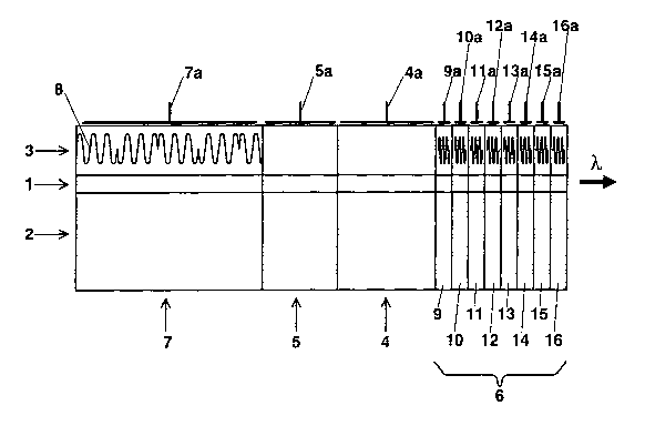
Referring to Figures 1 and 3, they show schematic cross sectional views of
a lasers in accordance with the present invention. As is conventional in
semiconducting lasers the laser is built up in a series of layers, with a
layer
1 formed between a lower layer 2 and an upper layer 3. Layer 1 bounded
by layers 2 and 3 forms a waveguide. There may be a plurality of layers in
the structure, but they are not material to the invention and for the better
understanding of the invention they are not shown.
In Figure 1 the laser itself has four principal sections. A gain section 4, a
phase change section 5 and front and rear reflecting sections 6 and 7. The
rear reflecting section 7 has a phase shifted grating distributed Bragg
reflector 8 formed in the layer 3. Such a reflector produces comb of
reflectance peaks at separated wavelengths, and each peak is of
substantially the same height. The front reflector 6 is made up of a series
of segments, each segment being a distributed Bragg reflector, each
segment centred at substantially a single wavelength with a broad
wavelength reflecting spectrum. The centre wavelengths of the individual
peaks of the segments 9 to 16 correspond to the peaks of the comb of
reflectance produced by the front reflector distributed Bragg reflector.
In Figure 3 the laser itself has four principal sections. A gain section 61, a
phase change section 60 and front and rear reflecting sections 62 and 50
respectively. The rear reflecting section 50 has a phase shifted grating
CA 02455855 2004-O1-29
WO 03/012936 PCT/GB02/03463
9
distributed Bragg reflector 51 formed in the layer 3. Such a reflector
produces a comb of reflectance peaks at separated wavelengths, and
each peak is of substantially the same height. The front reflector section
62 consists of a linear chirped grating of progressive pitch variation along
the length. Above the chirped grating are a series of individual adjacent
electrodes 65 through 72, that define sub-region chirped gratings that
together comprise the over-all chirped grating. Each of the sub-region
chirped gratings reflects over a range of wavelengths. In its passive state
the total reflection spectrum covers the band of interest with substantially
uniform reflectivity.
The invention design may be suitably applied to solid-state lasers
manufactured using Group III-V or other semiconductor materials.
In the case of the segmented Bragg grating front reflector four section
laser, the method of operation of the laser is more readily understood by
reference to Figures 2a to 2e. These drawings show aligned one above
the other the combs of reflectance produced by the front and rear
reflectors. In the drawings the intensity of reflectance I is plotted
vertically
against wavelength ~,. Fig 2a shows the comb of reflectances 29a to 36a
produced by the segmented gratings 9 to 16 when no current is applied to
any of the electrodes 9a to 16a. The comb peaks are broad due to the
Bragg grating segments being short. This comb is positioned directly over
the comb of reflectances 39a to 46a shown in Figure 2b, which is
produced by the rear grating 8 in the laser. It can be seen that the peaks
29a to 36a substantially coincide in wavelength with the wavelengths of
peaks 39a to 46a.
If just sufficient current is injected into the gain section to make it
generate
light, the laser will not lase because the intensity of the light at all of
the
wavelengths represented by the peaks 29a to 36a (and of course all other
wavelengths) is below the lasing threshold.
CA 02455855 2004-O1-29
WO 03/012936 PCT/GB02/03463
To get the laser to lase predictably, it is necessary to have both a
population inversion of charge carriers within the gain material and to get
at least one, and preferably only one, wavelength to be above the lasing
threshold. This is achieved by injecting 'sufFicient current into the gain
section 4 through electrode 4a to create the population inversion and by
making a portion of the front grating reflect light of a specific wavelength
preferentially, so that the rear grating selectively reflects light of that
particular wavelength. The front grating will reflect back the light of that
wavelength, so that that wavelength will become the preferred or
enhanced wavelength and the laser will commence to lase at that
wavelength.
This is carried out as follows.
The material of which layer 3 is formed in the sections corresponding to
the reflectors 6 and 7 is such as to experience a reduction in refractive
index when an electrical current is passed through it. Thus if a current is
passed through the electrode 12a, the wavelength at which the Bragg
reflector in segment 12 reflects light will be reduced. If the reduction is
such that it now reflects light at the same wavelength as the Bragg
reflector of the adjacent segment, segment 11, then the arrangement
shown in Fig 2c will occur. The intensity of the peak 31a as shown in Fig
2a is reinforced such that it is much higher as shown at A in Fig 2c and
more intense than the peaks 29a 30a, and 33a to 36a. As a consequence,
peaks 32a of Fig 2a is reduced as shown at B in Fig 2c.
Now if current is also passed through the electrode 4a to create light in the
gain section 4 at an intensity above the lasing threshold, the light at
wavelength corresponding to the peaks 31 a and 41 a is selectively
reinforced and the laser will commence to lase at that wavelength as
shown at C in Figure 2d. Thus the laser will be tuned to that wavelength.
An advantage of this laser design is that the breadth of the front reflector
CA 02455855 2004-O1-29
WO 03/012936 PCT/GB02/03463
11
peak can be sufficiently broad that tuning may be affected solely by the
rear grating tuning current, within the wavelength window defined by the
broad front reflector peaks.
If a current is then also passed through electrode 7a this will effectively
move the whole comb of peaks 39a to 46a including peak D to lower
wavelengths as shown in Figure 2e. The peak D will have a slightly
reduced intensity compared to peak C because the maxima of the peaks
of the front and rear reflectors are no longer exactly aligned.
If at the same time a current is passed through electrode 11 a and the
current passing through electrode 12a is increased, then the peak 31 a in
Fig 2a will also move to a lower wavelength and thus the maxima of the
peaks of the front and rear reflectors can be brought back into exact
alignment.
Thus the laser can be fine tuned to lase at wavelengths between the
peaks 39a to 45a as shown in Fig 2b by either of the two operations.
It will be appreciated that as the peak 35a cannot be moved to longer
wavelengths by this method, the longest wavelength at which the laser
can lase is substantially that of peak 45a as shown in Fig 2b.
To ensure complete band coverage out of band, or edge-of-band,
segments can be employed. The long wavelength out-of-band segment
being provided with a tuning electrode so that it can, by means of current
injection, be driven to coincide with the first in-band long wavelength
segment. The short wavelength out-of-band segment does not of
necessity need to be provided with an electrode as its operation, as this
lasing wavelength, is determined by driving current into the shortest
wavelength in-band segment. The short wavelength out-of-band segment
does need to be provided with an electrode if required to be fine tuned.
CA 02455855 2004-O1-29
WO 03/012936 PCT/GB02/03463
12
Incorporation of these out-of-band, or edge-of- band segments allows for
production spread in operating characteristics and helps improve
production yields.
With InP , as a typical Group III-V laser material the reduction in material
refractive index through current injection permits wavelength tuning in the
range of 1 - 10nm. Using such material the tuning segments will typically
be designed at 4nm wavelength spacing. With such an arrangement to
produce coincidence with its next lowest wavelength neighbour requires
4nm wavelength shift of a segment, whilst leaving a further 4nm coincident
tuning capability. By this means the whole band of interest may be
covered.
In the case of the chirped grating distributed Bragg front reflector the
method of operation of the chirp section is more readily understood by
reference to Figures 3 to 12.
Referring to Fig 3 this shows an alternative form of the invention in which
the discrete Bragg grating sections 9 to 16 of Fig 1 are replaced with a
chirp grating. The laser assembly includes a rear reflecting section 50
similar to rear reflecting section 7 of Fig 1 and having a phase shifted
Bragg grating 51, a gain section 61 a phase change section 60 and a chirp
grating section 62. Located on the gain section 61 is an electrode 64 to
enable the passage of current into the gain section. Located on the rear
reflecting section 50 is an electrode 52 and on the phase change section
60 is an electrode 63 to enable the passage of current into the rear
reflector and phase change sections respectively. Located on the chirp
Bragg section is a series of individually selectable electrodes 65 to 72 to
permit current to be passed selectively into portions of the chirp grating
within section 62.
CA 02455855 2004-O1-29
WO 03/012936 PCT/GB02/03463
13
The chirp grating is a form of Bragg grating which has a substantially
continuous variation in the wavelength at which it reflects light along its
length. It is thus distinguished from a normal distributed Bragg reflector
(DBR) which reflects at a single peak wavelength and also from a sampled
grating DBR, which reflects at a plurality of discrete wavelengths.
A chirp grating is formed at the interface between two materials of different
refractive index and can be represented graphically as a sinusoidal
shaped waveform, or as a castellated form. The physical shape of the
grating is dependant upon the etching technique employed and may result
in a castellated form, particularly when a dry etching process is used to
produce the grating, e.g. reactive ion etching.
The refractive index, n, of the material used in the production of the chirp
grating through which the majority of the light passes is a quarternary
material (InGaAsP) and the refractive index of the material varies with the
wavelength of light passing through the material. Typically n at 1570 nm is
3.33, at 1550nm n is 3.38 and at 1530nm n is 3.43. Thus n decreases by
about 3% from 1530 nm to 1570 nm.
An explanation of the construction and operation of the chirp grating is
provided by Figures 4 to 12.
As shown in Figure 5 the grating is fonl1 ed as an interface 80 between the
upper layer of material 81 of a low refractive index and a lower layer 82 of
a higher refractive index. This interface can be represented as a waveform
and the pitch r1 of the waveform making up the grating is gradually
increased along the length of the grating from As at the short end of the
chirp grating to A~ at the long end of the grating. In Fig 5 the increase in
pitch is deliberately exaggerated to demonstrate what is happening. In
practise the increase in pitch length over the whole of the grating is small,
namely about 2.5%, so that at the short end the grating reflects light of a
CA 02455855 2004-O1-29
WO 03/012936 PCT/GB02/03463
14
wavelength of about 1530 nm and at the long end the grating reflects light
at a wavelength of 1570 nm. Thus there is a 40 nm variation in the
reflection wavelength over the length of the grating, which is about 2.5% of
the average wavelength of 1550 nm.
In Fig 6, there is a graph showing how the pitch of the grating varies along
its length with the pitch A in the vertical axis and the length of the grating
x
on the horizontal axis.
It will be appreciated that the pitch values, A, along the length of the
grating can be plotted directly against the length and a line is generated.
The line can be straight or can be curveg depending on how the pitch
length is varied along the length of the grating. If the increase in grating
pitch is at a constant rate the line is straight as shown at 83a, and the
grating is called a linear chirp grating. If the increase in grating pitch
along
the grating is unifonl1, in other words in the direction of increasing A, each
A is a certain small constant step increment on the one before it, then the
line will not be linear but will curve downwards as shown at 83b, as the line
increasingly goes to the right. Other increases in grating pitch along the
grating will produce different curves.
Referring to Figure 7, this demonstrates the effect of light passing along a
chirp grating. Again the grating is shown as a sinusoidal interface 84
between an upper layer 85 of a lower refractive index and a lower layer 86
of higher refractive index. The waveguide of the assembly of high
refractive index through which the majority of the light passes is shown at
87, separated from the lower layer 86 of the chirp grating by an
intermediate layer 88 of low refractive index. Underneath the waveguide
87 is a further low refractive index substrate 89. Superimposed on the
layer structure is a graphical representation of the wavefront of the light
passing through from left to right as at 90 in the direction of the arrows 91.
Line 92 is an indication of the intensity of the light in the layers of the
CA 02455855 2004-O1-29
WO 03/012936 PCT/GB02/03463
assembly and it can be seen that most of the light passes through in the
waveguide of high refractive index.
As shown in Figure 7, the light passes not only through the waveguide but
the evanescent wave also passes along the layer 86 forming the lower
layer of the chirp grating. If the light should happen to have a wavelength
7~' which is twice the length of a pitch A then that light will be reflected
back
i.e. if A = 2A then that wavelength of light will be reflected. Thus the chirp
grating as a whole will reflect light in the range ~,'S=2AS to A'~ = 2~1~
where
AS is the shortest grating pitch and A~ is the longest grating pitch. Light of
wavelengths outside of this range will not be reflected back along the
waveguide.
This can be represented diagrammatically as in Figs 8 and 9, which are
box diagrams of intensity of light I in the vertical axis and wavelength ~,'
in
the horizontal axis. If a box of light of plurality of wavelengths is admitted
into the grating as shown at 93 in Fig 8, the envelope is complete and
represents all of the wavelengths between 7~'1 and ~,'2 which are widely
separated wavelengths. However as the chirp grating reflects certain of
the wavelengths, for example between ~,'S and ?~'~ in Fig 5, the emerging
box of wavelengths 94 as shown in Figure 9 has a gap 95 which
corresponds to those wavelengths between ~,'S and ~,'~ reflected by the
chirp grating.
The chirp grating will, if in its complete and unaltered condition, reflect
all
wavelengths between ~,'S and ?~'~ without any preference. However if one
of the electrodes such as electrode 68 of Figure 10, has a current passed
through it, then that will lower the refractive index of the material in which
the chirp grating is created. This will result in the grating as a whole being
selectively enhanced in its reflectivity at an adjacent lower wavelength
specific wavelength and this can result in the laser lasing at that
wavelength.
CA 02455855 2004-O1-29
WO 03/012936 PCT/GB02/03463
16
This will be explained below in greater detail with reference to Fig 10. In
this figure the upper portion shows the laser of Figure 4. This is positioned
over the chirp diagram (as shown in Fig 6) which in turn is positioned over
a drawing of the reflectivity of the chirp grating vs distance.
It can be seen in the central portion of Fig 10, where the grating pitch A is
plotted against distance x, that the chirp response line is shown by a line
96. It will be seen that line 96 has a region 98, shown dotted below the
main portion of the line, for reasons which will be explained below.
On the outer surface of the laser there are a series of electrodes 63 to 72.
The electrode 64 can be used to inject current into the gain section to
make it create light. The electrode 63 can be used to control the phase
section as described below and the electrodes 65 to 72 are able to inject
current into different regions of the grating 62.
If just sufficient current is injected into the gain section to make it
generate
light, then if the chirp section is capable of reflecting light in the range
of
1530 to 1570 nm the wavelengths of light within that range will be
internally reflected. Light outside of the reflecting wavelengths will be
absorbed or will be emitted from the ends of the laser. The laser will not
lase because the intensity of the light at all of the frequencies in the range
1530 to 1570 nm is below the lasing threshold.
The selection of a particular wavelength at which the chirp grating will
reflect is affected by passing a current through an electrode such as
electrode 68 above the portion of the chirp grating which corresponds to
the region 98 in the chirp curve 96. The effect of the passage of current is
to increase the current density in that region of the grating, which lowers
the refractive index of the grating layer 86 just below the electrode 68. The
lowering of the refractive index has the effect of making the grating reflect
CA 02455855 2004-O1-29
WO 03/012936 PCT/GB02/03463
17
at a lower wavelength, which is the same effect as would be obtained by
shortening the grating pitches in that region.
This means that the effective grating pitches of the dotted portion 99 as is
shown in the central portion of Figure 10 now line up with the adjacent
region 97, forming a chirped Fabry-Perot etalon, which thus reinforces the
reflection in the adjacent region 97.
Referring to the lowest portion of Figure 10, which is a graph of reflectivity
11 vs. distance x, it can be seen that there is a trough 98A in the
reflectivity of the grating which corresponds to the region 98 that now
reflects at a lower wavelength. However there is now an enhancement of
the reflectivity of the region 97 due to the resonant chirped Fabry-Perot
etalon structure. Thus there is produced the reinforced peak 97 A in the
reflectivity.
Light at the wavelength that corresponds to the position of peak 97A is
thus selectively reflected.
It will be appreciated that without any further adjustments, the reflection
characteristics of the chirp grating could only be adjusted to as many
different wavelengths as there are electrodes 65 to 72.
However, the grating can be made continuously adjustable if it is assumed
that the materials from which the chirp gratings are constructed have a
sufficiently variable refractive index.
Fig 11 illustrates how this can be put into effect. In Fig 11 there is shown
the chirp grating which acts as a mirror under three different conditions.
In the drawing there are shown ten electrode positions 100 to 109, which
correspond to the electrode positions 65 to 72 in Figure 10. In other words,
CA 02455855 2004-O1-29
WO 03/012936 PCT/GB02/03463
18
instead of there being eight electrodes over the rear grating, there are ten
electrode positions in this schematic. The line 110 corresponds to the line
96 of the grating as shown in Fig 10. The vertical dotted lines show the
alignments of the electrodes and the portions of the chirp diagram.
In the upper portion of the Fig 11 there is no current flowing through any of
the electrodes 100 to 109. The line 110 is continuous with no portion being
preferred.
In the central portion of Fig 11 a current is passed through electrode 106.
The current being half that required to cause the maximum reduction in the
refractive index of the material of the chirp grating below the electrode 106
which is equivalent to material 86 in Fig 10. The result of this is to
displace
downwards the portion 111 of the line 110. This results in a selection of a
particular wavelength at which the chirp grating reflects in exactly the
same manner as described above with reference to Fig 10.
To further adjust the grating, so as to reduce the wavelength at which
reflection occurs, current is passed through all of electrodes 100 to 105
and at the same time the current passing through electrode 106 is
increased. This causes a lowering of the portion 112 of the chirp line below
its original position, shown dotted. The portion 111 a of the line 110 also is
lowered at the same time, thus moving the point of selection to a lower
wavelength. In best practice no additional current need be passed through
electrodes 107 to 109, as they play no part in the reflecting process.
However, since they play no part in the selection process, it is possible for
the electrodes 107 to 109 to be lowered in amounts similar to electrodes
100 to 105 without interfering with the wavelength selectivity. When the
current passing through the electrode 106 is the maximum which can be
applied to reduce n, and thus the maximum amount of fine adjustment has
occurred, the electrodes 100 to 105 will be passing a current which
CA 02455855 2004-O1-29
WO 03/012936 PCT/GB02/03463
19
corresponds to half of the total reduction of n in the material in section 62
below electrodes 100 to 105.
To further adjust the wavelength at which the grating reflects, the current is
removed from electrode 106 and is applied to the next adjacent electrode
(or any other selected electrode) and the sequence of actions is repeated.
By this means the grating can be adjusted over the entire 1530nm to
1570nm waveband.
The selectivity of the chirp at a particular wavelength can be enhanced as
shown schematically in Fig 12. This figure is similar to Fig II but shows
what happens when two adjacent sections of the chirp grating are moved
together.
In the upper portion of Fig 12 the chirp grating is shown in the same
position as in Fig 11. This is also the case for the central portion of Fig
12,
where current applied to electrode 106 has caused a lowering of the line
111 to the position half way down to its maximum extent. If the current is
passed through electrode 105 this causes the line 113 to be lowered and
the current passing through electrode 106 is increased at the same rate so
that lines 111 a and 113 move down in synchronism. This means that the
grating selectivity is increased by the enhanced reflectivity.
When the applied current to electrode 105 is half of that applied to
electrode 106 and the line 111 a is depressed to its maximum extent the
lines 111 a and 113 will also coincide with portion 114 of line 110 to give a
three-region coincidence.
It will be appreciated that the more electrodes that can be installed over
the chirp, the greater the number of regions that can be brought into
coincidence and the smaller each reduction in n needed at any point to
adjust the chirp. For a range of 40 nm total adjustment, if say, twelve
CA 02455855 2004-O1-29
WO 03/012936 PCT/GB02/03463
different electrode positions were used, then each would only be required
to adjust through a range of 4 nm to cover the entire band with a degree of
wavelength margin at the band edges.
The inter-relationship of the front and rear reflectors is most easily
understood with reference to Fig. 13.
These drawings in Fig 13 show one above the other the combs of
reflectance produced by the front and rear reflectors. In the drawings the
intensity of reflectance I is plotted vertically against wavelength 7~. Fig
13a
shows the intensity of reflectance (reflectivity) I produced by the chirped
grating beneath electrodes 65 to 72 in its passive condition i.e. no current
applied to electrodes 65 through 72. This substantially uniform reflectivity
200 is positioned directly over the comb of reflectances 65a to 72a shown
in Fig 13b, which is produced by the rear grating 51 in the laser of Figure
3. The smoothness of the reflectivity profile shown in Figure 13a is
idealised and in practice will have structure associated with manufacturing
tolerances. This structure, and any noise, will be significantly smaller in
intensity compared to the controlled peaks which will be created in the
front and rear reflectors.
If only just sufficient current is injected into the gain section to make it
generate light, the laser will not lase because the intensity of the light at
all
of the wavelengths represented by the peaks 65a to 72a being the peaks
from the rear reflector (and of course all other wavelengths) is below the
lasing threshold.
To get the laser to lase predictably, it is necessary to have both a
population inversion of charge carriers within the gain material and to get
at least one, and preferably only one, wavelength to be above the lasing
threshold. This is achieved by injecting sufficient current into the gain
section 61 through electrode 64 to create the population inversion and by
CA 02455855 2004-O1-29
WO 03/012936 PCT/GB02/03463
21
making a portion of the front grating reflect light of a specific wavelength
preferentially, so that the rear grating selectively reflects light of that
particular wavelength. The front grating will reflect back the light of that
wavelength, so that that wavelength will become the preferred or
enhanced wavelength and the laser will commence to lase at that
wavelength.
This is carried out as follows.
The material of which layer 3 is formed in the sections 50 and 62 is such
as to experience a reduction in refractive index when an electrical current
is passed through it. If sufficient current is passed through electrode 68 to
cause the wavelength of reflectivity of the grating below that electrode to
superimpose and reinforce with the reflectivity of the grating below
electrode 67 then a reflectivity peak 201 in the front reflector response is
produced as shown in Fig 13c.
Now if current is also passed through the electrode 64 to create light in the
gain section 61 at an intensity above the lasing threshold, the light at a
wavelength corresponding to the peak 201 is selectively reinforced and
the laser will commence to lase at the wavelength E as shown in Fig 13d.
Thus the laser will be tuned to that wavelength. An advantage of this laser
design is that the breadth of the front mirror peak can be sufficiently broad
that tuning may be afFected solely by the rear grating tuning current, within
the wavelength window defined by the broad front mirror peaks.
If a current is now passed through electrode 52 this will move the whole
comb of peaks 65a to 72a including peak F to lower wavelengths as
shown in Fig 13e. The peak F will have a slightly reduced intensity
compared to peak E because the maxima of the peaks of the front and
rear reflectors are no longer exactly aligned.
CA 02455855 2004-O1-29
WO 03/012936 PCT/GB02/03463
22
If at the same time a current is passed through electrode 67 and the
current passing through electrode 68 is increased, then the peak 201 in
Fig 13c will also move to a lower wavelength and thus the maxima of the
peaks of the front and rear reflectors can be brought back into exact
alignment.
Thus the laser can be fine tuned to lase at wavelengths between the
peaks 65a to 72a as shown in Fig 13b.
It will be appreciated that the peak 201 cannot exist effectively at the
extreme long wavelength end of the chirped Bragg grating corresponding
to the grating below electrode 72 of Figure 3.
To ensure complete band coverage out of band, or edge-of-band,
segments can be employed. The long wavelength out-of-band segment
being provided with a tuning electrode so that it can, by means of current
injection, be driven to coincide with the first in-band long wavelength
segment. The short wavelength out-of-band segment does not of
necessity need to be provided with an electrode, as its operation at this
lasing wavelength, is determined by driving current into the shortest
wavelength in-band segment. The short wavelength out-of-band segment
does need to be provided with an electrode if required to be fine tuned.
Incorporation of these out-of-band, or edge-of-band segments allows for
production spread in operating characteristics and helps improve
production yields.
With InP, as a typical Group III-V laser material the reduction in material
refractive index through current injection permits wavelength tuning in the
range of 1 - 10nm. Using such material the tuning segments will typically
be designed at 4nm wavelength spacing. With such an arrangement to
produce coincidence with its next lowest wavelength neighbour requires
4nm wavelength shift of a segment, whilst leaving a further 4nm coincident
CA 02455855 2004-O1-29
WO 03/012936 PCT/GB02/03463
23
tuning capability. By this means the whole band of interest may be
covered.
The lasers as set out in the embodiments do not have a constant cavity
length as they go from one supermode to another, which can result in
mode hopping if great care is not taken to avoid it. The function of the
phase change section 60 is to compensate for these variations in the
optical path length as the laser is tuned. The section 60 is also formed of a
material which will reduce in refractive index when a current is passed
through it, and current can be passed through electrode 63 to affect such
a change.
Thus the laser of the invention is capable of coarse tuning from one peak
65a to 72a as shown in Fig 13b and also fine-tuning of the peaks to lower
wavelengths in a simple and effective manner.
Although the above description refers to the use of a phase shifted grating
distributed Bragg reflector for the rear mirror, a sampled segmented
grating distributed Bragg reflector could be used. A phase shifted grating
distributed Bragg reflector is preferred because the reflection peaks of the
comb produced by such a distributed Bragg reflector is substantially flat
and uniform. With a sampled segmented grating distributed Bragg
reflector, as utilised in US-A-4 896 325, on the other hand the reflection
spectrum has a Sinc squared envelope, which means that the lasers with
such an output distribution cannot be reliably operated over such a wide
optical bandwidth as those using a phase shifted grating distributed Bragg
reflector as the rear mirror.
In normal operation light output is coupled from the front of the laser
adjacent to the gain section, and a small amount of light maybe taken from
the rear of the laser adjacent the Bragg gratings) for auxiliary purposes
such as wavelength locking. However, nothing is meant to imply that
CA 02455855 2004-O1-29
WO 03/012936 PCT/GB02/03463
24
implementations with light primarily coupled out of the rear of the laser are
precluded from the scope of the invention.
It is preferred that the reflectivity of the rear mirror be as high as
possible,
typically in the range 50% to 80%. On the other hand the reflectivity of the
front mirror should be lower, and typically in the range 20% to 40%.