Note: Descriptions are shown in the official language in which they were submitted.
CA 02456179 2004-O1-28
WO 03/017118 PCT/US02/14574
SWITCH/NETWORK ADAPTER PORT FOR CLUSTERED COMPUTERS
EMPLOYING A CHAIN OF MULTI-ADAPTIVE PROCESSORS IN A
DUAL IN-LINE MEMORY MODULE FORMAT
BACKGROUND OF THE INVENTION
The present invention relates, in general, to the field of computer
architectures incorporating multiple processing elements. More
particularly, the present invention relates to a switchlnetwork adapter
s port ("SNAP") for clustered computers employing a chain of
multi-adaptive processors ("MAPTM", a trademark of SRC Computers,
Inc.) in a dual in-line memory module ("DIMM") format to significantly
enhance data transfer rates over that otherwise available from the
peripheral component interconnect ("PCI") bus.
to Among the most currently promising methods of creating large
processor count, cost-effective computers involves the clustering
together of a number of relatively low cost microprocessor based boards
such as those commonly found in personal computers ("PCs"). These
various boards are then operated using available clustering software to
s5 enable them to execute, in unison, to solve one or more large problems.
During this problem solving process, intermediate computational results
are often shared between processor boards.
Utilizing currently available technology, this sharing must pass
over the peripheral component interconnect ("PCI") bus, which is the
ao highest performance external interface bus, commonly found on today's
PCs. While there are various versions of this bus available, all are limited
to less than 1 GB/sec. bandwidth and, because of their location several
levels of chips below the processor bus, they all exhibit a very high
latency. In low cost PCs, this bus typically offers only on the order of 256
z5 MB/sec. of bandwidth.
These factors, both individually and collectively can significantly
limit the overall effectiveness of the cluster and, if a faster interface
could
CA 02456179 2004-O1-28
WO 03/017118 PCT/US02/14574
be found, the ability of clusters to solve large problems would be greatly
enhanced. Unfortunately, designing a new, dedicated chip set that could
provide such a port is not only very expensive, it would also have to be
customized for each type of clustering interconnect encountered. This
s would naturally lead to relatively low potential sale volumes for any one
version of the chipset, thus rendering it cost ineffective.
SUMMARY OF THE INVENTION
In accordance with the technique of the present invention a system
and method is provided which enables an existing, standard PC memory
io bus to be utilized in conjunction with a multi-adaptive processor
("MAPTM", a trademark of SRC Computers, Inc.) to solve this data
transfer rate problem in a universally applicable way. To this end,
disclosed herein is a switch/network adapter port for clustered computers
employing a chain of multi-adaptive processors in a DIMM format to
15 significantly enhance data transfer rates over that otherwise available
from the PCI bus.
One of the most commonly used memory formats in PCs today is
the dual inline memory module ("DIMM") format. These modules are
presently available in what is called a double data rate ("DDR") format
ao and PCs using this format incorporate a memory bus that can provide up
to 1.6 GB/sec. of bandwidth today. In the near future, this bus will be
further expanded to support quad data rate ("QDR") DIMMs having up to
3.2 GB/sec. of bandwidth. A currently available alternative form of
memory is the Rambus DIMM ("RIMM"). The basic features of RIMM are
similar to that of the standard DIMM so, for purposes of the preceding
discussion and ensuing disclosure, the term DIMM shall be utilized to
denote both forms of memory.
Since the DIMM memory comprises the primary storage location
for the PC microprocessor, it is designed to be electrically very "close" to
3o the processor bus and thus exhibit very low latency and it is not
2
CA 02456179 2004-O1-28
WO 03/017118 PCT/US02/14574
uncommon for the latency associated with the DIMM to be on the order of
only 25% of that of the PCI bus. By, in essence, harnessing this
bandwidth as an interconnect between computers, greatly increased
cluster performance may be realized.
s To this end, by placing a MAP element (in, for example, a DIMM
physical format) in one of the PC's DIMM slots, it's field programmable
gate array ("FPGA") could accept the normal memory "read" and "write"
transactions and convert them to a format used by an interconnect switch
or network.
so As disclosed in the aforementioned patents and patent
applications, each MAP element may include chain ports to enable it to
be coupled to other MAP elements. Through the utilization of the chain
port to connect to the external clustering fabric, data packets can then be
sent to remote nodes where they can be received by an identical board.
15 In this particular application, the MAP element would extract the data
from the packet and store it until needed by the receiving processor.
This technique results in the provision of data transfer rates
several times higher than that of any currently available PC interface.
However, the electrical protocol of the DIMMs is such that once the data
2o arrives at the receiver, there is no way for a DIMM module to signal the
microprocessor that it has arrived, and without this capability, the efforts
of the processors would have to be synchronized through the use of a
continued polling of the MAP elements to determine if data has arrived.
Such a technique would totally consume the microprocessor and much of
its bus bandwidth thus stalling all other bus agents.
To avoid this situation, the DIMM MAP element may be further
provided with a connection to allow it to communicate with the existing
PCI bus and could then generate communications control packets and
send them via the PCI bus to the processor. Since these packets would
so account for but a very small percentage of the total data moved, the low
3
CA 02456179 2004-O1-28
WO 03/017118 PCT/US02/14574
bandwidth effects of the PCI bus are minimized and conventional PCI
interrupt signals could also be utilized to inform the processor that data
has arrived. In accordance with another implementation of the present
invention, the system maintenance ("SM") bus could also be used to
s signal the processor. The SM bus is a serial current mode bus that
conventionally allows various devices on the processor board to interrupt
the processor.
With a MAP element associated with what might be an entire DIMM
slot, the PC will allocate a large block of addresses, typically on the order
to of 1 GB, for use by the MAP element. While some of these can be
decoded as commands, (as disclosed in the aforementioned patents and
patent applications) many can still be used as storage. By having at least
as many address locations as the normal input/output ("I/O") block size
used to transfer data from peripherals, the conventional InteITM chip sets
15 used in most PCs will allow direct I/O transfers into the MAP element.
This then allows data to arrive from, for example, a disk and to pass
directly into a MAP element. It then may be altered in any fashion
desired, packetized and transmitted to a remote node. Because both the
disk's PCI port and the MAP element DIMM slots are controlled by the PC
ao memory controller, no processor bus bandwidth is consumed by this
transfer.
It should also be noted that in certain PCs, several DIMMs may be
interleaved to provide wider memory access capability in order to
increase memory bandwidth. In these systems, the previously described
25 technique may also be utilized concurrently in several DIMM slots.
Nevertheless, regardless of the particular implementation chosen, the
end result is a DIMM-based MAP element having one or more
connections to the PCI bus and an external switch or network which
results in many times the performance of a PCI-based connection alone
3o as well as the ability to process data as it passes through the
interconnect fabric.
4
CA 02456179 2004-O1-28
WO 03/017118 PCT/US02/14574
Particularly disclosed herein is a microprocessor based computer
system utilizing either a DIMM or RIMM based MAP element for the
purpose of implementing a connection to an external switch, network, or
other device. Further disclosed herein is a DIMM or RIMM based MAP
s element having connections to the either the PCI or SM bus for purposes
of passing control information to the host microprocessor or other control
chips. Still further disclosed herein is a DIMM or RIMM based MAP
element having the capability to alter data passing through it to and from
an external interconnect fabric or device.
to BRIEF DESCRIPTION OF THE DRAWINGS
The aforementioned and other features and objects of the present
invention and the manner of attaining them will become more apparent
and the invention itself will be best understood by reference to the
following description of a preferred embodiment taken in conjunction with
15 the accompanying drawings, wherein:
Fig. 1 is a simplified, high level, functional block diagram of a
multiprocessor computer architecture employing multi-adaptive
processors ("MAP") in accordance with the disclosure of the
aforementioned patents and patent applications in a particular
ao embodiment wherein direct memory access ("DMA") techniques may be
utilized to send commands to the MAP elements in addition to data;
Fig. 2 is a simplified logical block diagram of a possible computer
application program decomposition sequence for use in conjunction with
a multiprocessor computer architecture utilizing a number of MAP
as elements located, for example, in the computer system memory space;
Fig. 3 is a more detailed functional block diagram of an exemplary
individual one of the MAP elements of the preceding figures and
illustrating the bank control logic, memory array and MAP assembly
thereof;
CA 02456179 2004-O1-28
WO 03/017118 PCT/US02/14574
Fig. 4 is a more detailed functional block diagram of the control
block of the MAP assembly of the preceding illustration illustrating its
interconnection to the user FPGA thereof in a particular embodiment; and
Fig. 5 is a functional block diagram of an exemplary embodiment of
the present invention comprising a switch/network adapter port for
clustered computers employing a chain of multi-adaptive processors in a
DIMM format to significantly enhance data transfer rates over that
otherwise available from the peripheral component interconnect ("PCI")
bus.
to DESCRIPTION OF AN EXEMPLARY EMBODIMENT
With reference now to Fig. 1, a multiprocessor computer 10
architecture in accordance with the disclosures of the foregoing patents
and patent applications is shown. The multiprocessor computer 10
incorporates N processors 120 through 12N which are bi-directionally
coupled to a memory interconnect fabric 14. The memory interconnect
fabric 14 is then also coupled to M memory banks comprising memory
bank subsystems 160 (Bank 0) through 16M (Bank M). A number of
multi-adaptive processor elements ("MAPTM") 112 (as shown with more
particularity in the following figure) are associated with one or more of the
ao memory banks 16. The MAP elements 112 may include chain ports as
also disclosed in the aforementioned patents and patent applications.
With reference now to Fig. 2, a representative application program
decomposition for a multiprocessor computer architecture 100
incorporating a plurality of multi-adaptive processor elements 112 in
as accordance with the present invention is shown. The computer
architecture 100 is operative in response to user instructions and data
which, in a coarse grained portion of the decomposition, are selectively
directed to one of (for purposes of example only) four parallel regions
102 through 1024 inclusive. The instructions and data output from each
30 of the parallel regions 102 through 1024 are respectively input to parallel
6
CA 02456179 2004-O1-28
WO 03/017118 PCT/US02/14574
regions segregated into data areas 104 through 1044 and instruction
areas 106 through 1064. Data maintained in the data areas 104 through
1044 and instructions maintained in the instruction areas 106 through
1064 are then supplied to, for example, corresponding pairs of
s processors 108, 1082 (P1 and P2); 1083, 1084 (P3 and P4); 1085, 1086
(P5 and P6); and 1087, 108$ (P7 and P8) as shown. At this point, the
medium grained decomposition of the instructions and data has been
accomplished.
A fine grained decomposition, or parallelism, is effectuated by a
to further algorithmic decomposition wherein the output of each of the
processors 108 through 1088, is broken up, for example, into a number
of fundamental algorithms 110~A, 1108, 1102A, 1 1028 through 11088 as
shown. Each of the algorithms is then supplied to a corresponding one of
the MAP elements 112~A, 1128, 1122A, 11228, through 11288 which may
i5 be located in the memory space of the computer architecture 100 for
execution therein as will be more fully described hereinafter.
With reference additionally now to Fig. 3, an exemplary
implementation of a memory bank 120 in a MAP element-based system
computer architecture 100 is shown for a representative one of the MAP
ao elements 112 illustrated in the preceding figure. Each memory bank 120
includes a bank control logic block 122 bi-directionally coupled to the
computer system trunk lines, for example, a 72 line bus 124. The bank
control logic block 122' is coupled to a bi-directional data bus 126 (for
example 256 lines) and supplies addresses on an address bus 128 (for
as example 17 lines) for accessing data at specified locations within a
memory array 130.
The data bus 126 and address bus 128 are also coupled to a MAP
element 112. The MAP element 112 comprises a control block 132
coupled to the address bus 128. The control block 132 is also
3o bi-directionally coupled to a user field programmable gate array ("FPGA")
7
CA 02456179 2004-O1-28
WO 03/017118 PCT/US02/14574
134 by means of a number of signal lines 136. The user FPGA 134 is
coupled directly to the data bus 126. In a particular embodiment, the
FPGA 134 may be provided as a Lucent Technologies OR3T80 device.
The exemplary computer architecture 100 comprises a
s multiprocessor system employing uniform memory access across
common shared memory with one or more MAP elements 112 which may
be located in the memory subsystem, or memory space. As previously
described, each MAP element 112 contains at least one relatively large
FPGA 134 that is used as a reconfigurable functional unit. In addition, a
to control block 132 and a preprogrammed or dynamically programmable
configuration ROM (as will be more fully described hereinafter) contains
the information needed by the reconfigurable MAP element 112 to enable
it to perform a specific algorithm. It is also possible for the user to
directly
download a new configuration into the FPGA 134 under program control,
z5 although in some instances this may consume a number of memory
accesses and might result in an overall decrease in system performance
if the algorithm was short-lived.
FPGAs have particular advantages in the application shown for
several reasons. First, commercially available FPGAs now contain
ao sufficient internal logic cells to perform meaningful computational
functions. Secondly, they can operate at bus speeds comparable to
microprocessors, which eliminates the need for speed matching buffers.
Still further, the internal programmable routing resources of FPGAs are
now extensive enough that meaningful algorithms can now be
25 programmed without the need to reassign the locations of the
input/output ("1/0") pins.
By, for example, placing the MAP element 112 in the memory
subsystem or memory space, it can be readily accessed through the use
of memory "read" and "write" commands, which allows the use of a
3o variety of standard operating systems. In contrast, other conventional
8
CA 02456179 2004-O1-28
WO 03/017118 PCT/US02/14574
implementations may propose placement of any reconfigurable logic in or
near the processor, however these conventional implementations are
generally much less effective in a multiprocessor environment because
only one processor may have rapid access to it. Consequently,
s reconfigurable logic must be placed by every processor in a
multiprocessor system, which increases the overall system cost.
Because a MAP element 112 has DMA capability, (allowing it to write to
memory), and because it receives its operands via writes to memory, it is
possible to allow a MAP element 112 to feed results to another MAP
to element 1 12 through use of a chain port. This is a very powerful feature
that allows for very extensive pipelining and parallelizing of large tasks,
which permits them to complete faster.
Many of the algorithms that may be implemented will receive an
operand and require many clock cycles to produce a result. One such
15 example may be a multiplication that takes 64 clock cycles. This same
multiplication may also need to be performed on thousands of operands.
In this situation, the incoming operands would be presented sequentially
so that while the first operand requires 64 clock cycles to produce results
at the output, the second operand, arriving one clock cycle later at the
zo input, will show results one clock cycle later at the output. Thus, after
an
initial delay of 64 clock cycles, new output data will appear on every
consecutive clock cycle until the results of the last operand appears.
This is called "pipelining".
In a multiprocessor system, it is quite common for the operating
z5 system to stop a processor in the middle of a task, reassign it to a higher
priority task, and then return it, or another, to complete the initial task.
When this is combined with a pipelined algorithm, a problem arises (if the
processor stops issuing operands in the middle of a list and stops
accepting results) with respect to operands already issued but not yet
3o through the pipeline. To handle this issue, a solution involving the
9
CA 02456179 2004-O1-28
WO 03/017118 PCT/US02/14574
combination of software and hardware as disclosed in the
aforementioned patents and patent applications.
To make use of any type of conventional reconfigurable hardware,
the programmer could embed the necessary commands in his application
s program code. The drawback to this approach is that a program would
then have to be tailored to be specific to the MAP hardware. The system
disclosed eliminates this problem. Multiprocessor computers often use
software called parallelizers. The purpose of this software is to analyze
the user's application code and determine how best to split it up among
io the processors. The technique disclosed provides significant
advantages over a conventional parallelizer and enables it to recognize
portions of the user code that represent algorithms that exist in MAP
elements 112 for that system and to then treat the MAP element 112 as
another computing element. The parallelizer then automatically
i5 generates the necessary code to utilize the MAP element 112. This
allows the user to write the algorithm directly in his code, allowing it to be
more portable and reducing the knowledge of the system hardware that
he has to have to utilize the MAP element 112.
With reference additionally now to Fig. 4, a block diagram of the
ao MAP control block 132 is shown in greater detail. The control block 132
is coupled to receive a number of command bits (for example, 17) from
the address bus 128 at a command decoder 150. The command decoder
150 then supplies a number of register control bits to a group of status
registers iS2 on an eight bit bus 154. The command decoder 150 also
25 supplies a single bit last operand flag on line 156 to a pipeline counter
158. The pipeline counter 158 supplies an eight bit output to an equality
comparator 160 on bus 162. The equality comparator 160 also receives
an eight bit signal from the FPGA 134 on bus 136 indicative of the
pipeline depth. When the equality comparator 160 determines that the
3o pipeline is empty, it provides a single bit pipeline empty flag on line 164
for input to the status registers 152. The status registers 152 are also
CA 02456179 2004-O1-28
WO 03/017118 PCT/US02/14574
coupled to receive an eight bit status signal from the FPGA 134 on bus
136and it produces a sixty four bit status word output on bus 166 in
response to the signals on bus 136, 154 and line 164.
The command decoder 150 also supplies a five bit control signal
on line 168 to a configuration multiplexes ("MUX") 170 as shown. The
configuration MUX 170 receives a single bit output of a 256 bit
parallel-serial converter 172 on line 176. The inputs of the 256 bit
parallel-to-serial converter 172 are coupled to a 256 bit user
configuration pattern bus 174. The configuration MUX 170 also receives
~o sixteen single bit inputs from the configuration ROMs (illustrated as ROM
182) on bus 178 and provides a single bit configuration file signal on line
180 to the user FPGA 134 as selected by the control signals from the
command decoder 150 on the bus 168.
In operation, when a processor 108 is halted by the operating
i5 system, the operating system will issue a last operand command to the
MAP element 112 through the use of command bits embedded in the
address field on bus 128. This command is recognized by the command
decoder 150 of the control block 132 and it initiates a hardware pipeline
counter 158. When the algorithm was initially loaded into the FPGA 134,
ao several output bits connected to the control block 132 were configured to
display a binary representation of the number of clock cycles required to
get through its pipeline (i.e. pipeline "depth") on bus 136 input to the
equality comparator 160. After receiving the last operand command, the
pipeline counter 158 in the control block 132 counts clock cycles until its
z5 count equals the pipeline depth for that particular. algorithm. At that
point, the equality comparator 160 in the control block 132 de-asserts a
busy bit on line 164 in an internal group of status registers 152. After
issuing the last operand signal, the processor 108 will repeatedly read
the status registers 152 and accept any output data on bus 166. When
3o the busy flag is de-asserted, the task can be stopped and the MAP
element 112 utilized for a different task. It should be noted that it is also
11
CA 02456179 2004-O1-28
WO 03/017118 PCT/US02/14574
possible to leave the MAP element 112 configured, transfer the program
to a different processor 108 and restart the task where it left off.
In order to evaluate the effectiveness of the use of the MAP
element 112 in a given application, some form of feedback to the use is
required. Therefore, the MAP element 112 may be equipped with internal
registers in the control block 132 that allow it to monitor efficiency related
factors such as the number of input operands versus output data, the
number of idle cycles over time and the number of system monitor
interrupts received over time. One of the advantages that the MAP
to element 112 has is that because of its reconfigurable nature, the actual
function and type of function that are monitored can also change as the
algorithm changes. This provides the user with an almost infinite number
of possible monitored factors without having to monitor all factors all of
the time.
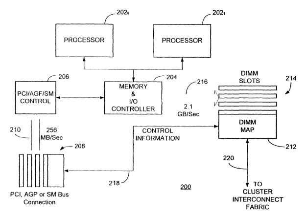
With reference additionally now to Fig. 5, a functional block
diagram of an exemplary embodiment of a computer system 200 in
accordance with the present invention is shown comprising a
switchlnetwork adapter port for clustered computers employing a chain of
multi-adaptive processors in a DIMM format to significantly enhance data
z0 transfer rates over that otherwise available from the peripheral
component interconnect ("PCI") bus.
In the particular embodiment illustrated, the computer system 200
includes one or more processors 2020 and 202 which are coupled to an
associated PC memory and I/O controller 204. In operation, the
controller 204 sends and receives control information from a PCI control
block 206. It should be noted that in alternative implementations of the
present invention, the control block 206 may also be an AGP or SM
control block. The PCI control block 206 is coupled to one or more PCI
card slots 208 by means of a relatively low bandwidth PCI bus 210 which
3o allows data transfers at a rate of substantially 256 MB/sec. In the
12
CA 02456179 2004-O1-28
WO 03/017118 PCT/US02/14574
alternative embodiments of the present invention mentioned above, the
card slots 208 may alternatively comprise accelerated graphics port
("AGP") or system maintenance ("SM") bus connections.
The controller 204 is also conventionally coupled to a number of
s DIMM slots 214 by means of a much higher bandwidth DIMM bus 216
capable of data transfer rates of substantially 2.1 GB/sec. or greater. In
accordance with a particular implementation of the present invention, a
DIMM MAP element 212 is associated with, or physically located within,
one of the DIMM slots 214. Control information to or from the DIMM MAP
to element 212 is provided by means of a connection 218 interconnecting
the PCI bus 210 and the DIMM MAP element 212. The DIMM MAP
element 212 then may be coupled to another clustered computer MAP
element by means of a cluster interconnect fabric connection 220
connected to the MAP chain ports. As previously noted, the DIMM MAP
i5 element 212 may also comprise a RIMM MAP element.
Since the DIMM memory located within the DIMM slots 214
comprises the primary storage location for the PC microprocessors)
2020, 202, it is designed to be electrically very "close" to the processor
bus and thus exhibit very low latency. As noted previously, it is not
ao uncommon for the latency associated with the DIMM to be on the order of
only 25% of that of the PCI bus 210. By, in essence, harnessing this
bandwidth as an interconnect between computer systems 200, greatly
increased cluster performance may be realized.
To this end, by placing the DIMM MAP element 212 in one of the
PC's DIMM slots 214, its FPGA 134 (Fig. 3) could accept the normal
memory "read" and "write" transactions and convert them to a format
used by an interconnect switch or network. As disclosed in the
aforementioned patents and patent applications, each MAP element 212
includes chain ports to enable it to be coupled to other MAP elements
30 212. Through the utilization of the chain port to connect to the external
13
CA 02456179 2004-O1-28
WO 03/017118 PCT/US02/14574
clustering fabric over connection 220, data packets can then be sent to
remote nodes where they can be received by an identical board. In this
particular application, the DIMM MAP element 212 would extract the data
from the packet and store it until needed by the receiving processor 202.
s This technique results in the provision of data transfer rates
several times higher than that of any currently available PC interface
such as the PCI bus 210. However, the electrical protocol of the DIMMs
is such that once the data arrives at the receiver, there is no way for a
DIMM module within the DIMM slots 214 to signal the microprocessor
1o 202 that it has arrived, and without this capability, the efforts of the
processors 202 would have to be synchronized through the use of a
continued polling of the DIMM MAP elements 212 to determine if data has
arrived. Such a technique would totally consume the microprocessor 202
and much of its bus bandwidth thus stalling all other bus agents.
To avoid this situation, the DIMM MAP element 212 may be further
provided with the connection 218 to allow it to communicate with the
existing PCI bus 210 which could then generate communications packets
and send them via the PCI bus 210 to the processor 202. Since these
packets would account for but a very small percentage of the total data
ao moved, the low bandwidth effects of the PCI bus 210 are minimized and
conventional PCI interrupt signals could also be utilized to inform the
processor 202 that data has arrived. In accordance with another
implementation of the present invention, the system maintenance ("SM")
bus (not shown) could also be used to signal the processor 202. The SM
z5 bus is a serial current mode bus that conventionally allows various
devices on the processor board to interrupt the processor 202. In an
alternative embodiment, the accelerated graphics port ("AGP") may also
be utilized to signal the processor 202.
With a DIMM MAP element 212 associated with what might be an
3o entire DIMM slot 214, the PC will allocate a large block of addresses,
14
CA 02456179 2004-O1-28
WO 03/017118 PCT/US02/14574
typically on the order of 1 GB, for use by the DIMM MAP element 212.
While some of these can be decoded as commands, (as disclosed in the
aforementioned patents and patent applications) many can still be used
as storage. By having at least as many address locations as the normal
s input/output ("I/O") block size used to transfer data from peripherals, the
conventional InteITM chip sets used in most PCs (including controller 204)
will allow direct I/O transfers into the DIMM MAP element 212. This then
allows data to arrive from, for example, a disk and to pass directly into a
DIMM MAP element 212. It then may be altered in any fashion desired,
~o packetized and transmitted to a remote node over connection 220.
Because both the disk's PCI bus 210 and the DIMM MAP element 212
and DIMM slots 214 are controlled by the PC memory controller 204, no
processor bus bandwidth is consumed by this transfer.
It should also be noted that in certain PCs, several DIMMs within
Zs the DIMM slots 214 may be interleaved to provide wider memory access
capability in order to increase memory bandwidth. In these systems, the
previously described technique may also be utilized concurrently in
several DIMM slots 214. Nevertheless, regardless of the particular
implementation chosen, the end result is a DIMM-based MAP element
zo 212 having one or more connections to the PCI bus 210 and an external
switch or network over connection 220 which results in many times the
performance of a PCI-based connection alone as well as the ability to
process data as it passes through the interconnect fabric.
While there have been described above the principles of the
25 present invention in conjunction with a specific computer architecture, it
is to be clearly understood that the foregoing description is made only by
way of example and not as a limitation to the scope of the invention.
Particularly, it is recognized that the teachings of the foregoing
disclosure will suggest other modifications to those persons skilled in the
3o relevant art. Such modifications may involve other features which are
already known per se and which may be used instead of or in addition to
CA 02456179 2004-O1-28
WO 03/017118 PCT/US02/14574
features already described herein. Although claims have been
formulated in this application to particular combinations of features, it
should be understood that the scope of the disclosure herein also
includes any novel feature or any novel combination of features
disclosed either explicitly or implicitly or any generalization or
modification thereof which would be apparent to persons skilled in the
relevant art, whether or not such relates to the same invention as
presently claimed in any claim and whether or not it mitigates any or all of
the same technical problems as confronted by the present invention. The
to applicants hereby reserve the right to formulate new claims to such
features and/or combinations of such features during the prosecution of
the present application or of any further application derived therefrom.
What is claimed is:
16