Note: Descriptions are shown in the official language in which they were submitted.
CA 02456218 2011-01-05
OPTICAL MODULATOR
BACKGROUND OF THE INVENTION
(1) Field of the Invention:
The present invention is related to an optical modulator, in particular an
optical modulator used as an optical intensity modulator, phase modulator, and
polarized wave modulator, for high-speed and high-capacity optical fiber
communications.
(2) Related art statement:
Recently, with the progress of high-speed and high-capacity optical fiber
communications, as represented by the exterior modulator, high-speed
modulators
using a substrate formed of a material having electro-optical effect, like
lithium
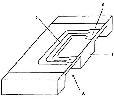
niobate, are in practical use. This high-speed modulator comprises substrate 1
formed of a material having electro-optical effect, with waveguide 2 that
guides the
optical wave, and modulate electrode comprising ground electrode 4 and signal
electrode 3 that applies the high-speed modulate signal in the microwave band
to
said optical wave, as shown in Fig.1.
To optical waveguide 2, an optical wave will enter from the end side of
optically polished substrate. When passing the optical waveguide 2, the phase
of the
optical wave will transform because of changing reflective index of the
substrate by
the electric signal applied to the electrode, and so, in the Mach-Zehnder
optical
modulator like Fig.1, phase transformation will perform the strength
modulation of
the optical wave. Then, the optical wave, which has been affected with the
strength
transformation according to the electric signal, will exit from the other end
of the
optical waveguide 2.
1
CA 02456218 2011-01-05
The electric connection of the signal electrode 3 and ground electrode 4 of
the
optical modulator is usually done from the side of the substrate because of
the
convenience of the wiring usage, and also electric signal connection pad 6 is
located
on the signal electrode 3 to connect the wiring from the coaxial cable.
Microwave, which is an electric signal, is provided from the coaxial cable, is
conveyed to the signal electrode 3 through the electric signal connection pad,
goes
thorough the bend point 7 of the signal electrode 3, and goes into the
interaction part
8 of the optical wave-guide 2. In these wiring, because of the rapid change of
the
electric property of electrical line, part of the micro wave as an electric
signal reflects
at the connecting point, other parts escape into the substrate, and other left
parts
radiate outside the substrate in consequence. For this reason, electric signal
which
transmits to the interaction part 8 of the signal electrode 3 decreases, and
effective
modulation to the optical wave which passes through the optical wave guide
becomes difficult.
Zb counteract this problem, efforts to reduce the loss of microwaves'
reflection and escape, by forming the signal electrode 3 and ground electrode
4 to be
as a co-planer type of plane electrode, connecting coaxial cable by impedance
matching, or easing the bend point of the signal electrode 3, have been tried,
but
effective reduction was difficult in the high frequency zone over 20 GHz.
The purpose of this invention is, to offer an optical modulator providing high
frequency broadband operation, which could effectively convey the electric
signal to
the interaction part of the optical wave-guide of the signal electrode, even
if the
electric signal exists in the high frequency zone.
2
CA 02456218 2011-01-05
SUMMARY OF THE INVENTION
In order to achieve the above-described purpose, the optical modulator, of
the instant invention comprises a single substrate formed of a material having
electro-optical effect, an optical waveguide formed on the substrate, and
electrode for
modulating light passing through the optical waveguide, with an electric
signal
connection pad unit provided on part of the electrode, and thickness of the
substrate
located on a lower part of at least the electric signal connection pad unit
and directly
or indirectly continuous to the electric signal connection pad unit, is
thinner than
thickness of another part of the substrate including an interaction part of
the
electrode by cutting off a part of the substrate, and is less than 250 tam.
In another aspect of this invention, by forming a channel on the side of the
substrate, the substrate located on a lower part of the electric signal
connection pad
unit and directly or indirectly continuous to the electric signal connection
pad unit, is
made thin.
In another aspect of this invention, the optical modulator is supported by a
chassis, and space is provided between a surface of the chassis and the
electric signal
connection pad unit on a lower part of the electric signal connection pad
unit.
In another aspect of this invention, material having electro-optical effect
forming the substrate is a material selected from the group consisting of
LiNbO3
crystal, LiTaO3 crystal, and solid solution crystal of LiNbO3 and LiTaO3.
In another aspect of this invention, the optical waveguide is a Mach-Zehnder
type waveguide having divergent waveguides, the thickness of the substrate
directly
or indirectly continuous to the electric signal connection pad unit is partly
thinner
than a remaining part of the substrate and said remaining part of said
substrate is
thinned so that a change of the whole thickness becomes practically
symmetrical
3
CA 02456218 2011-01-05
against a centerline of the divergent waveguides in Mach-Zehnder type
waveguide.
BRIEF DESCRIPTION OF THE DRAWINGS
Figure 1 is a simplified diagram of a known optical modulator.
Figure 2 shows the optical modulator with cutting off the part of the
substrates' rear
face.
Figure 3 is a graph showing the place to cut on the substrates' rear face of
the optical
modulator.
Figure 4 shows amount of microwave transmission attenuation versus frequency
in
the first example.
Figure 5 shows the optical modulator with a channel on the side of the
substrate.
Figure 6 is a graph showing the amount of microwave transmission attenuation
versus frequency in the first example.
Figure 7 shows the place to cut substrate for temperature characteristic
improvement.
Figure 8(a)-(d) are cross-sectional diagrams of respective optical modulators
shown
in Figure 3.
Figure 9(a)-(c) are cross-sectional diagram of respective optical modulators
shown in
Figure 7.
Figure 10 is a diagram showing the optical modulator of Figure 2 positioned on
a
chassis.
DETAILED DESCRIPTION OF THE INVENTION
The following is a detailed description of the present invention using a
favorable example.
4
CA 02456218 2011-01-05
The substrate forming the optical modulator is made of a material having
electro-optical effect, such as lithium niobate (LiNbO3 ; hereinafter referred
to as LN),
lithium tantalite (LiTaO), PLZT (lead lanthanum zirconate titanate), and
silica. In
particular, the substrate is constituted by the X cut board, Y cut board, and
Z cut
board of these single crystal materials. Especially, because of easy formation
as an
optical waveguide device, and because of having strong anisotropy, LiNbO3
crystal,
LiTa03 crystal, or solid solution crystal consisting of LiNbO3 and LiTa03, are
preferred. In the practical examples, lithium niobate (LN) is mainly used for
explanation.
There are methods to produce optical modulator, which use heat diffusing Ti
on LN substrate for forming a wave guide, and then form an electrode directly
on LN
substrate without setting up a buffer layer on a part or the whole of the
substrate, or,
that form an electrode indirectly with formation of a buffer layer as
dielectric Si02 on
the LN substrate to reduce the light transmission loss in the optical
waveguide, and
then form an electrode pattern of Ti or Au on it, and form a signal electrode
and a
ground electrode having a height of several tens pm by plating with gold.
In the present invention, an electric connection pad unit is formed directly
on a substrate without a buffer layer, or indirectly on a substrate by
providing a
buffer layer between the electric connection pad unit and substrate as
described
above.
Said buffer layer could be considered to be multi-layer structure by
providing films such as SiN or Si on top of the dielectric layer as Si02.
Generally, building plural optical modulators on one LN wafer and then
dividing the wafer into individual chips (individual optical modulators) will
yield an
optical modulator such as that prior art modulator shown in Figure 1.
CA 02456218 2011-01-05
In the present invention, by forming the following two structures in an
optical modulator such as that in Figure 1, improvement of high frequency
character
is made.
In the first example, by conducting a cut off process of the rear face of LN
substrate, the thickness of the part of the substrate is made thinner. And in
the
second example, via a cutting off process from the side of LN substrate, the
channel
part is formed.
In the first example, the rear face of the substrate having lmm thickness is
cuts off to make the thickness 200pm by method of sand-blasting or core-
drilling
( See Figure 2. Reference arrow A shows the cutting-off part).
Next, to conclude the optimum part at the cutting-off part, the
transformation of the frequency character between each cutting-off part was
investigated.
As the cutting-off parts, there were prepared: one in which only parts under
electric signal connection pad unit are cut off (element A. See Figure 3(a)),
one in
which parts under said pad and the bend point are cut off (element B. See
Figure
3(b)), one in which a part under said pad, bend point, and the interaction
part is cut
off (element C. See Figure 3(c)), one in which only a part under operating
point is cut
off (element D. See Figure 3(d)), and one in which no part is cut off (element
E).
In order to show respective cutting-off parts in Figure 3(a) to (d) more
clearly,
Figure 8(a) to (d) show cross-sectional diagrams of the optical modulator
along the
line X-X in Figure 3(a) to W. Figure 8(a) is the cross-sectional diagram of
Figure 3(a)
along the line X-X. 101 denotes a substrate; 102 an optical waveguide; 103 a
signal
electrode; 104 a ground electrode; 105 a buffer layer; and a part indicated by
the
arrow A is a cutting-off part. In a similar way, Figure 8(b) is the cross-
sectional
6
CA 02456218 2011-01-05
diagram of Figure 3(b); Figure 8(c) of Figure 3(c); and Figure 8(d) of Figure
3(d).
Figure 4 shows the result of measuring an amount of microwave
transmission attenuation against frequency regarding to each element A to E.
As the result shows, at the point over 25GHz, element A, B and C decreases
amount of the attenuation more than element D or E. And at the point over
40GHz,
element B and C shows more effect of decreasing amount of the attenuation.
Therefore, by making the thickness of the substrate under the electric signal
connection pad unit thinner than the other part of the substrate, preventing
the
reduction of microwave becomes possible. Especially by making the substrate
thinner at the area from the pad to the bend point of the signal electrode,
reducing at
a higher frequency band becomes possible.
Besides, if the thin part of the substrate is spread to the operating point
where the modulation of the optical wave that passes in the waveguide is done,
effect
at some level will be expected, but the thin part of the substrate will be
increased in
whole, mechanical strength of it will decline, and negative effect such as
breaking of
substrate may occur.
In the second example, as shown in Figure 5, channel B is formed by
processing with a dicing saw at the side of substrate 1 that also has 1mm
thickness.
For the method of process, one or more chips (modulator) are fixed by fixture
with the side of substrate up. Fixture has pressure parts made of Si on Si
base. The
fixing wax is applied between the chips and pressure parts, and the chips are
fixed
on Si base by pressure parts pushing the chips. Then by rotating the process
blade
with contacting the substrate side of chip, a channel with necessary depth and
length is formed to the side of substrate.
7
CA 02456218 2011-01-05
Next, related to the thickness of substrate formed the channel (thickness of
thin part), to search for the appropriate thickness of value d (figure 5),
frequency
character was investigated in the cases that vary the thickness d was varied
by the
difference of formulated location of channel.
For the sample, thickness d of the thin part with 150pm (element F),
200pm(element G), 250pm(element H), 300pm(element I), and one in which no
channel is formed (element J) were prepared. Width of the channel in all the
samples
was 300pm.
In Figure 6, the measurement result of the microwave transmission
attenuation amount against frequency related to each element F to J, is shown.
As the measurement result shows, for element F,G,H, over 25GHz, the
amount of attenuation is reduced drastically compared to element I and J
(since I
and J show almost the same level of frequency characteristic, they are shown
as the
same graph on Figure 6). As the thickness becomes thinner, the effect becomes
higher.
Therefore, by making the thickness of the part of the substrate that contains
the electro signal connection pad unit under about 250pm, control of the
attenuation
of microwave in high frequency becomes possible. By setting the thickness d of
the
substrate under about A/(10n) (X is the wavelength of microwave, n is
refractive
index of the substrate), control of the microwave radiation out of the
substrates will
be possible.
The width of the channel is set as 300pm in the example, but the present
invention is not limited by this. Generally, when the width becomes narrow,
the
phenomenon of microwave escape with passing the channel will occur and the
effect
to form a channel becomes weak. On the other hand, if the channel is too wide,
it
8
CA 02456218 2011-01-05
may cause cracking of substrate during processing with dicing saw. Therefore,
in the
permissible range of the effect, width of the channel could be appropriately
set.
In addition, channel length is composed as identical as the whole long way of
the optical modulator in the present example. However, from the perspective to
control the transport loss of microwave from the signal electrode, only in the
specific
zone that includes the electric signal connection pad unit and the bend point
of the
electrode, channel could be composed from the side of the substrate.
In addition, the optical modulator usually is fixed on a chassis made of brass
or stainless. Even if the thin part is formed in some part of the substrate by
processing the substrate, which forms the optical modulator, if the chassis
fills the
formed space, because the microwave could leak to the chassis side, the effect
that
was made by thinning the substrate could be reduced.
Therefore, there should be formed between the lower part of the electric
signal connection pad unit and the chassis, enough space up to the point that
would
not leak any microwave to the chassis.
Figure 10(a) is a diagram in which the optical modulator in Figure 2 is
positioned on a chassis 200 (a part of chassis). Figure 10(b) is a cross-
sectional
diagram of Figure 10(a) along the line X-X. 201 denotes a substrate; 202 an
optical
waveguide; 203 a signal electrode; 204 a ground electrode; and a part
indicated by
the arrow A is a cutting-off part. A space is formed between the substrate 201
and the
chassis by the cutting-off part under the electric signal connection pad unit
(right
end of 203) as shown in Figure 10(b).
In present invention, thickness of the part of the substrate located on or
continuous to the electric signal connection pad unit is thinner. To be more
precise, in
the cutting off process of the rear face of substrate as in Figure 3(a) to
(c), or the side
9
CA 02456218 2011-01-05
of the substrate as in Figure 5, only a part of the substrate is only cut off.
Therefore,
when the temperature of the substrate changes, the heat stress to each part of
the
substrate becomes unequal, and in consequence, the character of the optical
modulator will greatly depend on the temperature change. Especially, when the
heat
stress to light guide from the substrate's right and left across the wave-
guide differs
substantially, optical modulate character becomes unbalanced.
Therefore, in the Mach-Zender type wave-guide as shown in Figure 1, the
form of the substrate is desirable to form actual symmetry against the
centerline of
the divergent waveguides in the Mach-Zender type waveguide. To be more
precise,
as in the oblique lined parts of Figure 7(a) to (c), by cutting off the
substrate so that it
becomes symmetrical against the centerline between the divergent waveguides
(in
Figure 7(a) to 7(c), shown as "centerline of waveguide ".) , the heat stress
to the
waveguide becomes equal in both sides.
In order to show respective cutting-off parts in Figure 7(a) to (c) more
clearly,
Figure 9(a) to (c) respectively show cross-sectional diagrams of Figure 7(a)
to (c).
Figure 9(a) is the cross-sectional diagram of Figure 7(a) along the line X-X.
101
denotes a substrate; 102 an optical waveguide; 103 a signal electrode; 104 a
ground
electrode; 105 a buffer layer; and a part indicated by the arrow A is a
cutting-off part.
In a similar way, Figure 9(b) is the cross-sectional diagram of Figure 7(b);
and Figure
9(c) is the cross-sectional diagram of Figure 7(c).
INDUSTRIAL APPLICABILITY
As described above, according to the optical modulator of the instant
invention, the thickness of the substrate that located on a lower part of at
least the
electric signal connection pad unit, and continuous to it, is made thin,
controlling the
CA 02456218 2011-01-05
cause of leakage inside the substrate and escape outside the substrate of the
microwave in said pad area, and yielding an optical modulator which enables
safe
operation even in the high frequency broadband.
According to another aspect of the invention, since the thickness of a part of
the substrate under the electrical signal connection pad unit is under about
250pm,
stable operation could be possible even if it is in high frequency broadband
over
25GHz.
According to another aspect of the invention, by forming a channel on the
side of the substrate, because a part of the substrate under the electric
signal
connection pad unit is formed more thinly, the processing method will be easy
and
making accurate thickness of the thin part on the substrate will be possible,
compared to the method of forming the substrate thinly from the rear face of
the
substrate by sandblasting.
According to another aspect of the invention, because a space between the
chassis which holds the optical modulator and the electric signal connection
pad unit
is formed, prevention of microwave leak to the chassis side will be possible,
yielding
an optical modulator that can better control the reduction of microwave.
According to another aspect of the invention, because the substrate formed
of the material having electro-optical effect is made of either LiNbO3
crystal, LUTaO3
crystal, or solid solution crystal of LiNbO3 and LiTa03, it can yield an
optical
modulator that is suitable to high-speed reply, and if this feature is added,
it is
possible to gain an optical modulator that is available to use for higher
frequency
broadband.
According to another aspect of the invention, the heat stress to the optical
wave guide will be symmetrical, for thickness alteration of the whole
substrate is
11
CA 02456218 2011-01-05
under control so that it will be actually symmetrical against the centerline
of the
divergent waveguides in the Mach-Zender type optical waveguide, enabling
control
of the phenomenon of the optical modulator characteristic depending on
temperature change.
12