Note: Descriptions are shown in the official language in which they were submitted.
CA 02456234 2004-02-02
WO 03/012531 PCT/US02/24540
-1-
TUNABLE OPTICAL INSTRUMENTS
BACKGROUND OF THE INVENTION
Tunable optical instruments are a class of instruments in which a property of
light, such
as power level, is measured at more than one wavelength. Such instruments
include optical
spectrum analyzers (OSAs), optical channel monitors (OCMs) and others used in
the wavelength
division multiplexed (WDM) optical communication field, as well~as other
fields.
An OSA is a piece of equipment or a measurement instrument that receives an
optical
input and produces an output that represents the optical power contained in
the optical input over
a range of wavelengths. When we use the term "optical," we mean to refer to a
band of
wavelengths of electromagnetic radiation including at least visible light,
ultraviolet (UV) and
infrared (IR). The teen should be viewed inclusively, particularly when an
application of the
described technology overlaps one of the explicitly named bands and also
includes wavelengths
marginally outside those bands.
Lilce all inshuments realized in the "real world," OSAs have a finite
resolution
determined by characteristics of the components of which they are constructed.
However,
spectrum analysis is generally thought of as producing a continuous
representation of the power
distribution across the measured band. That is, the power at each wavelength
within the
measured band is represented, even though resolution limits may mean that the
represented
power actually includes some power from nearby wavelengths, as well.
In some optical communication systems, plural channels of information may be
transmitted on a single medium by modulating each channel onto a carrier
having a different
wavelength. Such systems include wavelength division multiplexed (WDM)
systems. An
instrument adapted to measure optical power at the specific, discrete channel
carrier
wavelengths is an OCM. Of particular, but not exclusive, interest to us are
WDM systems
operating with channel carrier wavelengths around 1500 nm.
Conventional OSAs and OCMs are bulky and expensive because the tunable filters
used
employ mechanical tuning means, such as moving a grating, stretching a fiber,
etc. Such
systems are also slow to time, often requiring seconds,to tune just a few
nanometers in
wavelength.
SUMMARY OF THE INVENTION
According to aspects of embodiments of the invention, there are provided
several
systems and variations thereon.
An optical instrument may include a tunable free-space filter as a wavelength
selector. A
free-space filter is defined as one for which light is propagated normal to
the planar surface of
CA 02456234 2004-02-02
WO 03/012531 PCT/US02/24540
_2_
the filter in the form of a beam, as contrasted with devices that guide light
in waveguides or
fibers. The optical instrument may be an optical spectrum analyzer (OSA).
Indeed, the OSA
may be constructed and arranged as an optical channel monitor for wavelength-
division
multiplexed optical communication systems.
According to some variations, the tunable free-space filter is a tunable thin
film filter
(TTFF). The TTFF may be thermo-optically tunable. The tunable filter may be a
mufti-layer
film structure incorporating thin film semiconductor materials. The
temperature, and hence the
wavelength, of the TTFF may be varied using an external thermal energy
transfer device. The
thermal energy transfer device may be a resistive heating device. The
resistive heating device
may be a ring-shaped metallic film, defining an aperture through which light
passes through the
filter. The resistive heating device may alternatively be an optically
transparent layer that is
integrated with the filter in a location such that light passes through the
resistive heating device.
In one set of variants, the transparent layer may be a transparent conducting
oxide.
Alternatively, the transparent layer may be a doped thin film selected from
the list including
amorphous, micro-crystalline, and polycrystalline semiconductor films, or it
may be a doped
crystalline semiconductor.
Various TTFF structures are possible. The TTFF may have a single-cavity Fabry-
Perot
structure or may have a mufti-cavity structure.
Packaging variants can be made. For example, the TTFF and the optical detector
can be
mounted in a single hermetic package. The single hermetic pacleage may be a TO-
style package.
Within the single hermetic package may be one or more discrete temperature
sensors. Also,
within the single hermetic package may be one or more temperature-stabilizing
devices.
Several calibration aids can be included. The optical instrument may further
include an
external source of one or more known wavelength signals. Alternatively, the
instrument may
include an internal source of one or more known wavelength signals. In yet
another alternative,
the instrument may fiu-ther comprise passive interferometric structures within
the optical
instrument that create a stable wavelength reference. In this alternative, the
interferometric
structures may include a substrate of the tunable flee-space filter. The
interferometric structure
may interact with a known light source to establish a reference signal.
The optical instrument may further include a device that measures temperature
of the
thermo-optically tunable TTFF to determine wavelength. The device that
measures the
temperature may be integrated with the TTFF. The TTFF may further include a
heater layer. In
that case, the heater layer may further include the device that measures the
temperature. For
example, the device that measures the temperature may monitor resistance of
the heater layer.
In one variant where the device that measures the temperature monitors the
resistance of the
CA 02456234 2004-02-02
WO 03/012531 PCT/US02/24540
-3-
heater layer, there is a source of a DC current to heat the heater layer and a
source of a
superposed AC current that is sufficient to monitor resistance of the heater
layer.
The optical instrument may fiu~ther comprise a detector having an output and a
signal
processor connected to receive a signal from the detector output, the signal
processor converting
the signal received from the detector output to power v. wavelength data.
In yet another packaging variant, the optical instrument may include an
electronics
module; an optical detector; a fiber optic input; and a transistor outline
(TO) package into which
are mounted the tunable free-space filter, the optical detector and the fiber
optic input, the TO
package including pins through which electrical connections between the
tunable free-space
filter and the optical detector, and the electronics module are made. In this
instance, the
instrument may further include a single enclosure supporting the TO package
and the electronics
module.
BRIEF DESCRIPTION OF THE DRAWINGS
In the drawings in which like reference designations indicate like elements:
Fig. 1 is a schematic block diagram of an optical instrument including a TTFF;
Fig. 2 is a block diagram of the instrument of Fig. l, further detailing
signal processing
aspects thereof;
Fig. 3 is a plan view of a tunable Fabry-Perot filter having a ring heater;
Fig. 4 is a schematic cross section view of the filter of Fig. 3;
Fig. 5 is a schematic cross section view of a filter having a bottom heater;
Fig. 6 is a schematic cross section view of a filter having a top heater;
Fig. 7 is a schematic cross section view of a filter having a bottom
crystalline
semiconductor heater;
Fig. 8 is a schematic cross section view of a filter having both a top heater
and a bottom
heater in the same filter structure;
Fig. 9 is a schematic cross section view of a filter in which the spacer layer
also serves as
the heater;
Fig. 10 is a graph of dn/dT comparing a Site alloy having superior thermo-
optic
characteristics to Si;
Fig. 11 is a graph of dn/ndT comparing the Site alloy and Si materials whose
properties
are shown in Fig. 10;
Fig. 12 is a graph of transmittance v. wavelength comparing a Fabry-Perot
filter nominal
design to the filter with up to 0.5% thickness errors in the deposition of the
layers;
Fig. 13 is a graph of transmittance v. wavelength comparing a Fabry-Perot
filter nominal
CA 02456234 2004-02-02
WO 03/012531 PCT/US02/24540
-4-
design with no absorption in the spacer to the filter with an absorption
coefficient, k=0.001;
Fig. 14 is a graph of transmittance v. wavelength comparing a Fabry-Perot
filter
receiving a collimated light beam to the filter receiving light from a single
mode fiber without
collimation;
Fig. 15 is a graph of transmittance v. wavelength comparing a Fabry-Perot
filter nominal
design to the filter with a higher contrast ratio between refraction indices
of the mirror layers;
Fig. 16 is a graph of transmittance v. wavelength comparing the tuning range
of a Fabry-
Perot filter nominal design to the filter with a thicker spacer layer;
Fig. 17 is a graph of transmittance v. wavelength comparing the tuning range
of a Fabry-
Perot filter with only the spacer having thermo-optic properties to the filter
with the spacer and
the high index mirror layers having thermo-optic properties and to the filter
with all layers
having thermo-optic properties;
Fig. 18 is a graph of field intensity overlaid on a cross section view of a
combined TTFF
and resonant cavity enhanced detector;
Fig. 19 is a side view of a chip carrier used to package a TTFF;
Fig. 20 is a top view of the chip carrier of Fig. 19;
Fig. 21 is a cross section view of a transistor outline (TO) package into
which the chip
carrier of Figs. 19 and 20 has been mounted;
Fig. 22 is a cross section view of a TO package similar to that of Fig. 21,
but into which
a thermo-electric cooler has been also mounted;
Fig. 23 is a cross section view of a complete optical instrument package;
Fig. 24 is a cross section view of a thin film stack incorporating a
resonantly enhanced
PIN detector and a TTFF;
Fig. 25 is a cross section view of a TO package showing a fiber connection
through the
top;
Fig. 26 is a perspective view of three TO packages having different fiber
connection
ports in the tops thereof;
Fig. 27 is a perspective view of a dual in line pin (DIP) package with an
optical port in
the top thereof;
Fig. 28 is a perspective exploded view of a mask alignment system for
assembling an
optical component;
Fig. 29 is a perspective exploded view of a surface mount technology (SMT)
alignment
system for assembling an optical component;
Fig. 30 is a perspective exploded view of an intermediate mask alignment
system for
assembling an optical component;
CA 02456234 2004-02-02
WO 03/012531 PCT/US02/24540
-5-
Fig. 31 is a perspective view showing multiple die assembly in a large sheet;
Fig. 32 is a perspective view showing a separated die from the sheet shown in
Fig. 31;
Fig. 33 is a cross section view of an optical assembly including an external
dual fiber
collimator used to introduce light into the package and to receive light
rejected by the filter in
the assembly;
Fig. 34 is a cross section view of an optical assembly including a bare fiber
that
introduces light through a collimating lens and diffraction grating that
directs light onto an array
of filters and detectors;
Fig. 35 is a cross section view of a TO package with a ferrule to receive a
fiber;
Fig. 36 is a cross section view of a TO package with a direct mount in the cap
for
receiving a fiber;
Fig. 37 is a perspective view of a TO header to which an optical component has
been
mounted and bonded for electrical connection; and
Fig. 38 is a top view of a filter heater with a four-point contact
arrangement.
DETAILED DESCRIPTION
The present invention will be better understood upon reading the following
detailed
description of various aspect of embodiments thereof in connection with the
figures.
Tunable thin film filters (TTFFs) are free-space filters that admit beams of
light, for
example collimated light, and filter out specific wavelength or sets of
wavelengths for
transmission or reflection. The optical beams to be filtered are unguided
except for input and
output optics which extract them and insert them into waveguides such as
optical fibers.
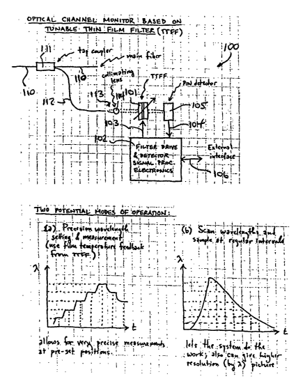
A block diagram of an optical instrument 100 including a TTFF 101, such as an
OSA or
OC1VI is shown in Fig. 1. The TTFF 101 comprises semiconductor thin films
possessing large
thermo-optic coefficients leading to wide tunability with no moving parts.
Integral with or
closely associated with the TTFF 101 are devices for heating and/or cooling
the filter over a
wide temperature range. A signal-carrying optical fiber 110 passes through a
top coupler 111.
Some of the signal is carried in fiber 112 to the instrument 100. The signal
exits the fiber at 113
to pass through a collimating lens 114 to TTFF 101. The control electronics
102 sweep the
TTFF 101 through a range of wavelengths by controlling the current drive 103
to a resistive
heater. The TTFF 1 O1 can alternatively be tuned to a specific wavelength.
Either during the
wavelength sweep, or when the TTFF wavelength has stabilized, depending on the
type of
measurement, a photocurrent 104 from a PIN detector 105 is read. The resulting
information is
processed as appropriate, and then the system conveys the resulting spectrum
or measurement to
the outside world 106. In an OSA application, the result is a table of power
measurements over
CA 02456234 2004-02-02
WO 03/012531 PCT/US02/24540
-6-
the continuous range of wavelengths through which the TTFF has been swept. In
a simple OCM
application, the result communicated is a "channel power table" which is
simply a list of power
measurements at each of the discrete carrier wavelengths or channels in use or
available in an
optical communication system.
The internal functions of OSAs and OCMs have been described in multiple
previous
patents and publications. We will focus on those aspects that are specific to
the use of a TTFF
in such instruments.
As one example, an embodiment of an OSA or OCM built using the TTFF is shown
in
Fig. 2. An analog circuit 201 periodically drives the tunable thin film heater
with a pulse of
current 202 that rapidly heats the filter 101, thereby shifting its
transmission to a wavelength
beyond the range to be scanned. Either during the heating pulse or as the TTFF
cools, an
analog-to-digital converter 203 samples alternately the PIN photodiode 204
output and a signal
from a film temperature measurement circuit 205 that represents the
temperature of the active
film. The PIN photodiode 204 output may be amplified, for example by log
amplifier 206. A
multiplexes 207 selects between the PIN photodiode output and the temperature
measurement
output. Once converted to tile digital domain, the results are fed to a
microprocessor or digital
signal processor 208. DSPs are available with built-in A/D converters and full-
function
interfaces thus integrating into one component several of the functions just
described. The
signal is then processed to produce the output spectrum or carrier table, as
described above.
Finally, the results are communicated to the host system through a standard
serial interface 209.
Next, we discuss producing and measuring the temperature swing described
above, as well as controlling the temperature of a thermally tunable filter.
The quality of the
temperature control scheme will ultimately determine many performance
parameters of the
filter, including tuning speed, tuning range, peals width, and power
consumption. When
choosing a temperature control method, heating and cooling speed and
efficiency, temperature
uniformity, and material properties all need to be considered.
Heating and cooling elements for a thin-film filter can be classified into
three categories
based on their proximity to the active layer. The first category includes
heating/cooling
elements external to the device, thermally coupled to its substrate or
package. A second
category includes heating or cooling elements integrated into the device,
providing more
efficient thermal control due to the increased proximity to the active layer.
The third, highly
efficient, thermal design uses the active layer itself as the heating or
cooling element.
An external temperature controller is one simple way to control the
temperature of a
thermally tunable device. For example, the filter can be mounted on a feedback-
controlled
thermo-electric (T/E) heater/cooler. This approach is simple but has many
disadvantages. First,
CA 02456234 2004-02-02
WO 03/012531 PCT/US02/24540
_7_
a T/E heater/cooler has a limited temperature range - translating into limited
tuning range, and is
relatively slow to perform large temperature swings, on the order of seconds
to tune through a
complete range, thus defeating one of the advantages of TTFFs, namely their
small thermal
mass.. Also, because the T/E element is external to the device itself, the
substrate and the
package will be heating and cooled along with the device. This contributes to
relatively large
power consumption and slower temperate r a control and tuning speed by
increasing the thermal
mass of the system.
To solve these problems, a resistive heating element can be integrated
directly with the
filter. One embodiment of a tunable thin-film Fabry-Perot filter is shown in
Fig. 3. Metal pads
301 make electrical contact to a thin-film metallic ring-shaped resistor 302,
which heats the filter
300. In the cr oss-sectional view of Fig. 4, 401 indicates the dielectric thin-
film mirror stacks of
a Fabry-Perot filter. The Fabry-Perot cavity layer 402 is the thermally
tunable material.
By running a current through the resistive heater 302 using contact pads 301,
resistive
heat is generated, which will change the optical properties of the cavity
layer 402, as well as
other layers, and thus tune the filter 300. Light travels perpendicular to the
page in Fig. 3,
through the hole 303 at the center of the resistive heater, the active filter
area. This type of
heater could be made of any suitable material capable of carrying enough
current to generate the
necessary resistive heat. For example, a ring-shaped heater 302 with a 300
micron diameter, 50
microns wide, leaving a 200 micron aperture 303, made of a 100nm thick film of
chromium
would have a resistance of approximately 10 Ohm. The power dissipated by such
a resistive
heater is given by P=IZR. Assuming 1 mW is needed to heat the filter
sufficiently to have the
desired tuning range, a voltage of 3.2 V across the heating element would be
generate 0.32 mA
and 1 mW of power. This device can be mounted on a heat sink attached to a T/E
cooler held at
a constant, low temperature, which would provide cooling. Thus, using the
pulse drive noted
above, a temperature sawtooth, and hence a wavelength sawtooth, results.
This method of heating is more efficient than the external heater described
above
because the heating element is in closer proximity to the active layer. This
will lead to faster
heating and tuning, and less power consumption. Also, a heating element of
this type has no
temperature range independent of the operating temperature limits of the
material of the TTFF
and the conductive ring, itself. However, the disadvantage of this
configuration is poor
temperature uniformity across the active filter's area because heat must be
transferred from the
inner edge of the heater to the center of the active filter area. This non-
uniform temperature
distribution will lead to a broad or distorted transmission peak because the
beam occupies a
finite, non-zero area of the active filter area, and therefore will be
distributed across a range of
different filter properties corresponding to different local temperatures.
CA 02456234 2004-02-02
WO 03/012531 PCT/US02/24540
-8-
According to another arrangement, a thin-film resistive heater is made
transparent to the
wavelengths of interest. In this case, it could be positioned in the path of
the light, providing
more uniform heating. FIG. 5 shows a tunable thin-film Fabry-Perot 501 filter
with this type of
heating element 502 integrated between the substrate 503 and filter stack 504.
Such a heating
element 502 could alternatively be one of the mirror stack layers 505 or even
the Fabry-Perot
cavity layer 506, if such are arranged to be both transparent to the
wavelength of use and also
sufficiently conductive. While the films currently in use for filters in the
wavelength division
multiplying (WDM) industry are primarily dielectrics, an advantage of our
semiconductor thin
films is that they combine good optical properties and low loss with desired
thermo-optic
properties and good conductivity when suitably doped. A heating element 502 of
this type for
application in the telecommunications industry could be made of one of several
transparent
conductors, such as zinc oxide, indium tin oxide, a doped thin film of
amorphous, micro-
crystalline, or poly-crystalline semiconductor, etc. Poly-silicon films,
formed by re-crystallizing
in an oven films deposited as amorphous silicon, are especially adaptable to
this purpose.
Because these transparent conductors have higher resistivities than most pure
metals, the heating
element should be made as small as possible to maximize the resistive power
density.
One other possible material for a semi-transparent resistive heater is a doped
crystalline
silicon or some other semiconductor crystal. In this case, the filter
substrate would be the
crystalline semiconductor wafer, and the filter would be fabricated on top of
a doped area. Of
course, the semiconductor both intrinsic and doped, must be transparent to the
wavelengths of
interest.
The doped semiconductor, and the thin-film transparent resistive heaters both
greatly
improve the temperature uniformity across the filter over the ring-shaped
resistive heater
described above. Also, the filter and heater combination can be made smaller
leading to lower
power consumption and a small device footprint.
Fig. 6 shows the heating element 601 integrated on top of the filter stack
602. FIG. 7
shows a filter 700 fabricated on top of a doped area 701 of a crystalline
semiconductor. The
doped area 701 forms a heater element. FIG. 8 shows a filter 801 with a
transparent thin-film
resistive heating element fabricated on the top 802 and the bottom 803 of the
filter stack 804.
' An advantage of having two heating elements is double the heating
capability. Also, one
of the elements could be used as a thermometer provided it is made of a
material whose
resistance is a function of temperature. The choice of configuration depends
on the specific
application requirements.
All the integrated resistive heating element designs considered above have the
advantages of uniform temperature distribution over the filter area,
relatively close proximity to
CA 02456234 2004-02-02
WO 03/012531 PCT/US02/24540
the tunable layer, and no inherent temperature limit. However, because the
heating element is in
the path of the light, it may absorb or scatter light leading to a smaller
transmission peals and a
higher insertion loss of the filter. Also, many of the transparent conducting
oxides that might be
used for this purpose are not stable with temperature. Finally, these
configurations are not the
most efficient ways to heat the tunable layer. For example, for the
configuration shown in Fig.
5, much of the heat generated by the heating element 502 is lost to the
substrate 503 instead of
going directly to the tunable layer 506.
The most efficient way to heat the tunable layer is to use the layer itself as
the heating
element, as briefly noted above, provided it is electrically conductive, for
example a doped
semiconductor thin film. Fig. 9 shows a tunable Fabry-Perot filter 900 with
electrical contact
301 directly to the tunable layer 901, which is used as a resistive heater in
the same way as
described above for the integrated heater. Of course in this case, the tunable
layer 901 must
have a low enough resistivity to be able to carry enough current to generate
the necessary
resistive heat, in addition to meeting all the optical requirements of a Fabry-
Perot cavity layer.
This configuration involves the fewest compromises in terms of the heater and
tuning
performance. Since the tunable layer itself is the heating element, no more
efficient heating of
that layer is possible, meaning the fastest tuning time and lowest power
consumption. Also, as
with the transparent integrated heating elements described above, relatively
uniform heating can
be achieved. Lastly with this configuration, no additional layers are in the
path of the light
traveling through the Fabry-Perot filter. Therefore there will be no
umiecessary loss or
modification to the optical signal. For a spacer having an index of 3.5,
tuning over 30 nm in the
1500 nm band requires a temperature change of more than 350 C. Such a large
local heating is
achieved in om embodiments by a combination of concentrated electrical power
dissipation in a
microscopic volume, extremely strong film adhesion and materials where
properties are stable
under repeated cycling.
Consider now a spacer material with a thermo-optic coefficient dn/dT = 2x1 0
~/°C used
in the above-described structure.
To get a sense of the materials properties requirements, we let the length L
and width W
of the heater element be L=W=1 mm and set the operation voltage to be IOV. The
power
density is P/WL=I2R/WL = V2/RWL, and should be about 1 W/cm2. Therefore the
target heater
film resistance R must be about 10I~ ohm. For a thin film heater layer
thickness d=100nm and
W/L=1, then the target resistivity of the heater material needs to be
RdW/L=0.1 ohm-cm.
Materials that can be used for the heater must have not only low optical
absorption at the
wavelengths of interest (~1550nm) belt must also have low electrical
resistivity in order to
provide high enough electrical current at the operating voltages to generate
sufficient heat to the
CA 02456234 2004-02-02
WO 03/012531 PCT/US02/24540
-10-
filter (spacer layer). Materials which can satisfy these requirements include
but are not limited
to polycrystalline, microcrystalline or nanocrystalline silicon, indium tin
oxide and zinc oxide.
To optimize heater operation, note that power density = Vad /rho L2. That is,
power density
goes as square of (V/L) but only linearly with thickness d.
As mentioned above, one method of driving the heater, based on the TTFF's
thermal
architecture involves supplying a current spike to the filter heater layer-
which heats the filter
very rapidly - and make measurements during the cooling process. In an analog
circuit, the
current spike could simply be the result of a capacitor discharge. With the
proper thermal and
electrical design, a relatively linear curve can be achieved.
According to a second method, the filter is set to a specific wavelength,
stabilized at this
wavelength, and then a measurement is taken. This allows for very high
accuracy at a specific
wavelength, assuming the wavelength can be locked well.
Several methods may be used to measure wavelength as the scan or wavelength
setting
occurs, regardless of the method by which the scan or wavelength setting is
performed. Several
are now described.
Pre-calibrated curves defining a steady temperature vs. time profile are used
in one
method to estimate wavelength being transmitted by the filter. If the TTFF is
in a temperature
stabilized environment, no additional measurement or computation is required,
since it may be
assumed that the temperature vs. time profile remains constant over the OCM's
operational life.
however, if the TTFF is not temperature stabilized, the temperature vs. time
scan profile will
likely change. The addition of a thernistor to measure TTFF assembly
temperature and a series
of calibrations at different ambient temperatures allows a reasonable estimate
of wavelength vs.
time to be obtained.
According to another method, the TTFF temperature can be directly measured
using
temperature-dependent thin film resistors (thernistors) that are integrated
with the device. Since
wavelength is directly related to temperature in the TTFF, such a measurement
gives a very
good instantaneous estimate of transmitted wavelength. In order to produce a
result that
correlates well with the filtered wavelength, measuring the temperature of the
device should be
done accurately and should be localized to the place where the light goes
through the device,
which is a small portion of the device area. Three possible configurations are
now described.
The thin film heating element in the TTFF can be used as both the heater and
the
temperature monitor. To implement this, a small amount of current should be
run continuously
into the film and the voltage over the film measured. The relationship between
current and
voltage may be monitored to determine film resistance, and therefore,
temperature. One
potentially superior way of providing these measurements is to superimpose a
small AC signal
CA 02456234 2004-02-02
WO 03/012531 PCT/US02/24540
-11-
over the heating current, at a frequency sufficiently high relative to the
TTFF's thermal time
constant such that it essentially results in very small DC heating, and
measure resistance directly
in this manner. A simple analog circuit could be constructed to provide this
function and not
interfere with TTFF operation. It would provide a single analog output that is
a function of the
heater's resistance, representing temperahire, that would in turn be used to
determine filter
wavelength.
Because, in some configurations, the temperature of the heater film may not
accurately
represent the overall temperature of the filter, particularly if it is on one
side of the TTFF, it may
be preferable to insert another thermistor layer into the structure which
better reflects active
layer temperature. Such a layer may be made of very similar materials to the
heater, for
example, ZnO, polycrystalline silicon, bulk crystalline silicon, thin metal
lines, and many others,
and may be measured in much the same manner as described above, including the
AC signal. It
should be noted that the ideal layer for both temperature measurement and
heating is the cavity
layer in the TTFF. Even if the materials constraints do not allow for direct
heating of the spacer
layer, it would be highly advantageous to use this layer as a thermistor,
which can be done even
with highly resistive materials, given the correct circuit, in order to get
very accurate wavelength
determination.
For even more accurate temperature measurement, both the heater layer and
another
layer in the film, preferably placed on the opposite side of the spacer from
the heating layer,
should be used. The combined measurements of these films together with a
simple model for
thermal flux will give very accurate numbers for spacer film temperature and
therefore
transmitted wavelength.
The most accurate method of determining wavelength is to measure it optically
using
calibration methods. At least three possible methods axe now described.
The fiber optic network system which is the target of the OCM can be
configured to
contain calibrated optic signals at reference wavelengths which may be
monitored by the OCM.
Preferably, there are at least two such reference wavelengths so as to provide
"end markers" on
each bound of the band. However, this approach has not presently been adopted
in commercial
communications equipment and so it cannot be relied upon.
A stable wavelength reference source can be built into the OSA or OCM. Many
OCMs
and optical spectrum analyzers indeed take this approach. An LED, which has a
relatively
broadband emission, together with a filter, for example a stabilized Fabry-
Perot etalon, are used
to create a wavelength reference. The advantage is a stable, absolute
reference. The
disadvantages include more expensive components and packaging, additional
reliability
concerns, and expanded pacleaging size.
CA 02456234 2004-02-02
WO 03/012531 PCT/US02/24540
-12-
Because heat is dissipated through the thermally conductive contact pads and
substrate,
the temperature across the entire heater using either of the first two
approaches is not uniform.
'Thus the temperature measured by one of these two-point methods does not
accurately
correspond to the temperature at the spatial position at which light is
transmitted. A solution, as
shown in Fig. 38, is to use foul', instead of two, electrical contacts, i.e. a
four-point probe to
measure only the center resistance during heating. Heater 3801 is supplied
with heater current
through contacts 3802. Two tiny probes 3803 extend to points 3804, 3805 on
opposite edges of
the heater film 3801, near the center, so as to measure only the center
resistance during
operation. The conductor forming these traces 3803 has to be thin so that it
does not itself affect
temperature uniformity.
According to a third approach, an additional optical element in the light path
can be used
to create regular, fixed disturbances in the transmission spectrum. For
example, a Fabry-Perot
cavity with relatively weak mirrors and a cavity large compared to the
wavelength will have this
effect of creating a "ripple" on top of the incoming transmitted light.
Because it is a fixed
pattern with a known effect, this ripple may be easily separated out of the
overall signal received
during wavelength scan. The signal may then be used as a "scale" for the true
signal data that
was gathered during the scan, both on a relative and absolute scale. Such a
cavity and function
may be easily integrated into the TTFF. The substrate on which the filter is
constructed may in
fact serve as a Fabry-Perot cavity for this purpose. It will be temperature
stabilized, at least for
high-resolution applications where such a scale is really necessary. On the
electronic side, this
"pilot tone" could be picked up by an analog circuit to measure the "rate of
aseent/descent" in
wavelength during a scan. Note that this method of wavelength referencing may
be applied not
only to the TTFF, but to other types of tunable filters as well.
In short, there are many ways to estimate wavelength for each detector data
point
collected, ranging from a one-time calibration in the factory to continuous
optical signal
monitoring. Several of these methods lend themselves to low-cost
implementation in the TTFF-
based OCM package.
VJe now turn our attention to a more detailed discussion of materials As
previously
mentioned, materials suitable for the embodiments described herein should
possess a
combination of excellent transparency at the wavelengths of use, large thermo-
optic coefficients,
low scattering, high adhesion both between layers and between the stack and
the substrate,
compatible coefficients of thermal expansion and stable properties over
repeated temperature
cycling by several hundred degrees Celsius over a long service life. Also, the
materials should
be formed and deposited with accurate, uniform thickness and properties.
Plasma enhanced
chemical vapor deposition (PECVI~) is useful for depositing layers of
hydrogenated amorphous
CA 02456234 2004-02-02
WO 03/012531 PCT/US02/24540
-13-
silicon (a-Si:H) and related materials as thin film filters. While any
material suitable for making
a Fabry-Perot filter or other structure, and having a useful thermo-optic
coefficient could be
used, we now describe the a-Si H and related materials as suitable examples.
It is desir able to control the index of refraction of the various films, in
addition to their
physical, and thus optical, thicknesses. PECVD is a well-established technique
for deposition of
thin films of semiconductors and dielectrics such as Si02, a-Si:H, and a-SiNX.
Many filters,
including the Fabry-Perot thin film filters discussed above include
alternating layers of high and
low index material. Others use a continuously varying index to make a rugate
filter (see Applied
Optics 25 (16), p. 2644 (1986) by P. Baumeister). Making other of these
structures requires
having control over the index and thickness of the various materials used.
The low refractive index of a-SiN,; and the relatively high index of a-Si:H,
1.77-2.05
depending on gas mixtures and 3.62 at 1.55pm, respectively, in our process,
can be used to make
mirrors with reflection bands centered on 1550nm. All layers of the mirror
portions of the film
stack are one quarter wave optical path length, that is nd=~,/4. In the spacer
layer, we use
a-Si:H, with its high thermo-optic coefficient with an optical thickness of a
half wave or a
multiple thereof resulting in a thermally tunable filter. Thus, only two
compatible materials are
used. By varying the refractive indices of these materials, for instance
slowly changing the
composition of the a-SiN~ to a-Si:H (in the PECVD process, decreasing the
ratio of the flow of
NH3 to SiH4) we can alter the index from 1.77 to 3.62 in a quasi-continuous
fashion.
Furthermore, by adding GeH4 to the gas mixture in the plasma, we may increase
the index of the
spacer layer and of the high index layers of the mirror stacks to 4.2.
Increasing beyond this
point does not improve the filter performance further because the a-SiCe:H
starts to absorb more
strongly beyond a certain fraction of Ge. Thus, by varying the plasma
chemistry and deposition
parameters, we are able to control very well the refractive index and the
thickness of these thin
films.
Materials for the heater layer are now discussed. The heater material should
be a
material which is compatible with the other materials mentioned including the
thermal budget
and chemical processing associated with their production, and which can be
used as a heater.
Presently preferred is to use a conductive thin film of the proper index which
serves
simultaneously as an optical layer of the filter and also as the resistive
heater. Therefore the
material should not scatter or absorb the light, should have a proper index of
refraction, and
must have a conductivity large enough that running current through it will not
require a very
large voltage. Several potential candidates exist, the leader of which is
polycrystalline silicon.
Others include transparent CollduCtlllg oxides, degenerately doped wide-gap
semiconductors and
doped micro- or nano- crystalline silicon.
CA 02456234 2004-02-02
WO 03/012531 PCT/US02/24540
-14-
Transparent conducting oxides (TCOs) include compounds such as indium tin
oxide
(ITO) Sn02, and ZnO. The latter two are doped with either aluminum or fluorine
to achieve a
useful conductivity. However, this doping also increases their free carrier
absorption which may
render them too absorbing in some applications. These films are deposited by
sputtering a target
in an inert (e.g., Ar) atmosphere or in a reactive atmosphere (e.g. O2). TCOs
have a useful
conductivity (200 S/cm - 10005/cm has been seen. By depositing thin films 0100-
200nm)
potential absorption problems are minimized. Furthermore, these films are
generally resistant to
damage from the temperatures and plasma processes used to deposit the a-Si:H
based films.
The terms polycrystalline, microcrystalline and nanocrystalline silicon are
used
somewhat interchangeably in the semiconductor industry to describe films with
various scales of
structure. In any case, they can be doped with either phosphorous or boron and
also be used as
the resistive element. N-type pc-Si can be produced with conductivities of 10-
20 S/cm.
Furthermore, up to 39 S/cm can be obtained for boron-doped, p-type, p,c-Si
films. Micro-
crystalline Si is also compatible with a-Si:H deposition using the same
capital equipment with
slight modifications to the deposition recipes. Furthermore its absorption at
1550nm is minimal,
similar to crystalline or amorphous silicon. During growth of Mc-Si, its
surface can become
relatively rough. It may have an AFM mean surface roughness of ~33t~ compared
to ~3t~ for
a-Si:H, which causes scattering of the light. However, by chemically and
mechanically
polishing the surface after deposition of ltc-Si this surface roughness can be
made smooth
allowing for direct incorporation of pc-Si into the filter as the heating
element. Re-crystallized
doped polysilicon has a smooth surface and the appropriate conducting and
optical properties to
form the heater layer.
The physics of the thermo-optic coefficient, i.e., the change of index with
temperature,
dn/dT of thin film direct-deposited semiconductors are only partially
understood. However,
while taking into account other considerations given herein, the highest
coefficient film possible
should be used. The best published values indicate dn/dT=5X10-4/K for c-Ge at
1.9 p,m (J. Fhys.
and Chem. Ref. Data vol. 9, p. 561 (1980) by H. H. Li) and 1.9X10~/K for
either crystalline or
amorphous Si. Fig. 10 shows the measured dn/dT over a temperature range 25-200
°C. We
have prepared a-Si:H samples with dn/dT = 3.GX10-41K, shown in curve 1001,
thought to be
larger than any published value. Also, we have demonstrated, as shown in curve
1002, dn/dT =
11X10-4/K for an alloy sample prepared by us with 22% Ge and 78% Si in the
gaseous phase.
This is a value which exceeds any lalown by us to be reported in the
scientific literature for
thermo-optic semiconductors.
Fig. 11 shows the measurements of Fig. 10 plotted as 1/n dn/dT, as is relevant
for the
fractional change of optical path length in the spacer layer of a TTFF.
CA 02456234 2004-02-02
WO 03/012531 PCT/US02/24540
-15-
For the Si, dn/ndT =1X10⁻⁴/I~ as shown in curve 1101.
For the Site sample #223 l, dn/ndT = 3X10⁻⁴/K as shown in curve 1102.
Using the a-Si option, we predict, using any mutable method of computing the
center
wavelength of a filter structure a tuning range exceeding 40 nm in a thin film
stack as described.
This range has been verified by experimental observation. In summary, using a-
Si:H we have
constructed free space filters without moving parts having tuning ranges in
excess of 40 nm.
Now that the foundational design principles and materials have been
established, a
particular embodiment is described. In this embodiment, the heating takes
place through a layer
of polysilicon deposited over the substrate and under the filter film stack.
This is preferable for
some applications to placing it adjacent to the spacer in the interior of the
stack, because the
materials for this example are somewhat absorptive in the near IR and will
therefore degrade
filter transmission if used in regions where the light makes many internal
reflections. However,
only one pass is made near the substrate.
This embodiment is made using a PECVD process as described above for
deposition of
the optical films. Qtber methods, such as e-beam evaporation or ion-assisted
sputtering can also
be used. However, processes that give higher energies to the deposited atoms
result in denser,
more stable coatings; in PECVD, this means use of high frequency, high power
discharges.
PECVD is able to produce even coatings on non-flat surfaces, and the thickness
control of
PECVD is conveniently accomplished by gas valves, in some cases pulsed valves
for "digitized"
deposition. This method is sufficiently repeatable that in situ optical
monitoring may not be
needed, an advantage over PVD.
As an illustrative example, consider the thin film formula for a Fabry-Perot
resonator is
deposited on a substrate, such as glass, fused silica, sapphire or Si wafer,
as follows:
Substrate ~ Z (HL)4 S (LH)4 Z ~ air
Z = quarter wave of n-doped polysilicon;
L = quarter wave of low index material, such as SiN, n=1.77, or,
alternatively, Si02, n=1.44;
H = quarter wave of high index material, such as a-Si:H, n=3.4; and
S = integral number of half waves of high index material.
In this exemplary embodiment, S can either be two half waves of pure a-Si:H
or,
alternatively, for enhanced thermal tuning, two half waves of a-SiGe:H
(21.66°!° Ge in the gas
CA 02456234 2004-02-02
WO 03/012531 PCT/US02/24540
-16-
phase), n=4.2 at 1.S 11111.
All optical path lengths are computed relative to 1550 nm. Thus, a quarter
wave layer
has a physical thickness determined by:
n x d =1 = 1/4 1550 11111;
where:
n = index of refraction;
d = physical thickness; and
1= optical path length.
Because of the low index of Si02 (1.44 at 1500 nm), the structure will have
improved
mirror reflectivities with the same number of HL cycles, leading to narrow
passbands. A quarter
wave optical thickness of each material would then be as follows:
260 nm of Si02
114 nm of a-Si:H
219nmofSiN
92 nm of a-SiGe:H
These thicknesses can be determined by depositing test films on glass
substrates and
observing their reflected spectra; a quarter wave will have max reflectivity
at 1500 nm and zero
reflectivity at 775 nm. Using the same valve-controlled deposition times in
the Low-High stacks
then results in accurate quarter wave stacks; a more accurate method is the
use of pulsed gas
valves, which "digitize" the depositions. In "digitized" deposition, known
numbers of very
short pulses of gas produce lmown thiclalesses. In situ optical monitoring can
also be used for
more accurate layer thicknesses by observing the "turning points" in
transmission or reflection,
indicating the proper termination of each layer.
Inaccuracies in deposition thicknesses and other physical parameters affect
final
performance. Some simple computations will help to illustrate the effect of
various
perturbations in thermo-optic filter fabrication.
All the above films have been previously described. Figs. 12-17 show the
effect of
various variations.
Fig. 12 shows the effect of randomly varying the thickness of the films by
small errors of
0.5%, a very close tolerance for thin film deposition. Note that the effect is
to shift the nominal
filter characteristic 1201 side to side within an envelope 1202, but not to
distort the filter shape
or affect insertion loss significantly.
Fig. 13 shows the effect of introducing a small amount of absorption (or
equivalently,
CA 02456234 2004-02-02
WO 03/012531 PCT/US02/24540
-17-
scattering) into the spacer only. Spacer with lc=0 has 80% transmission as
shown in curve 1301;
if k=0.001 at 1550, the transmission is down to 28% as shown in curve 1302.
This illustrates the
importance of low absorption, low scattering, high optical quality transparent
materials.
Preferably, lc<1 ~ 10-5.
Fig. 14 shows the effect of noncollimated light input. The filter
characteristic with
collimated light 1401 is compared to light from a single mode fiber (no lens)
with a numerical
aperture of 0.12 corresponding to a 7° half angle light cone 1402. When
packaging is discussed,
below, the option of including a collimating lens is noted.
Fig. 15 shows the advantage to be obtained by increasing the index contrast
between H
and L layers of the mirror stack while keeping the number of HL cycles (4)
unchanged. In this
example, the use of SiN for L is compared in curve 1501 with Si02 for L in
curve 1502, with H
remaining unchanged (a-Si). The effect is to dramatically narrow the pass
band.
Fig. 16 shows the advantage to be obtained from a thicker spacer with respect
to
thermo-optic tuning range. The baseline passband of curve 1601 is with dn/n=0,
i.e., no tuning
applied. The next curve 1602 is for dn/n=0.01 in the case the spacer is two
half waves in
thickness. The rightmost curve 1603 is again dn/n=0.01 but with a spacer of
three half waves.
The tuning range is modestly improved, about 10%.
Fig. 17 shows the effect if not only the spacer but also the H and L layers of
the mirror
stack are thermo-optically altered at the same time. The baseline curve 1701
at 1550 is with no
temperature change. The curve 1702 is with only the spacer thermo-optic. The
curve 1703 has
the spacer and also the H layers thenno-optic, similar to our case. The curve
1704 shows all
films, including spacer, H, and L with the same thermo-optic coefficient. Thus
the tuning range
of the filter is significantly improved if several mirror high index layers
are thermo-optically
tunable, not only the spacer. Thus thermal tuning is enhanced by heating all
of the layers, not
just the spacer, and by malting the mirror stacks, or at least the H layers,
out of thermo-optic
media similar to the spacer. For example, if only the spacer is thermally
tunable, then
d(wavelength)/wavelength ~ 1/3 dn/ndT, but if all the films are equally
thermally tuned, the
factor 1/3 becomes closer to 1Ø
It is instructive to recognize that in the past, semiconductors and other thin
film materials
with large thermo-optic coefficients have has been avoided by the thin film
WDM filter industry
specifically to avoid temperature sensitivity. In the technology described
here, we have turned
this upside down by maximizing this very property. Thus whereas conventional
filters have
shift of the center wavelength of a filter < 0.5 picometers/degree, we have
achieved tunability >
150 picometers/degree. Thus we have discovered that a property thought to be
detrimental to
high-quality optical devices, namely the temperature sensitivity of
semiconductor films, could
CA 02456234 2004-02-02
WO 03/012531 PCT/US02/24540
-18-
be used to produce, to the best of our knowledge, the most highly tunable thin
film filter ever
constructed.
In the foregoing, the detector component of the OCM has been assumed to be a
conventional discrete detector, such as InGaAs. However, it is also possible
to incorporate thin
film PIN detectors made of doped versions of the very same materials already
utilized for their
thermo-optic properties. We now describe a further concept in which certain
thin film layers
internal to the filter serve as detectors.
In order to produce a complete measurement device, the TTFF can be combined
with a
detector, as follows. The TTFF includes one or cavities (Fig. 18, 1901) which
create the
effective passband. These resonant cavities see standing wave fields (Fig. 18,
curve 1902) that
are much in excess of the incoming radiation. As a result, if even a low-
sensitivity, semi-
transparent, detector (Fig. 18, 1901) could be placed in this cavity, it would
provide a significant
photoresponse , specifically at the wavelength to which the cavity has been
tuned. This would
allow a tunable filter that has a bunt-111 feedback and monitoring mechanism,
for example, an
extremely compact spectrometer, in a single package where the tuning element
and sensing
element are contained in the same thin film stack, possibly even on top of a
CMOS chip that acts
as the driver for the system.
Semitransparent sensors can be included within thin film optical stacks
operating at
850nm, 1310nm, or 1550nm. These PIN detectors have very low absorption at
1550nm (« 1%)
and may be co-deposited with the films required for tunable thin film filters.
Moreover, the
materials used for the thin film PIN detector may be used for a thermally-
tunable cavity in the
TTFF. The principles of constructing such PIN detectors are set forth in U.S.
Patent Application
Serial No. 09/813,454, filed March 20, 2001, incorporated herein by reference.
Transparent
conductors are used to complete the PIN structure. These are composed of
conductive materials
that also do not have large loss at 1550nm. Although in previous sensor
structures we utilized
Zn0 or ITO contacts, the preferred contact material for resonant-cavity thin
film sensors is
doped micro-crystalline silicon. This material should be processed under
conditions which
ensure maximum conductivity in a very thin layer. Thinner layers are
preferable both because of
their bulls optical properties, since conductive material generally has a
higher extinction
coefficient, and because of the crystalline structure of these thin films,
which increases
dramatically with film thickness. Large crystalline structures on the surface
of these films may
cause scattering WhlCh play h111de1' the effect of the resonant cavity.
However, methods for
processing micro-crystalline films with high conductivity, shall thickness,
and very small
crystalline structures have been demonstrated. One method is "closed-chamber"
PECVD where
the film is grown very slowly in a sealed machine, effectively simultaneously
depositing and
CA 02456234 2004-02-02
WO 03/012531 PCT/US02/24540
-19-
preferentially etching amorphous material, and leading to a very rapid
transition to crystallites in
the layer.
We now discuss examples of packaging of an optical instrument, for example the
OSA
or OCM disclosed above. The OSA, OCM or other instrument is not limited to any
particular
package style or carrier. Packages discussed here assume an input signal from
an optical fiber.
There is a basic subassembly of a detector and TTFF, which is applicable
across all of
the packages described. Several configurations for this subassembly are
illustrated in Figs. 19
and 20, including a ceramic chip carrier 2001 with a through hole feature
2002. On one side of
the carrier 2001 the detector 2003 is mounted, while on the other the filter
2004 is mounted, with
electrical contacts 2005 made to the detector 2003 and filter 2004 and
breaking out to external
connections 2006 from there.
To optimize the package for both operational reliability and cost, it can be
assembled in a
standard transistor header chip carrier, for example a Transistor Outline (TO)
can. TO cans are
widely used for packaging both electronic and opto-electronic devices such as
transistors,
photodetectors, LEI~s and solid state lasers. A large variety of TO cans are
available which
allows their flexible integration into a variety of applications.
A TO package includes two main components: the header (mounting surface) with
integral pins hermetically sealed using a solder glass, and the cap. For
optical components the
cap incorporates a window, allowing external optics to propagate light into
the sealed cavity.
This allows construction of "terminal" devices such as Optical Channel
Monitors (OCMs) and
optical receivers or, conversely, source devices such as Vertical Cavity
Surface Emitting Lasers
(VCSELs) and tunable sources.
The TO headers described herein can be modified with an integrated feed
through to
allow the packaging of pass through optical devices. This feed through may be
hermetically
sealed in a number of ways, perhaps the most cost effective would be to use a
window (or lens)
sealed directly into the header surface, covering the feed through hole or
tube.
TO headers are mass-produced in a stamping operation, often thousands at once.
The
manufacture of headers with integral feed-through tubes for use as electrical
pressure sensors is
also well lalown. This tube could be of any suitable diameter, restricted only
by the inner
diameter of the electrical pin circle, to accept optics such as ball lenses,
optical fibers, gradient
index (GRIN) lenses, etc.
The header would then be mounted with whatever optical component is to be
packaged,
aligned using any suitable method depending on the optics used, and electrical
connections
made as necessary. Procedures for welding caps to headers are widely known and
therefore will
not be discussed here. Any suitable method can be used. However, one
alternative to the use of
CA 02456234 2004-02-02
WO 03/012531 PCT/US02/24540
-20-
a standard window cap would be the use of a cap incorporating lenses as is
commonly done for
terminal devices. A feed-through, similar to that on the header, can also be
integrated into the
cap to house optics. See, for example, Fig. 36.
A package with three or more ports, such as that needed for Optical Add/Drop
Multiplexers, can be constructed using widely available dual fiber collimators
as the optical
assembly mounted either on the cap, header or both. See, for example, Fig. 33.
Custom free-
space or GRIN optics could also be used to create multiple pouts using a
limited number of
feedthroughs.
A generic configuration for a modular Optical Add/Drop Multiplexer using thin
film
tunable filters, such as disclosed in our application serial no. 60/310,047,
filed August 4, 2001
and incorporated herein by reference, can be packaged in a three port TO
package as shown in
Fig. 33.
TO style packaging technology was developed nearly 50 years ago for early
transistors.
Both TO headers and caps are massed produced to tight tolerances using proven
stamping
techniques resulting in header and window cap combinations often costing less
than a dollar
(windowless caps cost substantially less).
In addition to being low-cost, the most common TO packages, TO-46 are smaller
than
their more expensive counterparts such as the butterfly and miniDIL styles
described above.
For ease of assembly, tolerances on the header, particularly the angular
relationship
between the mounting surface and the bore of the feed-through tube, should be
tightly
controlled. Loose tolerances can be avoided by careful quality control at the
headerltube
production and assembly level.
Fig. 21 illustrates one simple package design including a filter and detector
assembly
2200 hermetically sealed in a TO can 2201. In this design a 3-lead can 2201
with an optical
access port 2202 is sufficient. The package can be pigtailed with an optical
fiber, the port 2202
being either an anti-reflective coated lens to focus light onto the
filter/detector assembly 2200 or
a passive optical window to simply allow the signal to enter the can 2201.
Using a relatively
large area TTFF 2004 and detector 2003 simplify light coupling and optical
alignment. External
temperature control, signal conditioning and processing circuits may be used
to enhance the
capabilities of the monitor and need not be included in the paclcage
described. If a temperature
sensor integrated into the TTFF is used, as described previously, the number
of electrical
contacts remains as shown in Fig. 21.
A single discrete temperature sensor, for example a thermistor or
semiconductor
temperature sensor 2301, may be added to the package to monitor the
temperature of either the
substrate or the entire assembly, as shown in Fig. 22. The only change in
packaging necessitated
CA 02456234 2004-02-02
WO 03/012531 PCT/US02/24540
-21 -
by a discrete monitor 2301 would be the addition of two more electrical
contacts to the TO can
for a total of 5.
To actively control the assembly temperature a small TE cooler 2302 may be
introduced
into the package as shown in Fig. 22. This active temperature control serves
two purposes: it
both lowers and stabilizes the operating temperature, which enhances
sensitivity of the PIN
diode detector 2303 and improves overall operation of both filter 2304 and
detector 2303,
contributing greatly to measurement accuracy and device longevity. This
temperature control
circuit also includes a temperature sensor for feedback.
The electronic circuits required to drive the temperature control
unit/filter/detector and
then condition and process the signal can be located external to the
hermetically sealed volume,
for example on a PC board. A larger TO can capable of accommodating the TE
cooler and
mounting on a heat sink is required. For optical connections the can may be
pigtailed 2304
similar to Fig. 20, again using either a flat or tensed window 2305.
The most complete design of an optical instrument such as OSA or OCM would
involve
the integration of driving and signal processing circuits into one or several
chips, all placed into
a package 2400 which may or may not be hermetic, such as shown in Fig. 23,
along with
temperature monitoring and control devices. Though this configuration,
particularly if hermetic,
would be ideal from a reliability and accuracy standpoint, it drastically
increases manufacturing
costs for the entire device and is practical only in situations with strict
performance and
reliability requirements regardless of cost. As shown in Fig. 23, a fiber 2401
is adapted through
a ferrule 2402 to provide an optical signal input to a TTFF, detector, etc. in
a TO can 2403, as
previously described. Pins 2404 of TO can 2403 carry signals between the
elements within the
TO can 2403 and external control and processing electronics on circuit boards
2405 in package
2400. Package 2400 can include heat sink features 2406 and pins 2407,
connecting it to other
circuits and systems.
Fig. 25 further details the structure of a thin film stack, including a cavity
2411, mirror
staclcs'2412 and a top heater 2413, which incorporates a resonantly enhanced
thin film PIN
detector instead of a discrete detector. Fig. 25 shows another perspective on
the structure of an
optical instrument such as an OSA or OCM in which no TE cooler is used.
The packaging described briefly above and in more detail below is suitable for
any of a
variety of free-space filters, Such as TTFF, micro-electromechanical systems
(MEMS) based
Fabry-Perot filters, holographic or grating filters and piezo-electric Fabry-
Perot based filters.
Hermetic pacleages of the type disclosed herein are desirable for optical
components due
to the strict reliability requirements of optical communications systems.
Current hermetic multi
port optical device packaging technologies include butterfly, miniDIL, and
innumerous
CA 02456234 2004-02-02
WO 03/012531 PCT/US02/24540
-22-
machined aluminum packages. To maintain hermeticity, virtually all packages
used for pass
through optics employ laser welding for seam sealing, which is both complex
and expensive to
implement in production. The simplest packages of this type often cost upwards
of $20.00 each,
while the more complex can approach hundreds of dollars.
Other package styles are also available. Packaging used to house the
optoelectronic
assembly may include, but are not limited to TO type packages with front
window of type used
for single detectors as shown in Fig. 26; and dual-inline pacleages with front
window of type
used for linear detectol° arrays as shown in Fig. 27.
Preferred embodiments include low-cost assemblies to align and hold the active
optoelectronic components inside the package. The components are stacked on
top of each other
under the package window while providing for low-cost assembly, proper thermal
management,
and good electrical contacts. Specifically, we use a "stand-off' element made
out of an
electrically insulating material such as a ceramic, for example, alumina or
aluminum nitride.
This element is used to suspend the tunable filter a fixed, well-controlled
distance above the
detector or emitter element. Additionally, conductive traces or contact pads
may be defined on
this stand-off for the purpose of contacting and interconnect. Using passive
alignment guides or
reference marks, optoelectronic components may be accurately aligned in the x-
y plane, and
accurately placed along the z-axis. Typical requirements for free-space
elements is on the order
of 10 microns. Such assembly, which may be accomplished using standard chip-
mounting
equipment, and possibly done in large volumes on an automated line is
dramatically more
cost-effective than "silicon micro-bench" type assemblies typically used for
mufti-element
optical communications assemblies. In addition, it is significantly more
resilient mechanically
because all components lay flat on the stand-off or package surfaces.
Z-axis buildup methods are low cost, including but not limited to:
~ Multilevel (stepped) standoffs such as ceramics used to space apart
components
along z-axis and align them on the x-y plane;
~ Flip-chip mounting of optical/optoelectronic and other chips onto passive
substrates
and/or substrates on which other optoelectronic elements are fabricated;
~ Pre-1110Lllltlllg of components onto substrates/standoffs and assembly into
package
using passive alignment of these substrates; and
~ MOlllltlllg of substrates or components directly into electrical pins inside
the package.
Several patterning methods may be used to minimize the assembly precision and
effort
required. These include but are not limited to:
(a) Patterning a maslc 2801 or aperture on one component, such as the tunable
filter 2802,
and using other components that have a significantly larger active area 2803
enough to
CA 02456234 2004-02-02
WO 03/012531 PCT/US02/24540
- 23 -
account for passive alignment tolerances 2804 as shown in Fig. 28;
(b) Using standardized surface-mount technology (SMT) assembly methods and
machines to
obtain high alignment accuracies, possibly the aid of optical alignment guides
2901 that
are interpreted by SMT machinery as shown in Fig. 29; and
(c) Use of intermediate masks on substrates or optics to align individual
optical/optoelectronic components 3002 as shown in Fig. 30.
Large-volume assembly of components based on conventional electronics methods,
SMT
for instance, may be used to build optoelectronic assemblies in "sheets" 3100
before dicing and
packaging them. An example of such an assembly process is shown in Fig. 31,
where a detector
3101 and thermistor element 3102 are mounted on the reverse side of a tunable
thin film filter
substrate. Several hundred or thousand such subassemblies may be automatically
assembled and
a solder reflow or wirebond process performed before the thin film filter
wafer is diced and the
resulting subassemblies are packaged. Fig. 32 shows one method of building
such assemblies.
A single substrate is patterned to accept the detector, filter, and possibly
other components and is
then diced; certain pieces of the substrate are then stacked to create stand-
off elements with
patterned metal traces.
The optical configurations that may be used with such a package include but
are not
limited to:
~ Inbound only, outbound only, or both in- and outbound optical signals
~ Collimated or focused beams
~ External optics only, combination of external and internal optics, or
internal/package-
integrated optics only;
~ Passive optical coatings used on external optics, on the transparent window
to the
package, or on internal elements such as substrates for the purpose of anti-
reflection
coatings, high-reflection coatings, or selective wavelength filtering;
~ Such optics may include elements such as single- or dual-fiber collimators
used
external to the package, lenses integrated into the package itself, or micro-
optical
elements used in the stack-up of components internal to the package.
FIG. 33 and 34 show two examples of such optical assemblies. Fig. 33 shows a
dual-fiber collimator used external to the package to introduce light into the
package through the
optical access port where it is filtered by a free space tunable filter. The
reflected i.e., rejected,
light is collimated into an output fiber. The remaining light, in the filter's
pass band, passes
through the filter substrate which is mounted on a stand-off and hits a
detector mounted directly
under it. This design minimizes the optics required within the optoelectronics
package and
CA 02456234 2004-02-02
WO 03/012531 PCT/US02/24540
-24-
significantly reduces the accuracy with which it must be assembled. Fig. 35
shows a bare fiber,
in a ferrule, is used to introduce light, through a lens which is integrated
with the package and
acts as a collimator, into the pacleage. Here, the light is deflected to an
angle by a diffractive
optical element and routed into an optical chip which has patterned on it
multiple optical
coatings including anti-reflective coatings at the input and "reject" ports,
high-reflective
coatings, either dielectric or metallic, in order to maintain light within the
chip, and a series of
tunable thin film filters which may be independently W ned. Finally, a
detector array is used
underneath the tunable filters to convert the optical signals into electronic
ones.
Fig. 35 shows an example of a tunable thin film filter integrated with an
InGaAs
IO detector. The design utilizes a metallized ceramic stand-off element which
acts both (1) to
position the tunable thin film filter over the detector and (2) to allow
contacting to the
flip-mounted tunable thin film filter and detector simultaneously. Note that
flip chipping is not a
requirement, and that contacts can be made directly to the top side using
wirebonding. Fig. 36
shows the subassembly on the header, before the package cap and collimator are
attached. Note
that the collimator could be attached directly to the package cap to eliminate
one element and
assembly step, as shown in Fig. 37. This package is used as the optoelectronic
portion of a
miniature optical spectrum analyzer, where the tunable filter is used to scan
a wavelength range
and the detector records optical power at each wavelength, which is described
above.
There may be a broad range of applications that require similar systems, where
the active
optical elements besides the tunable filter are detectors, emitters, or other
optical elements used
to measure or treat light. The foregoing aspects of embodiments of the
invention permit such to
be constructed in a low-cost, small form factor manner to make their
widespread application
feasible.
The present invention has now been described in connection with a number of
specific
embodiments thereof. However, numerous modifications, which are contemplated
as falling
within the scope of the present invention, should now be apparent to those
skilled in the art.
Therefore, it is intended that the scope of the present invention be limited
only by the scope of
the claims appended hereto.