Note: Descriptions are shown in the official language in which they were submitted.
CA 02456371 2004-O1-27
2003P01053US-Rai
Circuit arrangement and method ~or starting and
operating discharge lamps
Field of the invention
The invention relates to circuit arrangements for
operating discharge lamps. In particular so-called
charge pumps for reducing line current harmonics are
applied.
Background of the invention
Circuit arrangements for starting and operating
discharge lamps are used in electronic operating
devices for discharge lamps. The starting of the
discharge lamp is understood hereafter as meaning at
least the ignition during an igniting phase. However,
this may also be preceded by a preheating of electrode
filaments during a preheating phase of the igniting
phase. If the operating devices are operated on a line
voltage, they have to conform to relevant regulations
with respect to line current harmonics, for example IEC
1000-3-2. To ensure compliance with these regulations,
circuit measures are necessary for reducing line
current harmonics. Such a measure is the installation
of so-called charge pumps. The advantage of charge
pumps is the low level of circuit complexity necessary
to realize them.
Circuit arrangements for operating discharge lamps
which are operated on a line voltage generally include
the following elements:
- a rectifier for rectifying the line voltage
- a main energy store
CA 02456371 2004-O1-27
. _
- an inverter, which draws energy from the main energy
store and produces at an inverter output an inverter
voltage which has an inverter frequency that is much
higher than the line frequency
- a matching network, via which discharge lamps can be
coupled to the inverter output.
If the main energy store is charged directly from the
rectifier, this produces charge current peaks, which
lead to infringement of said regulations.
The topology of a charge lamp comprises that the
rectifier is coupled to the main energy store via an
electronic pumping switch. As a result, a pumping node
is produced between the rectifier and the electronic
pumping switch. The pumping node is coupled to the
inverter output via a pumping network. The pumping
network may include components which can at the same
time be assigned to the matching network. The
principle of the charge pump is that, during a hal.f-
period of the inverter frequency, energy is drawn from
the line voltage via the pumping node and buffer-stored
in the pumping network. In the half-period of the
inverter frequency which then follows, the buffer-
stored energy is fed via the electronic pumping switch
to the main energy store.
Accordingly, energy is drawn from the Line voltage in
time with the inverter frequency. The electronic
operating device generally includes filter circuits,
which suppress spectral components of the line current
lying at or above the inverter frequency. The charge
pump may be designed in such a way that the harmonics
of the line current are low enough to comply with said
regulations. The following documents provide a
detailed description of charge pumps for electronic
operating devices for discharge lampso
CA 02456371 2004-O1-27
- 3 -
Qian J., Lee F.C., Yamauchi, T.: "Analysis, Design and
Experiments of a High-Power-Factor Electronic Ballast",
IEEE Transactions on Industry Applications, Vol. 34,
No. 3, May/June 1998
Qian J., Lee F.C., Yamauchi, T.: "New Continuous
Current Charge Pump Power-Factor-Correction Electronic
Ballast", IEEE Transactions on Industry Applications,
Vol. 35, No. 2, March/April 1999.
In the document EP 0 621 743 (Mattas) there is a
description of a circuit arrangement for operating a
discharge lamp which includes a charge pump. It
additionally has a controller which brings about a
modulation of the inverter frequency with twice the
line frequency. This achieves the object of improving
the crest factor of the lamp current that is applied to
the discharge lamp. The service life of the lamps is
consequently increased.
The aforementioned matching network includes a resonant
circuit, which essentially includes a resonant
capacitor and a lamp inductor. The resonant circuit
has a resonant frequency, which, without damping of the
resonant circuit, lies at a natural frequency of the
resonant circuit.
For igniting the discharge lamp, the ir_verter is
initially operated at an inverter frequency that lies
above the natural frequency. In an igniting phase, the
inverter frequency is lowered until it is close to the
natural frequency of the resonant circuit, venerates a
high voltage at the discharge lamp and ignites the
discharge lamp.
In this case, the following problem occurs: before the
igniting of the discharge lamp, on the one hand there
is no significant energy consumer in tre circuit
arrangement. On the other hand, the charge pump is
CA 02456371 2004-O1-27
operating and constantly depositing energy in the main
energy store. This produces an imbalance between the
energy received by the circuit arrangement and the
energy delivered by it. If the discharge lamp does not
ignite promptly, this leads either to the main energy
store being destroyed or to the circuit arrangement
being switched off, if switching-off means are provided
for this purpose.
In the prior art, this leads to an optimization problem
for the choice of the inverter frequency during the
igniting phase: On the one hand, the time in which said
energy imbalance prevails is to be short. This
achieves a high ignition voltage, which demands an
inverter frequency close to the natural frequency. On
the other hand, the energy imbalance is to be as small
as possible, in order that the time to overloading of
the main energy store, and consequently the igniting
phase, can be as long as possible. This is desirable
for reliable ignition of the discharge lamp, but
demands an inverter frequency that Lies as far as
possible above the natural frequency. The optimizing
task is made more difficult by the fact that external
circumstances, such as for example the igniting
properties of the discharge lamp, ambient temperature
and component tolerances, have an influence on it.
In the prior art, there are two solutions to the
problem: either unreliable ignition of the discharge
lamp is accepted, or components such as the main energy
store and lamp inductor are overdimensioned, and
consequently become expensive and bulky.
Summary of the invention
It is an object of the present invention to provide a
circuit arrangement for starting and operating
discharge lamps. The circuit arragement has the
following features:
CA 02456371 2004-O1-27
- 5 -
~ A first and a second line terminal for the
connection of a line voltage,
~ a rectifier, the rectifier input of which is
coupled to the line terminals and at the
rectifier output of which the rectified line
voltage is present,
~ the rectifier output is coupled to an electronic
pumping switch, with the effect of forming a
first pumping node at the electronic pumping
switch,
~ the side of the electronic pumping switch facing
away from the rectifier output is coupled to a
main energy store,
~ the main energy store supplies energy to an
inverter, which produces at an inverter output an
inverter voltage which has an inverter frequency
that is much higher than the frequency of the
line voltage,
~ the inverter output is coupled to the first
pumping node via a pumping network,
~ discharge lamps can be connected to the inverter
output via a matching network, which has a
resonant circuit with a natural frequency,
~ a controller, the controller output of which
outputs an actuating signal, the controller
output being coupled to the inverter in such a
way that the actuating signal influences the
inverter frequency,
~ and a first controller input, into which there is
fed a first electrical variable, which
corresponds to a first operating variable.
CA 02456371 2004-O1-27
- 6 -
The circuit arragement should accomplish a reliable and
low-cost ignition of the lamp.
This object is achieved by a circuit arrangement
described above with the following features:
~ The controller has a second controller input, into
which there is fed via a threshold switch, a
second electrical variable, which corresponds to a
second operating variable, which is a measure of
the reactive energy that resonates in the resonant
circuit,
~ the value of the second electrical variable
bringing about a greater value of the inverter
frequency if the threshold value of the threshold
switch is exceeded.
In the prior art of EP 0 621 743 (Mattas) there is a
description of a controller which has a first
controller input. An electrical variable which
corresponds to a first operating variable of a
discharge lamp operated on lamp terminals is fed to
this first controller input.
According to the invention, the controller has a second
controller input. A second electrical variable, which
corresponds to a second operating variable which is a
measure of the reactive energy that resonates in the
resonant circuit is fed to the second controller input.
According to the invention, the second electrical
variable is fed to the second controller input via a
threshold switch, In the event that the value of the
second electrical variable exceeds the threshold value
of the threshold switch, the inverter frequency is
increased.
By choosing the threshold value and the frequency
increase, it is possible to set the maximum energy
imbalance in the charge pump. According to the
invention, a maximum ignition voltage can consequently
CA 02456371 2004-O1-27
be achieved along with optimum use of the components.
Consequently, reliable ignition of discharge lamps is
possible even with low-cost components.
Brief description of the drawings
The invention is to be explained in more detail below
on the basis of exemplary embodiments with reference to
drawings, in which:
figure 1 shows a block diagram for a circuit
arrangement according to the invention for
starting and operating discharge lamps,
figure 2 shows an exemplary embodiment of a circuit
arrangement according to the invention for
starting and operating discharge lamps.
In the text which follows, resistors are denoted by the
letter R, transistors by the letter T, coils by the
letter L, amplifiers by the letter A, diodes by the
letter D, node potentials by the letter N and
capacitors by the letter C, in each case followed by a
number. The same designations are also used throughout
in the text which follows for elements of the various
exemplary embodiments that are the same and for
elements that have the same effect.
Detailed description of the invention
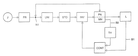
Represented in figure 1 is a block diagram for a
circuit arrangement according to the invention for
starting and operating discharge lamps. At connection
terminals J, a line voltage from a line voltage source
can be fed to the circuit arrangement. The line
voltage is initially fed into a block FR. On the one
hand, this block includes known means for filtering
CA 02456371 2004-O1-27
_ g _
disturbances. On the other hand, this block includes a
rectifier, which rectifiers the line voltage, which is
an AC voltage. Usually, a bridge-connected full-wave
rectifier is used for this purpose. Important for the
function of a charge pump realized in the circuit
arrangement is the property of the rectifier that it
does not permit any current that allows an energy flow
from the circuit arrangement to the line voltage
source.
The rectified line voltage is fed to an electronic
pumping switch UNI, a pumping node N1 being produced at
the connecting point between the rectifier FR and the
electronic pumping switch UNI. In the simplest case,
the electronic pumping switch UNI comprises a pumping
diode, which only allows a current flow that flows from
the pumping node N1 to the pumping diode. It is also
possible, however, to use any desired electronic
switch, such as for example a MOSFET, for the
electronic pumping switch UNI that performs the
function of the pumping diode.
The current which the electronic pumping switch UNI
allows through feeds a main energy store STO. The main
energy store STO is usually configured as an
electrolytic capacitor. However, other types of
capacitors are also possible. In principle, the dual
form of energy storage with respect to the capacitor is
also possible. In the dual case, the main energy store
STO is configured as a coil. Because of the lower
costs and the better efficiency, a capacitor is
preferred as the main energy store STO.
There are also configurations of charge pumps with a
number of so-called pumping branches. In this case, a
number of electronic pumping switches UNT are connected
in parallel. This produces a number of pumping nodes
Nl. For the mutual decoupling of the pumping nodes, a
diode is connected in each case between the rectifier
CA 02456371 2004-O1-27
_ g
and the pumping node. An exemplary embodiment with two
pumping branches is represented in figure 2.
The main energy store STO provides its energy to an
inverter INV. The inverter INV generates an
alternating variable, usually an AC voltage, which is
fed to a block, which is designated by MN and PN. MN
designates the function of the block as a match ing
network. With respect to this function, the bl ock
MN/PN can be connected to a discharge lamp L. PN
designates the function of the block as a pump ing
network. With respect to this function, the bl ock
MN/PN is connected to the pumping node Nl. The
connecting line between the pumping node N1 and the
block MN/PN is provided in figure 1 with an arrow at
both ends. This is intended to indicate that ene rgy
flows in an alternating manner from the pumping node N1
to the block MN/PN and back. The functions of the
matching network and of the pumping network are
combined in the block MN/PN because embodiments of the
invention in which individual components can be
assigned both to one and the other function are
possible.
A controller CONT, which uses a manipulated variable to
act on the inverter INV, is provided for controlling a
desired first. operating variable. Consequently, a
parameter of the alternating variable delivered by the
inverter, for example the operating frequency or the
pulse width, is changed in such a way that changing of
the first operating variable is counteracted. The
first operating variable is fed to a first input of the
controller via the terminal B1. The first operating
variable is a variable which determines the operation
of the lamp. Therefore, in figure 1 the terminal Bl
originates from the block for the discharge lamp L.
The first operating variable is, for example, the lamp
current or the lamp power. These variables to not have
CA 02456371 2004-O1-27
- 10 -
to be recorded directly on the discharge lamp L, but
can also be taken from the block MN/PN.
According to the invention, the controller CONT has a
second input. A second operating variable is fed to
the second input via a threshold switch TH. According
to the invention, the second operating variable is a
measure of the reactive energy that resonates in a
resonant circuit contained in the block MN/PN. The
tapping of the second operating variable by means of
the terminal B2 therefore takes place at the block
MN/PN. It is also possible, however, to obtain a
measure of said reactive energy from lamp operating
variables, such as for example the lamp voltage.
For igniting the discharge lamp L, reactive energy is
built up in the resonant circuit. The reactive energy
provides information on the energy imbalance of the
charge pump and the loading of components. If the
second operating variable exceeds the threshold of the
threshold switch, according to the invention the
rectifier is influenced by the controller CONT in such
a way that the reactive energy does not increase any
further. This can take place by the operating
frequency of the inverter INV being raised. The
controller CONT may include an adder, which adds the
signals present at the controller inputs. It must be
ensured that the signal at the first controller input
does not clamp the signal at the second controller
input. If the signal at the second controller input
exceeds the signal at the first controller input, the
signal at the second controller input must be the
decisive controller signal.
Represented in figure 2 is an exemplary embodiment of a
circuit arrangement according to the invention for
starting and operating discharge lamps.
CA 02456371 2004-O1-27
- I1 -
A line voltage can be connected to the terminals J1 and
J2. The line voltage is fed via a filter, comprising
two capacitors C1, C2 and twa coils L1, L2, to a full-
bridge rectifier comprising the diodes D1, D2, D3, D4.
The full-bridge rectifier provides the rectified line
voltage at its positive output, a node N21, with
respect to a reference node N0.
The rectified line voltage is fed via the diodes D5 and
D6 to two pumping nodes N22 and N23. The exemplary
embodiment in figure 2 accordingly has two pumping
branches. The diodes D5 and D6 are necessary for
decoupling the pumping branches from each other. When
there is only one pumping branch, a pumping node can be
connected directly to the rectifier output, the node
N21. In this case, however, it must be ensured that
the diodes used in the rectifier can switch quickly
enough to follow the inverter frequency. If this is
not the case, a high-speed diode must be connected
between the rectifier output and the pumping nodes even
when there is only one pumping branch. In the
exemplary embodiment in figure 2, the pumping nodes are
coupled to the positive output of the rectifier.
Charge pump topologies in which pumping nodes are
coupled to the negative output of the rectifier are
also known from the literature.
Leading from the pumping nodes N22 and N23 to the node
N24 there is respectively an electronic pumping switch,
configured as diodes D7 and D8. Connected between N24
and NO is the main energy store, which is configured as
electrolytic capacitor C3.
C3 feeds the inverter, which is configured as a half
bridge. Other converter topologies, such as for
example a flyback converter or full bridge, can also be
used, however. A half bridge is advantageously used
for lamp powers of between 5 W and 300 W, since it
represents the lowest-cost topology.
CA 02456371 2004-O1-27
- 12 -
The half bridge essentially comprises a series
connection of two half-bridge transistors T1 and T2 and
a series connection of two coupling capacitors C4 and
C5. Both series connections are connected in parallel
with C3. A connecting node N25 of the half-bridge
transistors and a connecting node N26 of the coupling
capacitors form the inverter output at which a square-
wave inverter voltage with an inverter frequency is
present.
Connected between N25 and a lamp voltage node N27 is a
lamp inductor L3. Connected at N27 is the terminal J3,
at which the series connection of two discharge lamps
Lpl and Lp2 is connected in the exemplary embodiment.
However, the present invention can also be configured
with one or more lamps. The current through the
discharge lamps Lp1 and Lp2 flows via a terminal J8,
through a winding W1 of a measuring transformer to the
node N26. Consequently, the inverter voltage is
essentially applied to a series connection of two
discharge lamps Lpl, Lp2 and the lamp inductor L3.
The current fed into J3 flows not only through the gas
discharge of the discharge lamps Lpl, Lp2 but also
through an outer filament of the first discharge lamp
Lp1 to a terminal J4. From there, it continues through
a winding W4 of a heating transformer, on through a
variable resistor Rl and on through a winding W3 of the
measuring transformer to the terminal J7. Connected to
the terminal J7 is an outer filament of the second
discharge lamp Lp2, the other end of which leads to the
terminal J8. Two inner filaments of the discharge
lamps Lpl and Lp2 are respectively connected via the
terminals J5 arid J6 to the winding W5 of the heating
transformer. By the arrangement described in this
paragraph, the inverter voltage brings about not only a
current through the gas discharge of the discharge
lamps Lpl, Lp2 but also a heating current through the
CA 02456371 2004-O1-27
_ 13 _
outer filaments and, via the heating transformer, also
a heating current through the inner filaments of the
discharge lamps Lpl, Lp2. If only one discharge lamp
is to be operated, it is possible to dispense with the
heating transformer.
The heating current is essentially required before the
ignition of the discharge lamps Lpl, Lp2, during a
preheating phase as a preheating current for the
preheating of the filaments. The value of the heating
current is determined largely by the variable resistor
R1. During the preheating phase, the value of R1 is so
low that a heating current prescribed by lamp data is
achieved. After the preheating phase, the value of R1
increases, so that negligible heating current flows in
comparison with the current through the gas discharge
of the discharge lamps Lpl, Lp2. In the exemplary
embodiment, Rl is realized by a so-called PTC or
positive temperature coefficient thermi.stor. This is a
resistor which in the cold state has a low resistance.
The PTC thermistor is heated up by the heating current,
making its resistance value increase. R1 may also be
realized by an electronic switch which is closed in the
preheating phase and then open. A resistor with a
constant resistance value may be connected in series
with the switch. Consequently, a rapid transition from
the preheating phase to the igniting phase is possible.
The described arrangement for preheating the filaments
has the effect that, during the preheating phase, the
resonant frequency of a resonant circuit described in
the next paragraph is lower than its natural frequency,
due to damping. An inverter frequency which lies below
the natural frequency is advantageously chosen during
the preheating phase, in order to obtain a high heating
current, and consequently a short preheating phase.
The lamp voltage node N27 is connected to the pumping
node N23 via a first resonant capacitor C6. Connected
CA 02456371 2004-O1-27
- 14 -
between N23 and NO is a second resonant capacitor C7.
C6 and C7 form with the lamp inductor L3 a resonant
circuit. For fixing the natural frequency of the
resonant circuit, C6 and C7 are viewed as connected in
series. The effective capacitance value of C6 and C7
with respect to the natural frequency is consequently
the quotient of the product and the sum of the
capacitance values of C6 and C7. If the resonant
circuit is stimulated close to its natural frequency,
an ignition voltage that leads to the ignition of the
discharge lamps is produced across the lamas. After
the ignition, L3 acts together with C6 and C7 as a
matching network, which transforms an output impedance
of tha inverter into an impedance necessary for the
operation of the discharge lamps.
The connection of C6 and C7 to the pumping node N23 has
the effect, however, that the combination of L3, C6 and
C7 acts not only as a resonant circuit and matching
network but at the same time as a pumping network. If
the potential at N23 is lower than the momentary line
voltage, the pumping network L3, C6, C7 draws energy
from the line voltage. If the potential at N23 exceeds
the voltage at the main energy store C3, the energy
accepted from the line voltage is delivered at C3. The
choice of the ratio of the capacitance values of C6 and
C7 allows the effect of the network L3, C6, C7 as a
pumping network to be adjusted. The greater the
capacitance value of C7 is chosen to be, the less the
network L3, C6, C7 acts as a pumping network.
A further pumping effect is produced by a capacitor C8,
which is connected between N23 and the connecting node
N25 of the half-bridge transistors T1, T2. C8 also not
only acts as a pumping network but at the same time
performs the task of a snubber capacitor. Snubber
capacitors are generally known as a measure for switch
relief in inverters.
CA 02456371 2004-O1-27
- 15 -
The pumping network for the second pumping branch
comprises the series connection of a pumping inductor
L4 and a pumping capacitor C9. This pumping network is
connected between the connecting node N25 of the half-
bridge transistors T1, T2 and the pumping node N22. In
the case of the present exemplary embodiment, two
pumping branches are used, in order that the pumped
energy is divided between a number of components.
Lower-cost dimensioning of the components is
consequently possible. It also provides a degree of
freedom in the design of the dependence of the pumped
energy on operating parameters of the discharge lamps.
However, the invention can also be realized with only
one pumping branch.
The half-bridge transistors Tl, T2 are designed as
MOSFETs. Other electronic switches may also be used
for this. For activating the gates of Tl and T2, an
integrated circuit ICl is provided in the exemplary
embodiment. IC1 is in the present example a circuit of
the type IR2153 from the company International
Rectifier. Alternative circuits of this type are also
available on' the market; for example L657i from the
company STM. The circuit IR2153 includes a so-called
high-side driver, with which the half-bridge transistor
T1 can also be activated, although it has no connection
at the reference potential N0. A diode D10 and a
capacitor C10 are necessary for this purpose.
The operating voltage supply of the IC1 takes place via
the terminal 1 of the IC1. In figure 2, a voltage
source VCC is provided for this purpose between
terminal 1 of the ICl and N0. Several possible ways in
which this voltage source VCC can be realized are
generally known. In the simplest case, the IC can be
supplied via a resistor from the rectified line
voltage.
CA 02456371 2004-O1-27
- 16 -
Apart from the driver circuits for the half-bridge
transistors, IC1 includes an oscillator, the
oscillating frequency of which can be set via the
terminals 2 and 3. The oscillating frequency of the
oscillator corresponds to the inverter frequency.
Connected between the terminals 2 and 3 is a frequency-
determining resistor R3. Connected between terminal 3
and NO is the series connection of a frequency-
determining capacitor C11 and the emitter-collector
path of a bipolar transistor T3. Connected in parallel
with the emitter-collector path of T3 is a diode D9, in
order that C11 ca.n be charged and discharged. The
inverter frequency can be set by a voltage between the
base terminal of T3 and NO and consequently forms a
manipulated variable for the control circuit. The base
terminal of T3 is connected to a manipulated-variable
node N28. T3, IC1 and their wiring can consequently be
regarded as a controller.
The functions of the IC1 and its wiring can also be
realized by any desired voltage-controlled or current-
control oscillator which brings about the activation of
the half-bridge transistors via driver circuits.
The control circuit in the exemplary embodiment records
as a controlled variable the current through the gas
discharge of the discharge lamps Lpl, Lp2. For this
purpose, the measuring transformer has a winding W2.
The winding direction in the measuring transformer is
designed such that the heating current in the winding
W3 is subtracted from an overall current in winding W1,
so that in winding W2 there flows a current which is
proportional to the current through the gas discharge
of the discharge lamps Lpl, Lp2. A full-bridge
rectifier, formed by diodes D11, D12, D13 and D14,
rectifies the current through winding W2 and leads it
via a low-resistance measuring resistor R4 to N0. The
voltage drop across R4 is consequently a measure of the
current through the gas discharge of the discharge
CA 02456371 2004-O1-27
- 17 -
lamps Lpl, Lp2. Passing via a low-pass filter for
averaging, which is formed by a resistor R5 and a
capacitor C13, the voltage drop across R4 reaches the
input of a noninverting measuring amplifier.
The measuring amplifier is realized in a known way by
an operational amplifier AMP and the resistors R6, R7
and R8. In the exemplary embodiment, a gain of the
measuring amplifier of about 10 is set. In the event
that the voltage drop across R4 has values which can be
used directly as a manipulated variable, it is possible
to dispense with the measuring amplifier or replace it
with an impedance converter, such as for example an
emitter follower.
The output of the measuring amplifier is connected via
a diode D15 to the manipulated-variable node N28.
Consequently, the control circuit for controlling the
current through the gas discharge of the discharge
lamps Lpl, Lp2 is closed. The diode D15 is necessary
in order that the potential of N28 can be raised to a
value that h'ies above the value prescribed by the
measuring amplifier. The anode of D15 represents a
first controller input.
The threshold switch according to the invention is
realized in figure 2 by a varistor MOV. It lies in a
series connection with a capacitor C12, a resistor R2
and a diode D17, which connects the voltage node N27 to
the manipulated-variable node N28. The anode of D17
represents a second controller input. N28 is connected
via the parallel connection of a resistor R9 and a
capacitor C14 to N0.
At N27 there is with respect to NO a voltage which is a
measure of the reactive energy resonating in the
resonant circuit, formed by L3, C6 and C7. If this
voltage exceeds the threshold voltage of the varistor
MOV, a current flows through R9, and C14 is charged.
CA 02456371 2004-O1-27
- 18 -
The voltage at the manipulated-variable node N28 is
consequently raised. This brings about an increase in
the inverter frequency, and the reactive energy
resonating in the resonant circuit is reduced, since
the inverter frequency shifts further away from the
natural frequency of the resonant circuit.
Connected between NO and the connecting point of R2 and
D17 is the diode D16. Consequently, acting together
with C12, the sum of the positive amplitude and
negative amplitude of the voltage which the varistor
MOV allows to pass is applied to N28. Instead of the
varistor MOV, any other desired threshold switch may be
used, such as can be constructed for example by 2ener
diodes or suppressor diodes. The threshold value of
the varistor MOV is chosen in the application example
as 250 Vrms. A higher value has the effect that more
reactive energy is allowed in the resonant circuit,
which leads to a higher ignition voltage at the
discharge lamps Lpl, Lp2, but also leads to a greater
loading of components. Consequently, a desired optimum
can be set by means of the threshold value of the
varistor MOV..
The value of the resistor R2 influences the intensity
of the effect of the intervention according to the
invention on the control circuit at the manipulated-
variable node N28. A nonlinear relationship between
the voltage at the manipulated-variable node N28 and
the inverter frequency is also advantageous. This
nonlinear relationship is realized in the application
example by the nonlinear characteristic of T3.
Moreover, it is influenced by the dependence of the
frequency of the oscillator in the IC1 on the voltage
at the terminal 3 of the IC1. Due to the nonlinearity,
a strong increase in the voltage at N27 leads to a
disproportionate increase in the inverter frequency,
whereby overloading of components, such as for example
CA 02456371 2004-O1-27
- 19 -
the voltage loading of C3 or the current loading of TI
and T2, is prevented.
Instead of the voltage, the current in the resonant
circuit could also be used as a measure of the reactive
energy resonating in the resonant circuit. An
additional winding on L3 could serve this purpose, for
example.