Note: Descriptions are shown in the official language in which they were submitted.
CA 02456379 2009-02-06
PRINTED CIRCUIT BOARD DIPOLE ANTENNA STRUCTURE
WITH IMPEDANCE MATCHING TRACE
Cross-Reference to Related Applications
Field of the Invention
[0002] The present invention generally relates to the field of antennas for
transmitting
radio frequency signals. More particularly, the present invention relates to a
printed antenna
comprised of thin layers of electrically conductive material that are bonded
onto a thin, planar
dielectric material such as a printed circuit board (PCB) that also serves as
a platform for an
antenna driving circuit.
Background of the Invention
[0003] Presently, the desire for antennas for transmitting radio frequency
signals from a
small, compact location to an external receiver has grown significantly. For
example, antennas
for transmitting radio frequency signals from a recording or monitoring
device, such as a
thermostat, water meter, gas meter, electric meter or any similar type of
device to a remote
location that is configured to monitor and record the status of the device
have become
increasingly desirable. Since many of the devices utilizing an RF antenna are
produced in very
large quantities, a desire and need exists for an antenna that can transmit
the RF signals a desired
distance while being low in cost to produce and assemble.
[0004] Typically, an antenna structure is formed separate from the printed
circuit board
that includes the antenna driving circuit. The separate antenna device
increases the cost to
produce the combination of the antenna and driving circuit while also
increasing the size of the
compartment needed to house the two separate components.
[0005] In an effort to avoid the use of external antennas, manufacturers have
utilized
micro strip patch antennas, the characteristics of which are well known.
Briefly, a micro strip
patch antenna includes a dielectric material, such as a printed circuit board,
which has two
opposed surfaces. One of the surfaces is coated with an electrically
conductive layer that
functions as a ground plane and the opposed surface
CA 02456379 2004-01-28
has an essentially rectangular or circular shaped electrically conductive
layer (micro
strip patch) disposed to extend over the ground plane. The micro strip patch
antenna
presents a thin resonating cavity where standing electromagnetic waves can
exist and
can be radiated from the edges of the antenna.
[0006] Micro strip patch antennas, however, have many limitations, including
the ability to radiate only above the ground plane. Further, because the micro
strip
patch antenna has a resonant cavity that greatly depends upon the thickness of
the
dielectric material utilized, tuning such an antenna is difficult. Thus, the
printed
circuit board forms a important part of the antenna structure, even though a
PCB is
typically formulated with rather low tolerances.
[0007] Therefore, it is an object of the present invention to provide a
printed
antenna that can be formed directly on a dielectric material, such as a
printed circuit
board, that also is used to mount the antenna driving circuitry. Further, the
present
invention seeks to provide a printed circuit antenna that functions as a
dipole antenna
having a radiating portion significantly less than one-half the wave length of
the
received/transmitted frequency range. The antenna also provides an impedance
matching strip that allow the antenna to match the impedance of the antenna
driving
circuit by increasing or decreasing the length and configuration of the
impedance
matching strip.
Summary of the Invention
[0008] The present invention is a printed antenna for the transmission of
electromagnetic waves, such as radio frequency signals, from. an electrical
device
coupled to the printed antenna. The printed antenna of the present invention
is
designed for use in communicating information from a measurement device, such
as
an electronic thermostat, gas meter, water meter, electric meter or similar
device.
However, the printed antenna of the present invention can be utilized for
transmitting
information from any device that incorporates an antenna. driving circuit
mounted to a
printed circuit board.
[0009] The printed antenna of the present invention includes a substantially
planar printed circuit board that is formed from a dielectric material. The
printed
circuit board is a conventional component and is utilized to mount an antenna
driving
2
CA 02456379 2004-01-28
circuit that operates to generate electromagnetic waves for transmission and
receives
electromagnetic information from a remote transmission device. The circuit
board
includes a planar first surface and a planar second surface that are separated
by a
material thickness.
[0010] The circuit board is a unitary structure and is configured to include
both
a mounting section and an antenna section. The mounting section of the circuit
board
includes the antenna driving circuit for the printed antenna. Specifically,
the antenna
driving circuit is mounted to the first surface of the circuit board within
the mounting
section.
[0011] The second planar surface of the mounting section of the circuit board
includes a coating of electrically conductive material that covers
substantially all of
the mounting section. Thus, the coating of electrically conductive material
that
defines the ground plane is positioned on the opposite side of the circuit
board from
the antenna driving circuit such that the antenna driving circuit is
positioned opposite
the area defined by the ground plane.
[0012] The antenna section of the circuit board includes both a first antenna
trace and a second antenna trace that form opposite halves of a one-half
wavelength
dipole antenna. Each of the antenna traces is formed frorn an electrically
conductive
material printed onto the face surface of the circuit board.
[0013] Each antenna trace includes a connecting strip that couples the antenna
trace to either ground or the active connection of the antenna driving
circuit. Since the
antenna traces are a mirror images of the opposite antenna trace, the
configuration of
each antenna trace is identical.
[0014] Each antenna trace includes a radiating strip extending from the
connection strip. The combined length of the two radiating strips is less than
one-half
the wavelength of the desired frequency that the antenna structure radiates
and
receives.
[0015] As such, each antenna trace also includes an impedance matching strip
coupled to the radiating strip. The impedance matching strip is a serpentine
structure
and is coupled to the radiating strip by a connecting trace. The connecting
trace forms
a connection between the radiating strip and the impedance matching strip and
is
3
CA 02456379 2004-01-28
configured depending upon the overall shape of the printed circuit board. The
impedance matching strip is joined to the radiating strip to define a
continuous length
of electrically conductive mat:erial applied to the front face surface of the
antenna
section. The impedance matching strip is coupled to the radiating strip and
has a
length such that the impedance matching strip functions to match the impedance
of the
antenna driving circuit.
[0016] In the preferred embodiment of the invention, the impedance matching
strip includes a plurality of parallel legs joined to each other and coupled
to the
radiating strip. Each leg of the impedance matching strip is parallel to the
radiating
strip. The legs of the impedance matching strip are joined to each other by
connector
portions such that the entire impedance matching strip is a continuous trace
applied to
the face surface of the antenna section.
[0017] In a preferred embodiment of the invention, one of the legs of the
impedance matching strip is shorter than the remaining legs such that the leg
acts as a
tuning stub. The length and characteristics of the tuning stub can be adjusted
to fine
tune the impedance matching strip to the impedance requirement of the antenna
driving circuit.
[0018] Various other features, objects and advantages of the invention will be
made apparent from the following description taken together with the drawings.
Brief Description of the Drawings
[0019] The drawings illustrate the best mode presently contemplated of
carrying
out the invention.
[0020] In the drawings:
[0021] Fig. 1 is a front plan view of a printed circuit board including the
printed
dipole antenna of the present invention;
[0022] Fig. 2 is a detailed illustration of the printedl dipole antenna
including an
impedance matching strip;
[0023] Fig. 3 is a section view taken along line 3-3 of Fig. 1;
[0024] Fig. 4 is a perspective illustration showing the axes of rotation of
the
printed circuit board dipole antenna structure during radiation testing;
4
------------- - ------
CA 02456379 2004-01-28
[0025] Fig. 5 is a 3-D radiation pattern for the printed circuit board dipole
antenna structure of the present invention;
[0026] Fig. 6 is a graphic illustration of the radiation pattern of the
antenna of
the present invention as rotated along the Z axis; and
[0027] Fig. 7 is a graph illustration illustrating the SWR over a frequency
range
of 900 MHz to 960 MHz.
Detailed Description of Preferred Embodiments
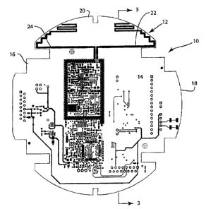
[00281 Referring first to Fig. 1, thereshown is a pr:inted circuit board 10
including both a printed circuit board dipole antenna structure 12 and an
antenna
driving circuit 14. The antenna driving circuit 14 includes various electronic
components for driving and receiving signals from the printed dipole antenna
structure
12 of the present invention. The antenna driving circuit 14 both applies and
receives
radio frequency energy from the printed dipole antenna 12. The antenna driving
circuit 14 is mounted to the first, front surface of the circuit board 16 in a
known
manner, such as by automated surface mount technology techniques. The antenna
driving circuit 14 is a conventional configuration and is well known to those
skilled in
the art. Many different configurations for the antenna driving circuit 14 are
contemplated as being within the scope of the present invention. The specific
configuration of the antenna driving circuit 14 is not shown, since the
specific
configuration of the antenna driving circuit 14 does not form part of the
present
invention.
[0029] As can be seen in Fig. 1, the circuit board 16 has a generally circular
configuration, since the circuit board 16 shown in the preferred embodiment of
the
invention is for use within an electric meter. However, it should be
understood that
the physical configuration of the circuit board 16 depends upon its operating
environment and thus can vary depending upon the specific application.
[0030] As illustrated in Fig. 1, the printed circuit board 10 includes both a
component mounting section 18 and an antenna section 20. The component
mounting
section 18 and the antenna section 20 are integrally formed with each other
and form
the unitary printed circuit board 10. In the preferred embodiment of the
invention
shown in Fig. 3, a layer of conductive coating 21 is applied to the second,
back face
CA 02456379 2004-01-28
surface of the component mounting section 18 to provide a ground plane for the
antenna driving circuit 14 mounted to the front face surface of the circuit
board within
the component mounting section 18. Preferably, the coating of electrically
conductive
material is an applied copper coating that defines the ground plane for the
printed
circuit board 10. Although copper is used in the present invention, other
conductive
coatings, such as gold, silver, etc., are contemplated as being within the
scope of the
present invention.
[0031] The ground plane formed by the layer of electrically conductive
material
21 is positioned beneath only the component mounting section 18 and is not
applied to
the back surface of the printed circuit board beneath the antenna section 20.
[0032] As illustrated in Fig. 1, the antenna section 20 includes a first
antenna
trace 22 and a second antenna trace 24. The first and second antenna traces
22, 24
function as both sides of a one-half wavelength dipole antenna for
transmitting
electromagnetic waves generated by the antenna driving circuit 14 and for
receiving
electromagnetic waves and transferring the received signals to the antenna
driving
circuit 14.
[0033] In the preferred embodiment of the invention, the dipole antenna
structure 12 is configured to transmit signals in the range of 900 MHz-960
MHz. As
such, the antenna 12 is driven by a circuit that requires an impedance of
approximately
50 ohms. Therefore, an impedance matching circuit that offsets the antenna
impedance as close to 50 ohms is desired. The proper impedance matching
facilitates
proper operation of the system, in both the receive and transmit modes.
[0034] Referring now to Fig. 2, thereshown are the details of the first
antenna
trace 22 and the second antenna trace 24. In the following description, the
dimensions
for the various components of the antenna traces 22 and 24 are set forth.
However, it
should be understood that the actual dimensions for the traces 22 and 24 will
vary
depending on the size of the circuit board and the transmission and receiving
frequency of the antenna. As illustrated, the first and second antenna traces
22, 24 are
mirror images of each other such that both sides of the dipole antenna are
matched.
The first antenna trace 22 includes a connection strip 26 that connects the
first antenna
trace 22 to the ground plane for the antenna driving circuit. The second
antenna trace
6
CA 02456379 2004-01-28
24 includes a similar connecting strip 28 that couples the second antenna
trace 24 to
the active driving components of the antenna driving circuit 14. Both the
first and
second connecting strips 26, 28 are parallel to each other, as illustrated.
[0035] Each of the connecting strips 26, 28 are electrically coupled to a
radiating strip 30. As illustrated in Fig. 2, the radiating strips 30 extend
in opposite
directions and each have a length of 1.564 inches, such that the combination
of the two
radiating strips 30 has a combined length of 3.128 inches. Since the antenna
structure
of the present invention functions as a one-half wavelength dipole antenna,
the
required length of the antenna is approximately 6.5 inches for the optimal
radiation of
signals having a center frequency of 930 MHz. Since the circuit board 16 shown
in
Fig. 1 must fit within the housing of a conventional electric meter, the
length of the
radiating strips 30 are limited by the physical configuration of the antenna
enclosure.
[0036] To compensate for the reduced length of the radiating strips 30, each
of
the first and second antenna traces 22, 24 includes an impedance matching
strip 32.
The impedance matching strip of the first antenna trace 22 and the second
antenna
trace 24 are identical to each other such that each side of the dipole antenna
structure
is matched to the opposite side of the antenna structure.
[0037] As shown in Fig. 2, the impedance matching strip 32 is electrically
coupled to the radiating strip 30 by a connecting trace 34. In the embodiment
of the
invention illustrated in Figs. 1 and 2, the connecting trace 34 has a stair-
like pattern.
This stair-like pattern is dictated by the physical configuration of the
circuit board 16
onto which it is printed and forms no part of the present invention. The
connecting
trace 34 is a simple electrical connection between the radiating strip 30 and
the
impedance matching strip 32. It is contemplated by the inventors that the
physical
configuration of the connection trace 34 could be varied or even eliminated
depending
upon the physical configuration of the circuit board 16 and the space
availability on
the antenna section 20.
[0038) Referring back to Fig. 2, the impedance matching strip 32 in the
preferred embodiment of the invention has a generally seipentine configuration
and
has an overall length selected to match the approximately 50 ohm impedance of
the
antenna driving circuit 14, as previously discussed. The impedance matching
strip 32
7
CA 02456379 2004-01-28
includes a first leg 36 that is parallel to the radiating strip 30 and spaced
from the
radiating strip 30. In the preferred embodiment of the invention illustrated
in Fig. 2,
the first leg 36 has a length of 0.7 inches and is spaced from the radiating
strip by
0.411 inches.
[0039] The impedance matching strip 32 further includes a second leg 38 joined
to the first leg 36 by a connecting section 40. The second leg 38 is parallel
to the first
leg 36 and has a length less than the length of the first leg 36. In the
preferred
embodiment of the invention illustrated in Fig. 2, the second leg 38 has a
length of
approximately 0.505 inches.
[0040] The second leg 38 is joined to a third leg 42 by a second connecting
portion 44. The third leg 42 has the same overall length as the second leg 38.
As
illustrated in Fig. 2, the first leg 36, the second leg 38 and the third leg
42 are all
parallel to each other and parallel to the radiating strip 30. The combination
of the
parallel legs and connection sections function as an impedance matching
circuit for the
antenna driving circuit.
[0041] The impedance matching strip 32 further includes a tuning stub 46
connected to the third leg 42 by a connecting portion 48. The tuning stub 46
has a
length of 0.367 inches, which is less than the length of the third leg 42. The
length of
the tuning stub 46 can be modified to fine tune the impedance matching
characteristics
of the impedance matching strip 32 to the specific antenna driving circuit to
provide a
more accurate and specific impedance matching. The length of the tuning stub
46 can
be easily and readily modified during construction of the printed circuit
antenna 10
without requiring a redesign of the entire impedance matching strip 32.
[0042] In the preferred embodiment of the invention, the first antenna trace
22
and the second antenna trace 24, which include the pair of connecting strips
26, 28, the
pair of radiating strips 30 and the pair of impedance matching strips 32 are
all
comprised of a layer of electrically conductive material, such as copper,
disposed on
the front face surface 49 of the circuit board 16, as shown in Figo 3.
Specifically, the
traces are applied to the antenna section 20 of the circuit board. The copper
material
used to form the pair of antenna traces 22 and 24 include a protective outer
coating, as
is conventional.
8
CA 02456379 2004-01-28
[00431 Referring now to Fig. 4, thereshown is the dipole antenna structure 12
as
positioned along an X-Y-Z coordinate system. The X-Y-Z coordinate system shown
in Fig. 3 will be used as a reference for the radiating results to be
described as follows.
[0044] Referring first to Fig. 5, thereshown is the radiation pattern of the
antenna of the present invention along the X, Y and Z axes. As illustrated in
Fig. 5,
the printed circuit board antenna 10 of the present invention exhibits a
uniform
radiation pattern both above and below the antenna.
[0045] Fig. 6 illustrates the radiation pattern when the antenna 12 is rotated
360 about the Z axis when oriented as illustrated in Fig. 4.
[0046) Fig. 7 illustrates the predicted standing wave ratio (SWR) for a
frequency range between 900 MHz and 960 MHz. As illiastrated, the SWR drops
from
approximately 3.8 at 900 MHz to a low value around 930 MHz and again increases
to
a value of approximately 4 as the frequency rises to 960 MHz. The antenna of
the
present invention is intended to be used from approximately 900 MHz to
approximately 960 MHz.
[0047] While the preferred embodiment of the printed antenna of the present
invention has been described with certain particularly for the purposes of
illustration,
it should be noted that various modifications may be made while keeping within
the
spirit of the present invention. For example, while the specific length and
configuration of the impedance matching strips 32 are shown in the Figures, it
should
be understood that the impedance matching strip could be configured in
different
manners to provide the required impedance matching for the antenna driving
circuit.
Additionally, although specific dimensions and shapes are shown for the
circuit board,
it should be understood that different circuit board sizes and shapes could be
utilized.
When such different sized circuit boards are utilized, the configuration of
the
impedance matching strip, and the connecting strip, would vary. Additionally,
although the present invention is described as being particularly desirable in
transmitting RF signals from commodity measuring devices, such as an electric
meter,
gas meter, or water meter, it should be understood that the printed circuit
board
antenna of the present invention could be utilized in many other operating
environments while operating within the scope of the present invention.
9
CA 02456379 2004-01-28
[0048] Various alternatives and embodiments are contemplated as being within
the scope of the following claims particularly pointing out and distinctly
claiming the
subject matter regarded as the invention.