Note: Descriptions are shown in the official language in which they were submitted.
CA 02456671 2004-02-06
SPECIFICATION
LIGHT EMITTING OR LIGHT RECEIVING SEMICONDUCTOR MODULE
AND MAhING METHOD THEREOF
TECHNICAL FIELD
The present invention relates to a light emitting or light receiving
module including a plurality of substantially spherical semiconductor devices,
and to a making method thereof. This light emitting or light receiving
semiconductor module can be applied to a variety of applications such as a
solar cell panel, a lighting panel, a display, and a semiconductor
photocatalyst.
BACKG ROUND ART
Conventionally, research has been directed toward a technology that
involves forming a pn junction. via a diffusion layer, on a surface of a
small-diameter spherical semiconductor element made of a p-type or n-type
semiconductor and then conriecting a plurality of these spherical
semiconductor elements in parallel to a common electrode, this technology
being put to practical use for solar cells, semiconductor photocatalysts, and
so
forth.
U.S. Patent No. 3,998,659 discloses an example in which a solar cell is
constituted by forining a p-tvpe diffu9ion layer on the surface of a n-type
spherical semiconductor, connecting the respective diffusion layers of a
plurality of spherical semiconductors to a common film-like electrode
1
CA 02456671 2004-02-06
(positive electrode), and then connecting the n-type core sections of these
spherical semiconductors to a common film-like electrode (negative
electrode).
U.S. Patent No. 4,021.323 discloses a solar energy converter
(semiconductor module) having the following constitution, Plural p-type
spherical semiconductor elements and plural n-type spherical semiconductor
elements are placed in series, and connected to a common film-hke electrode,
and respective diffusion layers of these semiconductor elements are made
into contact with a common electrolytic solution, and then by irradiating with
solar light, electrolysis of the electrolytic solution is induced.
So too in the case of the modules having spherical cells appearing in
U.S. Patent Nos. 4,582,588 and 5,469,020, because the spherical cells are
attached by being connected to a sheet-like common electrode, a plurality of
spherical cells are suitable for connecting in parallel. However, they are not
suitable for serial connection.
On the other hand, as shown in International Patent Publication Nos.
W098/15983 and 'VV099/10935, the invent.or of the present invention has
proposed a granular light emitting or light receiving semiconductor device in
which a diffusion layer, pn junct.ion, and a pair of electrodes are formed on
a
spherical semiconductor element made of a p-type semiconductor or an
n-type semicoi-iduct.or. .Also, proposed is a semiconduetor module, which is
produced by connecting a plurality of the semiconductor device in series and
then connecting a plurality of the serially connected bodies in parallel, and
which can be applied to a solar cell, a photocatalyst device for electrolysis
of
2
CA 02456671 2004-02-06
water and so forth, a variety of light emitting devices, and color displays,
and
the like.
In the case of this semiconductor module, when anv semiconductor
device of any serially connected body enters an open state due to failure,
current no longer flows to the serial circuit including above failed
semiconductor element, and the remaining normal semiconductor devices in
the serially connected body also enter a breakdown state, whereby dropping
of the output of the semiconductor module is generated.
In addition, in the case of the spherical semiconductor devices having
the positive and negative electrodes that were proposed by the present
inventor, handling is a problem because the device is prone to rolling, and it
is not easy to determine the position for forming the positive and negative
electrodes nor to distinguish the positive and negative electrodes during
assembly.
Therefore, the inventor of this application undertook research with
respect. to a technology for forming a pair of flat surfaces on a spherical
semiconductor elenient and then for forming electrodes on these flat surfaces.
However, not only was there then a large number of processes for the
electrode foxmation, it also became evident that it was still not easy to
distinguish between the positive and negative electrodes and that this
technology was not very advaiitageous in terms of mass producing the
semiconductor module by using a multipl-lcity of sphei-ical semiconductor
devices.
An object of the present invention is to provide a light emitting or
3
CA 02456671 2008-11-28
light receiving semiconductor module that makes it possible to keep any
decrease in the
output voltage and current to a ni{nimum even when any seniiconductor devioe
fails, as well
as a ndalCing method thereof. Another objeot of the present invention is to
provide a light
emitting or light receiving semiconductor module that facilitates distinction
between the pair
of electrodes of the granular semiconductor device, as well as a making method
thereo The
other object of the present invention is to provide a light emitting or light
receiving
semiconductor module that also makes it possible to guide light to a position
at an interval
from the point ofiitoidence or light emission point via the reflective action
of an optical
transmission member, as well as a making method thereof.
DISCLOSURE OF THE INVENTION
A light emitting or light receiving semiconductor module according to one
aspect of
the present invention comprises: a plurality of substantially spherical
semiconductor devices
with a light emitting or light receiving fanction arranged in a plurality of
rows and a plurality
of columns with an aligned conduction direction; and a conductive connection
mechanism,
which electrically conneots the plurality of semioonductor devices of each
column in series
such that for each individual column the semiconductor devices therein are
serially connected
with each other and said conductive connection meGhanisrn electrically
connects the plurality
of semiconductor devioes of each row in parallel such that for each individual
row the
semiconductor devices therein are parallel connected with each other, and said
conductive
oonnection mechanism thereby connecting the plurality of semiconductor devices
in a matrix
form, wherein each semiconductor device comprises: a semiconductor element
which has a
flat surface formed by removing an apex part of a substantially spherical
semiconductor
crystal made of a p-type or n-type semiconductor; a diffasion layer or
semiconductor
thin-fi]m deposition layer formed on a surface of the semiconductor element
excluding the
flat surface, and a substantially spherical pn junction formed via the
diffusion layer or
semiconductor thin-$lm deposition layer; and first and second electrodes which
are provided
On the flat surface and at an apex on the opposite side to the flat surface
respectively so as to
faee each other with a center of the semiconductor element interposed
therebetween, and
which are connected to both ends of the pn junction; and wherein the
conductive connoction
mechaaism comprises a plurality of thin plate-like lead frames made of a
metal.
4
CA 02456671 2008-11-28
A light emitting or light receiving semiconducbor module aoeordiag to another
aspect
of the present invention comprises: a plurality of substantially spherical
semiconductor
devices with a light emitting or light receiving funetion which, are grouped
into a plurality of
eoluttYns with an aligned conduction direction to foxm a plurality of coXumns
that are arranged
in a ring shape; and a conductive connection mechanism, which electrically
connects the
plurality of semiconductor devices of each column in series and eleetrically
connects in
parallel plural semiconductor devices located in a ring shape in the same
plane, wherein eaoh
semiconductor device comprises: a semiconductor element which has a flat
surfaoe formed by
removing an apex part of a substantially spherical semiconduetor crystal made
of a p-type or
n-type semiconductor; a diffasion layer or semioonductor thin-tlim deposition
layer fomned
on a surface of the semiconductor element excluding the flat surface, and a
substantially
spherical pn junction formed via the diffusiori, layer or semiconductor thin-
film deposition
layer; and first and second electrodes which are provided on the flat surface
and at an apex on
the opposite side to the flat surface respectively so as to face each other
with a center of the
semiconductor element interposed therebetween, and which are connected to both
ends of the
pn juaction.
A light emitting or light receiving semiconductor module making method
aocording to
another aspect of the present invention comprises: a first step of making a
plurality of
substantially spherical. semiconduetor devices with a light emitting or light
receiving
function, each of which comprises: a semiconductor element which has a flat
suxfa' ce formed
by removing an apex part of a substantially spherical semiconductor erystal
made of a p-type
or n-type semiconductor; a diffusion layer or semiconductor thin-film
deposition layer formed
on a surface of the semiconductor element excluding the flat surface, and a
substantially
spherioal pn junction formed via the diffusion layer or the semiconductor thin-
filtn deposition
layer; and first and second electrodes which are provided on the flat surface
and at an apex on
the opposite side to the flat surface respeetively so as to face each other
with a center of the
semiconductor element interposed therebetweee, and which are connected to both
ends of the
pn junction; a seoond step of arranging the plurality of semiconductor devices
in a form of a
matrix with a plurality of rows and a plurality of columns, aligaing a
conduction direction of
the semiconductor devices to a column direction, and eleotrically conrteeting
the
semieonductor devices of each column in series such that for each individual
eoluumn the
CA 02456671 2008-11-28
semiconductor devioes therein are serially connected with each other via a
plurality of
eonnecting leads and electrically connecting the semiconductor devices of each
row in
parallel such that for each individual row the semiconductor devices therein
are parallel
oorin oted with each other, and a third step of packaging an assembly body
comprising the
plurality of semiconductor devices and the plurality of connecting leads by
means of a Iight
transmitting member made of a transparent synthetic zesin; wherein the
plurality of
connecting leads comprises a phmality of thin plate-like lead frames made of a
metal.
A light emitting or light receiving semiconductor module malang zxlethod
according to
yet another aspect of the presen,t invention comprises: a first step of maldng
a plurality of
substantially spherical semiconductor devices with no electrode and with a
light emitting or
receiving function, each or which comprises; a semiconductor element which has
a flat
surface formed by removing an apex part of a substantially spherical
semiconductor crystal
made of a p-type or n-type seQniconductor; and a di1'usion layer or a
semironductor thin-film
deposition layer formed on a surface of the semiconductor element excluding
the flat surface,
and a substantially spherical pn junction formed via the diffusion layer or
semieonduetor
thin-film deposition layer; a second step of arranging the plurality of
semiconductor devices
with no electrode in a form of a matrix with a plurality of rows and a
plurality of columns,
maldng a conduction direction of the semiconductor devices with no electrode
to a colunm
direction, fabricating an assembly body, which permits the semiconductor
devices with no
electrode of each column to be connected in series and the semiconductor
devices with no
electrode of each row to be connected in parallel, by usittg an electrically
conductive paste
that is applied to the flat surface of the semiconductor devices and at an
apex on the opposite
side to the flat surface, and a plurality of connecting leads; a third step of
fornning a pair of
electindes that are electrically connected to both ends of the pn junction of
each
semiconductor device by subjecting the assembly body to a predetermined heat
treatment to
cure the eledrically conductive paste applied to the semiconductor devices;
and a fourth step
of packaging a majority of the assembly body by means of a light transmitting
member made
of a transparent synthetic resin,
Another aspect of the invention provides a light emitting or light receiving
semiconductor module, comprising: a plurality of substantially spherical
semiconductor
devioes with a li,ght emitting or ligb,t receiving function arranged in a
plurality of rows and a
6
CA 02456671 2008-11-28
plurality of columns with an aligned conduction direction; and a conductive
oonnection
mechanism, which electrically connects the plurality of semiconductor devices
of each
column in series and electrically connects the phutlity of semiconductor
devices of each row
in parallel; the conductive connection mechani,sm comprising a plurality of
thin plate-like
lead frames made of metal; wherein each seniiconductor device comprises: a
semiconductor
element which has a flat stxrface formed by removing an apex part of a
substantially spherical
semiconductor crystal made of a p-type or n-type semiconductor; a diffusion
layer or
semiconductor thin-fiuri dcposition layer formed on a surface of the
semiconductor element
exchxiing the flat surface, and a substantially spherical pn junction formed
via the diffusion
layer or semiconductor thin-fihn deposition layer; and first and second
elcctrodes which are
provided on the flat surface and at an apex on the opposite side to the flat
surface respectively
so as to face each other with a c4nter of the semieonductor element interposed
therebetween,
and which are connected to both ends of the pn junction.
A further aspcct of the invention provides a light reeeiving semieonduetor
module,
comprising: a plurality of substantially spherical semiconductor devices each
including a light
receiving function, the semiconductor devices being grouped with an aligned
conduction
direction and forming a plurality of columns arranged in a ring shape; a light
transtnxtting
member encasing the semiconductor deviae,s, said light transmitting member
including at
least one conical recess for incxeasizlg light tra smission into said light
transmitting member;
a oonductive connection mechanism electrically connecting the plurality of
semieonductor
devices; wherein each semiconductor device comprises: a seniiconductor element
including a
flat surface formed by retnoving an apex part of a substantialIy spherical
semiconductor
crystal made of a p-type or n-type semiconductor; a diffusion layer or
semiconductor
thin-film deposition layer formed on a surface of the semiconductor element
excluding the
flat surface, and a substantially spherical pn junction formed via the
diftsion layer or
semiconductor thin-film deposition layer; and first and second electrodes
provided on the flat
surface and at an apex on the opposite side to the flat surface respectively
so as to face each
other with a center of the semiconductor eletitent interposed therebetween,
and said electrodes
being connected to both euds of the pn junction.
7
CA 02456671 2008-11-28
BRIEF DE,SCRIP'TIDN OF THE DRAWINGS
Figs. I to 38 show embodiments of the present invention. Figs. 1(a) and 1(b)
are
cross-sectional views of a spherioaI semiconductor cirystal and a
substantially spheriaal
senniconductor crystal respectively-, Fig. 2 is a aross-sectional view of a
sesniconductQx
element having a flat surfaoe; Fig. 3 is a oross-sectional view of a
semieonductor element
having a diffusion-mask thin film; Fig. 4 is a cross-sectional view of the
semiconductor
element in Fig. 3, an aaid-resistant sheet and an acid-resistant wax; Fig, 5
is a aross-sectional
view of a semiconducwr element on which a partial diffusion-mAsk thin film
remains; Fig. 6
is a cross-sectional view of a semiconduator element having a diffusion layer,
a pn junction
and an antir+eflection film; Fig, 7 is a cross-secGional view of a
semiconductor element with
pasting an electrode-forming aluminum paste and siIver paste to the
semiconductor eiement
of Fig, 6; Fig. 8 is a cross-sectional view of a semiconductor element having
a pair of
electrodes formed by heat-treating the semiconductor element of Fig. 7.
Fig. 9 is a plan view of a lead frame; Fig 10 is a cross-sectional view of the
lowest
lead frame and paste; Fig. 11 is a cross-sec'tional view of an intermediate
lead frame and
paste; Fig. 12 is a plan view of an assembly body produved by integratmg a
plurality of
semiconductor devices and a plureli
8
CA 02456671 2004-02-06
of lead frames; Fig. 13 is a front view of the assembly bodv; Fig. 14 is a
plan
view of a lead frame, and three sets of semiconductor modules niolded with a
light transmitting member made of a transparent synthetic resin; Fig. 15 is a
cross-sectional view along the line XV=Xti' in Fig. 14; Fig. 16 is a plan view
of a
semiconductor module; Fig. 17 is a front view of a semiconductor module; and
Fig. 18 is an equivalent circuit of the semiconductor module.
Fig. 19 is a plan view of a lead frame and a one-set semiconductor
module molded with a light transmitting member made of a transparent
svntheti.c resin, relating to a second modified embodiment; Fig. 20 is a
cross=sectional view along the line in Fig. 19; Fig. 21 is a plan view of a
aemiconductor module relating to a third modified embodiznenti and Fig. 22
is a cross=sectional view along the line XXII-1hII in Fig. 21.
Fig. 23 is a plan view of a base sheet relating to a fourth modified
embodiment; Fig. 24 is a plan view of the base sheet with connecting leads;
Fig. 25 is a plan view of a base sheet on which the semiconductor devices are
mounted; Fig. 26 shows an end face view of an assembly body produced by
assembling the base sheet and semiconductor devices: Fig. 27 shows an end
face view of a semiconductor module comprising the base sheet,
semiconductor devices and a light transmitting member; Fig. 28 shows the
end face view of the semiconductor module in which the semiconductor
module in Fig. 27 is partially modified; Fig. 29 18 a plan view of a base
sheet
different from the oi-ie mentioned above; and Fig. 30 is a vertical
cross-sectional view of the base Rheet. in Fig. 29.
Fig_ 31 is a 4rosy-sectional view of a semiconductor eleinent relating
9
CA 02456671 2004-02-06
to a fifth modified embodiment; Fig, 32 is a cross-sect.ional view of a
semicondtxctor element having a silicon growth layer and a pn junction on the
semiconductor element in Yig. 31; Fig. 33 is a cross-sectional view of a
semiconcluctor element having an antireflection film on the semiconductor
element in Fig. 32: and Fig. 34 is a cross-.sectional view of a semiconductor
device ha.vin; positive and negative electrodes on the seiniconductor element
in Fig. 33.
Fig. 35 is a cross-sectional view of a semiconductor element relating
to a sixth modified embodiment; Fig. 36 is a cross-sectional view of a
semiconductor element having a p-type base laver on the semiconductor
element in Fig, 35; Fig. 37 is a cross-sectional view of a semiconductor
element having an n-type emitter layer on the semiconductor element in Fig.
36; and Fig. 38 is a cross-sectional. view of an npn phototransistor,
MOS'1' I'REFERRED EN1BO17IMENT OF THE INVENTION
Embodiments of the present invention will be described hereinbelow
on the basis of the drawings. First of all, the serniconductor device will be
described as a solar cell that is incoi-porated into a semieonductor module.
Figs. I to 8 show a ztnaking method of a light receiving semiconductor
device 10 as a solar cell. Fig. 8 is a cross-sectional view of a finished
light
receiving semiconductor device 10.
As shown in Fig. 8, the light receiving semiconductor device 10
comprises a semiconductor element 1 that has a flat surface 2 formed by
rexrioving an apex portion of a subptantially spherical semiconductor crystal
CA 02456671 2004-02-06
la made of a p-type semiconductor; an n+ type diffusion layer 3; a
substantially spherical pn junction 4 that is forined via the diffusion layer
3;
a diffusion-mask thin film 5 made of a silicon oxide film; a pair of
electrodes
fda and 6b (positive electrode 6a, and negative electrode 6b); and an
antireflection film 7, ajid so forth. Additionally, instead of above diffusion
layer 3, semiconductor thin=filru deposition layer can be applicable.
The semiconductor element 1 is made of a spherical semiconductor
crystal la (see Fig, 1(a)) with a diameter of 1.5 mni, for example, made of a
p-type silicon single crystal that has a re5istivitvv of about 1 Q cm.
However, a
substantially spherical semiconductor crystal lb with substantially the same
diameter made of the, silicon single crystal shown in Fig. 1(b) can also be
adopted in place of the semiconductor crystal la.
As shown in Fig. 2, a flat surface 2 with a diameter of 0.7 mm to 0.9
mm, for exaniple, is formed at one of a pair of apexes that face each other
with the center of the semiconductor elemeiit I interposed therebetween.
The respective heights H of a multiplicit,y of semiconductor elements 1 of the
same type are made uniforrn at a fixed height that is 1.3 to 1.36 mm, for
example. This serves to facilitate assembly in a semiconductor module 20, as
will be described subsequently,
The nr type diffusion layer 3 is formed over the naajority of the surface
of the semiconductor eleinent T, excluding the flat surface 2; the
diffusion-mask tliin tilni 5(thickne9s 0.6 to Q.`7 lzm, for example) is formed
on
the flat surface 2 and in the vicinity of the perimeter thereof, and the
diffusion layer 3 is not formed on the flat surface 2 and in the vicinity of
the
11
CA 02456671 2004-02-06
perimeter thereof. The diffusion layer 3 is a 0.4 to 0.5 pm thick n+ type
diffusion layer in which phosphorus is diffused as the n-type doping impurity.
The substantially spherical pn junction 4 (precisely, a pn* junction) is
formed
on the semiconductor element I via this diffusioi-i layer 3. The positive
electrode 6a, which electrically is connected to the p-type silicon single
crystal of the semiconductor element 1 by penetrating the diffusion-mask
thin film 5, is formeci on the flat surface 2 of the semiconductor element 1.
The negative electrode 6b, which electrically is connected to the n-type
diffusion layer 3 by peiietrating the antireflection film 7, is formed at the
apex of the semiconductor element 1, on the opposite side of the positive
electrode 6a with the center of the seniiconductor element 1 interposed
between the negative electrode 6b and the positive electrode 6a. The positive
electrode 6a is produced by causing an alumi.n.um paste to adhere to the
semiconductor element 7. and then sintering this paste, while the negative
electrode 6b is produced by causing a silver paste to adhere to the
semiconductor element 1 and then sintering this paste. The antireflection
film 7 consists of a phosp horus- containing silicon oxide film (of thickness
0.6
to 0.7 pm, for example). The antireflection film 7 is formed so as to cover
the
whole surface of the semiconductor element 1 excluding the diffusion-mask
thin.#`xlm 5, and, together with the diffusion-inask thin film 5, covers
substantially the whole surface of the semiconductor element 1. Further, the
structure of the semiconductor device 10 will also be naade clearer from the
description of the making inethod of the semiconduetor device 10 described
hereinbelow.
12
CA 02456671 2004-02-06
In the case of the semiconductor device 10, the substantially spherical
pn junction 4 has a photoelectric conversion fiinction, performing
photoelectric conversion upon receipt of solar power to generate an
electromotive force whose maximum is approximately 0.6 volt between the
positive electrode 6a and the negative electrode 6b. The semiconductor
device 10 has a substantially spherical pn junction 4, the positive electrode
6a
being formed on the flat surface 2 and the negative electrode 6b being formed
in a position on the opposite side to the positive electrode 6a and in a
position
corresporiding to the center of the diffusion layer 4. The semiconductor
device 10 therefore also has uniform optical sensitivity with respect to
incident light from all directions with the exception of the direct.ion
defined
by the two electrodes 6a and 6b.
Due to the flat surface 2 being formed, and because the positive
electrode 6a is formed on the flat surface 2 and the negative electrode Gb is
formed at the apex on the opposite side to the flat surface 2, the
semiconductor device 10 is not prone to rolling. The flat surface 2 permits
adsorption when adsorbed hy a vacuun-i pincette, a plurality of semiconductor
elemerit.s 1 can be easily aligned with uniform orientation, and can be easily
handled. Aloreover, th.e positive electrode 6a and the negative electrode 6b
can be easily distinguished by meariq of a sensor or visual observation,
whereby the operating efficiency when a multiplicity of the semiconductor
device 10 is assembled in a semiconductor module can be raised. Moreover,
there is no need to form a flat surface in, order to form the negative
electrode
6b, and hence the steps for rhe electrode forxnation can be reduced, this
being
13
CA 02456671 2004-02-06
advantageous also with respect to the reduction in the fabrication costs of
the
semiconductor elen-ieizt 1.
Next, the method for making the semiconductor device 10 will be
described with reference to Figs. X to 8. Initially, as shown in Fig. 1(a), a
multiplicity of spherical or substantially spherical semiconductor crystals la
made of a p-tvpe single crvstal with a diameter of 1.5 mm and a resistivity of
about 1)m, for example, is fabricated. This spherical semiconductor crystal
la can be fabricated by means of the method already proposed by the present
inveritors in Japanese Patent Laid Open application No. H10-33969 and
International Patent Publication No. ',A'098l16983, and so forth, In these
methods, a drop tube is adopted and a sphere of a substantially spherical
silicon single crystal is fabricated by causing silicon grains constituting
the
souzce material to drop freely after being melted in a floating state within
the
upper ezld of the drop tuhe, while causing these grains to solidifyv with the
spherical shape maintained by the surf'ace tension. Further, during the
iabrication of tho semiconductox crystal 1a, minute protrusions and recesses,
are sometimes generated in the semiconductor crystal 2a due to primary
factors such as contraction during solidification. However, a spherical or
substantially spherical semiconductor crystal mav also be fabricated by
chemical uiechanical polishing method without usirrg the drop tube.
Here, in place of the multiplicity of semiconductor crystals la, a
multiplicity of semiconductor crystals lb with the protrusion lc shown in Fig.
l(b) rrxzay be adopted. Although this semiconductor crystal lb has same
diameter and resistivity with those of the semiconductor crvstal la, when the
14
CA 02456671 2004-02-06
9emiconcluct.or crystal lb is fabricated, the semiconductor crystal lb of
substantially spherical silicon single crystal can be made by burning silicon
powder t.o a fine powder while guiding this fine powder into a fluidized bed
reactor together with a fast-flowing monosilane/hydrogen mixed gas and then
decomposing the monosilane by heating same to 600 to 700 C, for example.
Next, as shown in Fig. 2, an apex part of the surface of the
semiconductor ci-ystal la (or the semiconductor crystal lb) is subjected to
flat-surface processing by chemical mechanical polishing t.o form the flat
surface 2 with a diameter of about 0.7 to 0.9 mm, whereby the semiconductor
element I shown in Fig 2 is fabricated. Here, whexl the protrusion lc is
present on the surface as in the case of the semiconductor crystal lb, the
flat
surface 2 is formed by removing the protrusion lc. When a protrusion or
recess is present on the surface of the semiconductor crystal la, the flat
surface 2 is formed by rernoving the protrusion or recess, and a
semiconductor eleinexit I with a height H of 1.3 to 1.35 mm is made. When
the flat surface 2 is formed, a polishing process in a state where a
multiplicity
of the semiconductor c1-ystals la (or semiconductor crystals lb) is fixed to a
glass plate using wax or a synthetic resin (wrapping process) is performed.
Moreover, a polishing process is performed on a multiplicity of semiconductor
ci-.ystals la so that the respective heights H of a multiplicit,y of
semiconductor
Nleuzents I are equal at about 1.3 to 1.35 nini, for example.
By forming the flat surface 2, in addition to allowing removal of parts
of the surface of the semiconductor crystals la and lb which exhibit unstable
quality, the heights f-I of the multiplicity of serraiconductor elements 1 can
be
CA 02456671 2004-02-06
made uniforrn, and hence such formation is advantageous when the
semiconductor module 20 (described later) is fabricated.
Next, as shown in Fig. 3, the diffusion-mask thin film 5 (with a film
thickness of 0.6 to 0.7 jAm, for example) consisting of a silicon oxide film
is
formed over the whole surface of the semiconductor element 1 by means of
thermal oxidation.
Next, as shown in Fig. 4, an acid-resistant wax 9 is coated on an
acid-resistant sheet 8, and, in a state where the wax is caused to melt by
heating the same, the flat surface 2 of the mult:iplicity of semiconductor
elements 1 is bonded by being made to contact the acid-resistant sheet 8 so as
to adhere thereto. Next, the acid-resistant sheet 8, wax 9, and the
multiplicity of semiconductor elements 1 are immersed in etching solution,
which is produced by mixing together hydrofluoric acid (HF) and ammoniuin
fluoride (NH.tF), arid the diffusion-mask thin film 5, which is not covered by
the acid-resistant wax 9, is then removed by etching, When the wax 9 is then
removed as a result of being dissolved, the semiconductor element 1 shown in
Fig. 5 is obtained. 1ri the case of the semiconductor element 1, the
diffusion-mask thin film 5 remains only on the flat surface 2 of the
senaiconduct.U.r element. i and in the vicinity of the perimeter of the flat,
surface 2.
I`Text, as shown in Fig. 6, in a state where the flat surface 2 and the
vicinity of the perimeter thereof are masked by the diffusion-mask thin film:
5,
the n* type diffttsion layer 3 (depth of 0.4 to 0.5 um) is formed by diffusing
phosphorus (P), which is an n-type doping impurity, in the surface of the
16
CA 02456671 2004-02-06
semiconductor element 1 by means of a known method, and a substantiallv
spherical pn junction 4, which is located at a depth of about 0.4 to 0.5 p.m
from the surface of the semiconductor element 1, is thus formed.
Duri.ng the phosphorus diffusion, the edge of the pn junction 4
diffuses below the diffusion-mask thin film 5 such that the concealed surface
is protected, and the surface where the diffusion-mask thin film ti does not
remain is formed with a thin silicon oxide film (with a film thickness of
about
0.4 lzm, for example) coiltaining phosphorus. The antireflection film 7 is
therefore formed by leaving the silic.on oxide film as is. Hence, the step of
forming the antireflection film 7 can be omitted, which is advantageous.
However, the thickne4s of the antireflection film may be adjusted to an
optimum value by depositing silicon dioxide ori the surface of the silicon
oxide
film by means of CVD. Thus, as shown in Fig. 6, a state is produced where
the flat surface 2 of the semiconductor element 1 and the vicinity of the
perimeter thereof ai-e then covered by the diffusion-mask thin film 5
consisting of Si02 and the remaining part of the surface is covered by the
antireflection film 7 consisting of phosphorus-containing Si02. Therefore, in
order to f-orm the antireflection film 7, the optical input can be raised by
suppressing the reflection of light.
Next, as shown in Fig. 7. an aluminum paste 6A (with a diameter of
0.5 min and a thickness of 0.2 to 0.3 mm, for exazziple) is coated on the
surface
of the difftr:;ion-niask thin film 5 of the flat surface 2 and a silver paste
61-3
(with a diameter of 0.5 mm and a thickness of 0.2 to 0.3 mm, for example) is
coated on the apex on the opposite side facing the flat surface 2 with the
17
CA 02456671 2004-02-06
center of the semiconductor element 1 Interposed between the aluminum
paste 6A and the silver paste 6$, and then these pastes 6A, 6B are dried by
being heated to approximately 150 C. Thereafter, as detailed above, the
multiplicity of semiconductor elements 1, which have each been provided
with the aluminum paste 6A and the silver paste 6B as described above, are
accommodated in the nitrogen gas atmosphere of an electric furnace so as to
be heated and sintered for approximately 30 minutes at a temperature of
approximately 800 to 850 C. Accordingly, as shown in Fig. 8, the positive
electrode 6a is produced as a result of the aluminum paste 6Apenetrating the
diffusxon-i3nask thin film 5 to make low resistance contact with the p-type
silieon single crvstal, and the negative electrode 6b is produced as a result
of
the silver paste 6B penetrating the antireflection film 7 to make low
resistance contact with the diffuaion layer 3, the positive electrode 6a and
the
negative electrode 6b being located substantially symmetrically such that the
center of the semiconductor element 1 is interposed therebet=ween. A
spheric:al or substantially spherical light receiving semiconductor device 10
that is suitable as a solar cell (light receiving device) is thus finished,
When the pastes are applied, the aluminum paste 6A may be coated
on the flat surface 2 and hence the application position is not mistaken. The
silver paste 6f3 may be applied at the apex on the opposite side to the
aluminum paste 6A,, and henee a mistake with the application position is not
made.
As shown in k'igs. 20 to 27 of the International Patent. Publication No.
WO 081I59$3, this spherical-surface light receiving-type semiconductor
18
CA 02456671 2004-02-06
device 10 can be lioused independently in a glass package or a synthetic resin
package, or can be housed in a glass package or a synthetic resin package, as
an array in which a plurality of semiconductor devices 10 is connected in
series and is connected to an external circuit. The semiconductor device 10
can be put to practical use as a light recezvirxg device (capable of receiving
light from all directions) with barely any directivity.
Further, a#letible, sheet-like light receiving semiconductor module
can also be produced by disposing semieonductor devices 10 in the form of a
matrix with multiple rows and columns in which the multiplicitv of
semiconductor elements 1 of each column is electrically connected in series
and the multiplicity of semiconductor elements 1 of each row is electrically
connected in parallel, all these semiconductor devices 10 then being
embedded in a transparent synthetic resin. Likewise, a cylindrical sheet-like
or cvlindrica.l rod-like light receiving semiconductor module can also be
constituted. Further, as a strt.icture in which a plurality of semiconductor
elements 1 is electrically connected, a structure in which the plurality of
semiconductor elements 1 is connected by means of an electrically conductive
epoxy resin can also be adopted.
During the above electrode formation, by applying the aluminum
paste 6A to the surface of'the diffusion-mask thiz-i film 5 and applying the
silver paste 613 to the surface of the antireflection film 7 and then heating
and
sintering the pastes, the positive electrode 6a, which is connected to a p-
type
coriductor, and a negative electrode 6b, which is connected to the diffusion
layer 3, are formed. 'I'he method or process for the electrode formation can
19
CA 02456671 2004-02-06
thus be simplifiecl. 141oreover, the silicon oxide film that is formed during
the
formation of the diffusion layer 3 is effectively put to practi.cal, use as
the
antireflection film 7, and hence the number of steps for fabricating the
semiconductor device 10 can be small and the fabrication costs can be
remarkably reduced.
Next, a description will be provided for the structure and the makiixg
method of a low-cost resin mold-t,ype light receiving semiconductor module 20
(solar cell module) that is suitable to mass production by using the
semiconductor device 10 which is a solar cell fabricated as above. First of
all,
the structure will be described with reference to Figs. 1E and 17. This light
receiving semiconductor module 20 is actually constituted mainly from the
semiconductor devxces 10 disposed in the form of a matrix with multiple rows
and columns. However, in order to simplify the description, the same is
provided by taking an example of a light receiving semiconductor module
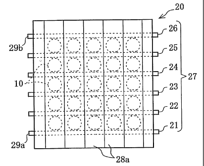
that uses twenty-five semiconductor devices 10 disposed in 5 rows and n
columns, for example. The light receiving semiconductor module 20
comprises twellty-#ive scmiconductor devices 10; a conductive connection
mechanism 27 which comprises six connectiug leads 21 to 26 and electrically
connects the twenty-five semiconductor devices 10~ a light transmitting
member 28; and a positive terminal 29a and a negative terminal 29b.
The twenty-fivo granular semiconductor devices 10 are disposed in
five rows and five colunuis in a state where the c:onduction direction is
aligned to the direction of'column, a plurality of semiconductor devices 10 of
each column being electrically connectcd in series by the conductive
CA 02456671 2004-02-06
connection mechanism 27 and a plurality of semiconductor devices 10 of each
row being electrically connected in parallel. The conductive connection
mechanism 27 is constituted by six metal'connecting leads 21 to 26. The six
connecting leads 21 to 26 comprise the connecting lead 21 connected to the
positive electrodes 6a on the underside of the semiconductor devices 10 of the
lowernuost row; connecting leads 22 to 25, which are mounted between the
semiconductor devices 10 of each row and the semiconductor devices 10 of the
row adjoining the top face of the semiconductor devices 10 of each row; and
the connecting lead 26 connected to the negative electrode 6b on the top face
of the semiconductor devices 10 of the uppermost row. Each of the connecting
leads 22 to 25 connects the negative electrodes 6b of a lower semiconductor
devices 10 and the pogitive electrodes 6a of an upper semiconductor devices
10. Accordingly, the semiconductor devices 10 of each column are seriallv
connected bv the connecting leads 22 to 25, while the semiconductor devices
of each row are connected in parallel by the connecting leads 21 to 26.
The twenty-five semiconduetor devices 10 and the conductive
connection mechanism 27 are packaged in an embedded state in a light
transmitting naember 28 consisting of a transptzxent synthetic resin such as
an acrylic resin or polycarbonate, for example, a partial cylinder lens
portion.
28a that guides extrinsic light from both sides to the semiconductor devices
10 in each column being formed on the light transmitting member 28. An
electrical circuit that is equivalent to the light receiving seraiconductor
module 20 constittiting this solar cell panel is as shown ,in Fig. 18.
'T'he structure is such that the light receiving semiconductor module
21
CA 02456671 2004-02-06
20 is embedded in the light transmitting member 28 consisting of a
transparent synthetic resin, the twenty-five semiconductor devices 10 and
the connecting leads 21 to 26 are rigidly packaged, and are superior in
strength and durability. The partial cy,linder lens portion 28a of the light
trarismitting member 28 serves to efficiently introduce extrinsic light into
the
semiconductcii devices 10 of each column, and, in comparison with a case
where the surf'ace of the semiconductor module 20 is formed as a flat surface,
possesses wide: directivity and is superior in lighting and light-gathering.
Moreover, tlie refractive index of the light of the light transmitting member
28 is greater than 1.0, and hence the light ent.ering the light transmitting
member 28 is repeatedly reflected at the surface of the partial cylinder lens
portioii 28a and is easily absorbed by the semiconductor devices 10. More
particulaxly, the re$active index of glass and of a transparent synthetic
resin
such as acrylic or polycarbonate is greater than the refractive index of air,
and therefore the incident light from the outside is diffused by the diffused
reflection within the light transmitting member 28 and widely scattered.
The semiconductor devices 10 housed within the light transmitting member
28 are capable of absorbing light in every direction, and hence exhibit high
light usage efficiency in comparison with a solar cell paiiel with a
conventional one-sided flat structure, and generate a large photovoltaic
effect.
Because the semiconductor inodule 20 comprises the
above-raentYoned conductive connection mechanism 27, even when any
semiconductor device 10 exhibits a functional loss or stops functioning due to
~2
CA 02456671 2004-02-06
failure or a shadow, because the output of a normal semiconductor device 10
is output by being shunted via another normal semiconductor devices 10 that
are in a parallel connection, there is hardly any adverse effect caused by the
failure or functional loss of some semiconductor devices 10, which makes the
light receiving semiconductor module 20 superior in reliabi.lity and
durability.
Moreover, a plurality of semiconductor devices 10 can be connected in series
and in parallel via a simple-structure conductive connection mechanism 27.
Next, a method for fabricating the above-described light receiving
semiconductor module 20 (solar cell module) will be described with reference
to Figs. 9 to 15,
Fir3t of all, the above-mentioned nlultiplicity of semiconductor
devices 10 is fabricated and, at the same time, as shown in Fig. 9, the
surface
of a thin plate (about 0.3 mm thick) of an iron-nickel alloy (Fe 56%, Ni 42%)
is
silver-plated or nickel-plated to a thickness of about 3 lzm, and the thin
plate
is punched with a die, whereby the flat-plate-like lead frames 21A to 26A
with four openings 30a and 30b are fabricated. An outer frame portion 31
with a width of about 4 mm and three mutually parallel connecting leads 21
that are 0.5 mm thick, for example, are formed in the lead frame 21A. The
other lead frames 22A to 26A are also formed in this manner.
Next., as showri in Figs. 9 to 13, an aluminum paste 32 (with a
diameter of 0.5 mm, and a thickness of 0.2 to 0.3 mm) is printed at five
points
on the upper surface of the connecting leads 21 to 25 of the lead frames 21A
to
25A respectively, and a silver paste 33 (with a diameter of 0.5 mm and a
thickness of 0.2 to 0,3 inin) is printed at five point.s on the lower surface
of the
23
CA 02456671 2004-02-06
connecting leads 22 to 26 of the lead frames 22A to 26A respectively. Next,
semic.onductor devices 10 are placed, with keeping the positive electrodes 6a
downward, on the aluminum paste 32 of the respective connecting leads 21 of
the lead frames 21A. Next, the lead frame 22A is placed on the fifteen
semiconductor devices 10 of the first row, and the fifteen negative electrodes
fib are caused to make contact with the silver paste 33 of the connecting lead
22. Thereafter, as described above, the lead frames 23A to 26A and
semiconductor devices 10 are sequentially placed, and, the lead frames 21A to
26A. are used to place 25x3 semiconductor devices 10 in the form of the 3 sets
of 5X5 matrices shown in Fig. 13, whereby an assembly body 30 is made.
Thereafter, in a state where a predetermined weight is placed on the
uppermoat-level Iead frame 26A, the aluminum paste 32 and the silver paste
33 are cured by being housed within the heating oven and heated at a
temperature of about 160 to 180 C.
Accordingly, the twenty-five semiconductor devices 10 of each set
(each module) are electrically connected via the six lead frames 21Ato 26A, so
that a total of 75 semiconduct.or devices 10 of three sets are contained in an
orderly fashion between the connecting leads 21 to 26 of the six lead frames
21A to 26A. The twenty-five sezaiconductor devices 10 of each module 20
thus assume a stat.e where the semiconductor devices 10 of each column are
electrically connected in series by the connecting leads 21 to 26 and where
the
semicoxiduct.or dev;ces 10 of each row are electrically connected in parallel
by
the connecting lead S 21 to 26.
Next, as shown in f'igs. 14 to 15, the assembly body 30 of seventy-five
24
CA 02456671 2004-02-06
aemiconduc:tor devices 10 and six lead frames 21A to 26A is housed within a
mold (not illustrated) and molded as shown by using a transparent syntheti.c
resin (such as acrvlic resin or polycarbonate, for example). The
semieonductor devices 10 in 5 rows and 5 columns of each set together with
the corresponding conriecting leads 21 to 26 are embedded within the light
transmitting member 28 and packaged by the light transmitting member 28.
Three sets of light receiving semiconductor modules 20 constituting solar cell
panels are thus molded at the sanre time. Apartial c_ylinder lens portion 28a,
which focubes extrinsic light from both sides onto the semiconductor devices
in each column, is formed on the light transmitting member 28. Further,
the two ends of the connecting leads 21 to 26 protrude to the outside of the
light transmitting member 28.
Finally, when the three sets of light receiving seniiconductor modules
are decoupled froin the outer frame 31 of the six lead frames 21A to 26A,
the light receiving semiconduct.or modules 20 shown in Figs. 16 and 17 are
obtained.
<First Modified Embodiment>
In this embocliment, a description is made for an example in which
the assernbly body 30 is assembled after the positive electrode 6a and the
negative electrode 6b have been formed on each semiconductor device 10.
However, as will be described next, the positive electrode 6a and the negative
electrode 6b could also be formed during the assembly of the assembly body
30. That is, the aluniinum paste 32 (with a diam.eter of 0.5 rnlxi and a
CA 02456671 2004-02-06
thickness of 0.2 to 0.3 min) is printed as shown in Fig. 10 at five points on
the
upper surface of the connecting leads 21 to 25 of each of the lead frames 21A
to 25A, and the flat surface 2 of the semiconductor device 10 not formed with
electrodes is made to make surface contact atop the respective aluminum
paste 32. In this state, the lead frames 21A to 25A together with the fifteen
semiconductor devices 10 on the lead frames 21A to 25A are heated to 150 C
in a heating oven so as to cure the aluminum paste 32, whereby the
semiconductor devices 10 are made to adhere to the connecting leads 21 to 26.
Next, silver paste 33 (with a diameter of 0.5 mm and a thickness of
0.2 to 0.3 mm) is applied to the respective apex (the apex opposite to the
flat
surface 2 such that the center of the semiconductor device 10 is interposed
therebetween) of the fifteen semiconductor devices 10 stuck to the lead
t'raines 21A to 25 A, and the corresponding lead frames 22A to 26A atop the
fifteen semiconductor devices 10 of the lead frames 21A to 25A respectively
(the lead frames 22Ato 25Ato whose upper side the semiconductor devices 10
are stuck, and the lea(i fzame 26A to vvhich a semiconductor device 10 is not
stuck) are placed vaith the two edges of the outline of the lead frames 22A to
26A serving as a reference. The connecting leads 22 to 26 are assembled in
the assemblv body 30 shown in Fig. 13 by being made to contact the silver
paste 33. 'I'he a.ssezubly body 30 is then heated to 150 C in a heating
furnace
to cure the silver paste and to stick the semiconductor devices 10 to the
connecting leads 22 to 26.
Next, the assembly body 30 is housed within the heating furnace and
heated for approximately 30 minutes at a temperature of 800 to 850 C in a
26
CA 02456671 2004-02-06
nitrogen atmosphere. As a result of this heating, the diffusion-mask thin film
of each semiconductor device 10 is destroyed by the heat and the aluminum
paste enters a state of being connected to the p-type silicon semiconductor,
such that the aluminum paste forms the positive electrode 6a. At the same
time, the antireflection film 7 of each semiconductor device 10 is destroyed
by
the heat and the silver paste enters a state of being connected to the n type
diffusion layer 3, whereby the silver paste forms a negative electrode 6b.
Accordingly, the assembly body 30 shown in Fig. 13 is then finished. With
this method, the step of forming each semiconductor device 10 with the
positive and negative electrodes 6a and 6b is omitted, it will be possible to
form the electrodes 6a and 6b in parallel with the assembly of the assembly
body 30. This is therefore advantageous on account of the reduction in the
costs of fabricating the semiconductor module 20.
<Second NZodified Embodiment> (see Figs, 19 and 20)
In this embodiment. the asseinbly body 30 is housed within a mold
and three 5ety' worth of semiconductor modules 20 are molded bv pouring a
transparent synthet.ic resin into the mold, whereupon each semiconductor
module 20 is decoupled from the outer frame 31. However, three sets' worth
of semiconductor modules 20 need not necessarily be molded in this manner.
As showii in Figs. 19 and 20, the twenty-firre x three semicoriductor devices
and the connecting leads 21 to 26 are housed within a mold with a
cube-shaped mold cavitv and a transpar6nt 5ynthetic resin is poured into the
xnold and solidifies such that a cube-shaped semiconductor module 20A in
27
CA 02456671 2004-02-06
which the seventy-five semiconductor devices 10 are three-dimensionallv
housed in a substantially cube-shaped light transmitting member 28A may
be molded. Further, a partial cylinder lens portion 28a like the
above-mentioned partial cylinder lens portion 28a is desirably formed on the
outside of the cube shaped semiconductor module 20A. So too in the case of
the semiconductor module 20A, although, in order to simplify the description,
the same was made by taking, as an example, a case where the
semiconductor devices 10 are arranged in a five row by five column matrix,
there are also cases where the semiconductor devices 10 are arranged in the
form of a matrix of multiple rows and multiple columns and this matrix is
then molded to form the cube-shaped semiconductor module 20A.
In the case of the cube-shaped semiconductor module 20A, the
multiple semicoriductor devices 10 are arranged three-dimensionally in the
light transmi.ttiiig member 28A, and hence light from every direction within
three dimensions is received and photoelectrically converted. Moreover,
because this multiplicity of semiconductor devices 10 has a large surface area
for receiving light, this multiplicity of semiconductor devices 10 possesses a
light receiving capacity that is large in comparisori with the semiconductor
module 20. A portion of the light entering the light transmitting member 28A
reaches directly to the serially connected semiconductor devices 10, while the
remaii-iing light reaches to the 5erniconductor devices 10 after repeatedly
undergoing diffused reflection and scattering. For this reason, the light
usage efficiency can be remarkably improved than a conventional solar cell
panel. Further, the cube-shaped semiconductor module 20A can be
28
CA 02456671 2004-02-06
constituted in the form of a sheet and a semiconductor module with a
structure in which the semiconductor devices 10 are incorporated in a
plurality of layers within a transparent and flexible light transmitting
member can also be implemented.
<Third Modified Embodiment> (see Figs. 21 and 22)
Next, a description will be provided for a Ynodified embodiment of the
semiconductor module with a light receiving function that utilizes the
semiconductor device 10, As shown in Figs. 21 and 22, this semiconductor
module 40 comprises eighty (16x5) semiconductor devices 10, for example,
which #uiYCtion to perform an photoelectric conversion upon receiving lighVa
conduction mechanism 50, which comprises six metal circtilar lead frames 41
to 46; and a light transmitting member 48. However, the semiconductor
devices 10 are the 4ame as the aemiconductor devices 10 of the semiconductor
module 20.
The circular lead frames 41 to 46 are formed integrally with each of
the inside connecting leads 41a to 46a and the outside connecting leads 41b to
46b, and four external leads 41c to 46c. which protrude toward the outside in
the radial direction, are formed on the outside connecting leads 41b to 46b.
F'ortv semiconductor devices 10 are connected to the inside connecting leads
41a to 46a (width 0.8 mm, for example) at equal intervals in the
circumfereiitial direction b5 being grouped into eight columns such that the
conduction direction is uniform by aligxied, and the reniaining forty
semiconductor devices 10 are connected to the outEide connecting leads 41b to
29
CA 02456671 2004-02-06
46b (width 0.8 mm, for example) at equal intervals in the circumferential
direction by being grouped into eight colunin5 such that the conduction
direction is uniforni by aligned.
The conductive connection mechanism 50 comprises a
lowermost-level circular lead frame 41, iniddle=level circular lead frames 42
to 45, and an upperm.ost-level circular lead frame 46. The circular lead
frames 41 to 46 are of the same plate thickness and same quality as the lead
frames (21 to 26) of the above embodiments. An external lead 41c of the
lowermost-level circular lead frame 41 is a positive electrode terminal 47a
and an external lead 46c of the uppermost-level circular lead frame 46 is a
negative electrode terminal 47b.
Similarly to the semiconductor module 20, each of the circular lead
frarnes 41 to 45 is connected by aluminum paste to the positive electrode 6a
of
an upper semiconductor device 10, and each of the circular lead frames 42 to
46 is connected by silver paste to the negative electrodes 6b of a lower
semiconduetor devices 10. Accordingly, the conductive connection
mechanism 50 is such that five semicoriductor devicea 10 of each column are
electrically connected in series, and sixteen semiconductor devices 10 of each
level are electrically connected in parallel.
An assembly body 51, which is produced by assembling the six
circular lead frames 41 to 46 and eighty semiconductor devices 10, is
embedded within the cvlindrical light transmitting meinber 48. However, the
otiter ends of the external leads 41c to 46c protrude to the outside. The
light
t.ransruitting member 48 consists of a transparent synthetic resin such as
CA 02456671 2004-02-06
acrylic or polycarbonate. Conical recesses 48a and 48b, which serve to raise
the light, introduction rate, are formed i.n the nxiddle of the lower and
upper
end faces of the light transmitt.ing member 48. Partial conical chamfered
sections 49a and 49b, which serve to raise the light introduction rate, are
formed on the respective outer circumference of the lower and upper ends of
the light transmitting member 48.
The method of fabricating this yemiconductor module 40 will now be
deseribed. FinSt of all, the circular lead frames 41 to 46 and the eighty
semiconductor devices 10 are fabricated and prepared. Next, substantially
t.he same manner as the semiconductor module 20 was adopted, the assemblv
bodv 51 is assembled by assembling the circular lead frames 41 to 46, the
eight.y semiconductor devices 10, and the aluminum paste and silver paste,
and so forth.
Next, the aluminum paste and silver paste are cured by housing the
assembly body 51 in a heating oven and subjecting the assembly body 51 to a
heat treatment for approximately 30 minutes at a temperature of 800 to
850 C in a nitrogen atmosphere. Next, the assembly body 51 is housed in a
mold, and, when a dissolved transparent sy nt.hetic resin (acrylic resin or
polvcarbonate, for example) is poured into the mold and solidifies, the
semiconductor inodule 40 is obtained.
Further, as per the first modified embodiment, so too when the
semiconductor module 40 is fabricated, the positive and negative electrodes
Ga and 6b may be formed in parallel with the assembly of an assemblv body
60 by using semiconductor devices 10 with no electrode, or inay be formed
31
CA 02456671 2004-02-06
after assembling the assembly body 60.
Because the semiconductor module 40 is formed so as to have a
cylindrical shape as a whole, even in a case where the extrinsic light comes
from any direction within the 360 degrees of the full circumference, thi9light
is reliably introduced to the light txansmitting member 48, and the extrinsic
light from above or below the semiconductor module 40, is also reliably
iritroduced to the light transmitting n-iember 48. The light thus introduced
into the light transmitting member 48 is scattered via diffused reflection
while being pkzotoelectsically converted upon reaching the semiconductor
device 10, thereby generating an electromotive force on the order of
approximately 3.0 volts between the positive electrode terminal 47a and the
negative electrocle terminal 47b,
<Fourth Modilied Embodiment> (see Figs. 23 to 29)
A modified enibodiment of the light receiving sea.niconductor module
will now be described along with the makine~ nrethod and structure thereof.
First of all, the base sheet 60 shown in Fig. 23 is fabricated. The base sheet
60 is a f.7.at-plate=like transparent sheet of a predetermined ;;ize (200 mm x
200 mm, for example) made of a transparent synthetic resin (acrylic or
polycarbonate, for example) with a thickness of 0.4 to 0,6 mm. Square small
holes 61 vvith the.dimensions 1.5 mm x 1.5 mm, for example, which serve to
mount semicoriductor devices 10 like those of the aemiconductor device 10 in
Fig, 8, are formed in the form of a matrix with znultiple rows and multiple
columzis, vertical frames 62 with a width of 0.8 to 1.0 mm being formed
32
CA 02456671 2004-02-06
between one column of small holes and the next column, and connecting lead
formation sections 63 with a width of 0.4 to 0,6 mnil being formed between one
row of small holes and the next row. The sniall holes 61 are desirably formed
having a size and shape such that a plurality of points on the equator midwav
between the positive and negative electrodes 6a and 6b of the semiconductor
devices 10 make light point contact and are trapped. The shape of the small
holes is not restricted to a square. Rather, a variety of shapes can be
adopted.
The base sheet 60 can be fabricated by means of extrusioix molding or
similar by using a precise molding die, but could also be fabricated by boring
with a la9er beam of an excimer laser in a state where predetermined
masking is perfornied on a sheet-like or film-like base sheet member, or may
be fabricated by means of another method.
Next, as shown in Fig. 24, at least a single side of the multiple
connecting lead formation section 63 and sections facing the small holes 61
are formed with a iransparent conductive synthetic resin or a metal
conductive film 64a (with a thickness of 10 to 30 pm, for example), whereby
the connecting lead 64 is produced. A conductive synthetic resin or a metal
conductive film 66a (with a thickness of 10 to 30 pm, for example) is formed
at one end of the base sheet 60 in the column direction thereof and on the
external condiictive wire connection portion 65 at the other end, and the
conductive film 66a is formed in the section facing the small holes 61,
whereby a connecting lead 66 is produced. Further, when the metal
conductiye fil,~ras 64a and 66a are formed, the same may be formed by a nickel
plating film, for exainple. In addition, a multiplicity of semi.conductor
devices
33
CA 02456671 2004-02-06
like those shown in Fig, 8 is fabricated prior to or in parallel with the
fabrication of the base sheet 60.
Next, as shown in Figs. 25 and 26, a semiconductor device 10 is
mounted in each of a multiplicity of small holes 61 in a state where the base
sheet 60 is set in a state of floating approximately 0.5 mm above a suitable
horizontal base plate. In this case, a conductive adhesive or conductive paste
(aluminum paste, silver paste, gold paste, or the like) is applied to the
positive electrode ha and the negative electrode 6b of the semiconductor
device 10, and t.he semiconductor device 10 is mounted in the small hole 61 in
a state where the respective conduction directions of all the semiconductor
devices 10 are uniforrn and where the positive and negative electrodes 6a and
6b make surface contact with the corresponding conductive films 64a and 66a,
the semiconductor device 10 being made to protrude substantially equally
outside both sides of the base sheet 60. Thereafter, where required, the
conductive adhesive and c.onductive paste on the electrodes 6a and Gb may be
cured by being irradiated with laser light.
A conductive connection mechanism that comprises a multiplicity of
coiinecting leads 64 and 66, and a conductive paste, or the like, which
connects the electrodes 6a and 6b of the semicoizductor device 10 to the
connecting leacts, is constituted. As a result of this conductive connection
mechanism, seiniconductor devices 10 of each column are connected in series
and senn.icoriductor devices 10 of each row are connected in parallel.
Next, as shown in Fig. 27, an asseznbl5, body 67, in which the base
sheet 60 and a multiplicity of semiconductor devices 10 are assenzbled, is
:34
CA 02456671 2004-02-06
housed. within a predetermined mold, and, when molding is performed by
pouring a dissolved transparent synthetic resin (acrylic, polycarbonate, or
the like, for example) into the mold, the base sheet 60 and the multiplicity
of
semiconductor devices 10 are embedded within a light transmitting rnember
68 consisting of a synthetic resin, whereby a substantiall,y transparent sheet-
or fxlul-like 4emiconductor module 70 is obtained. Further, for an external
conductive wire connection, part of an external conductive wire connection
portion 65 at both ends of the base sheet GO is molded in a state of
protruding
from the light transmitting member 68.
The average film thickness of the synthetic resin applied during this
,moldirsg may be 0.5 to 1.0 mm, for example, but is not limited to this film
thickness. Rather, the film thickness can be determined freely. As for the
synthetic resin provided in the molding process, a synthetic resin of the same
type as the base sheet 60 is desirably adopted. However, a different type of
synthetic resin may also be adopted, and, by suitably selecting the synthetic
resin provided in this znolding, a flexible semiconductor module 70 can also
be rendered. Further, when a conductive paste is adopted for the positive and
negative electrodes 6a and 6b of the semiconductor device 10, curing of the
conductive paste can also be achieved by means of the heat of the synthetic
resin injected during molding.
In the case of the semiconductor module 70, in order to raise the light
introduction capacity ( I lighting=gatheririg capacity), molding is performed
such that the outside part corresponding with the semiconductor devices 10
of each colunuz is a partial cylinder face 69. 'T'he partial cylinder face 69
may
CA 02456671 2004-02-06
be formed only on one side, while the other side may be formed as a flat
surface, Further, molding may be perf'ormed such that the outside part that
corresponds with each semiconductor device 10 of the semiconductor module
70 is a partial-sphere surface. The partial-sphere surface may be formed on
only one side, while the other side may be formed as a flat surface.
Here, as shown in Fig. 28, two assembly bodies 67 are placed close
together parallel to each other by being shifted tiy a half pitch in the row
direction and/r7r column direction. In this state, the assembly bodies 67 are
housed in a mold as described above, and, when a light transmitting member
68A is formed as a result of the asseanbly bodies 67 being integrally molded
by using a transpatent synthetic resin, a semiconductor module 70A is
obtained. Further, in the case of the semiconductor modules 70 and 70A, an
optical reflection film such as a nickel plating film mav be formed on the
outside ori the opposite side to the entering direction of the incident light.
According to the semiconductor modules 70 and 70A of this
embodiment, in addition to actions and effects like those of the semiconductor
modules 20, 20A, 40, being obtained, specific actions and effects are also
obtained. 'I`he seiniconduct.or modules 70 and 70A. are fabricated in sheet
form by forining connecting leads 64 and 66 on the base sheet 60, which can
be fabricated at low cost, niounting a multiplicity of semiconductor devices
10,
and then forniing synthetic-resin light transmitting xcteinbers 68 and 68A by
means of injec ion molding and so forth. Hence, a sheet-like or film-like
lightweight semiconductor module is pxoducect, fabrication costs can be
reduced, and a high output or high voltage photovoltaic effect can be
36
CA 02456671 2004-02-06
generated by means of a multiplicity of semicaiiductor devices 10.
The semiconductor modules 70 and 70A can also be fabricated with a
thickness of 2.0 to 3.0 mm, and a solar cell panel (solar cell sheet) that can
be
st:uck on window glass can also be implemented. Moreover, flexible
semiconductor modules 70 and 70A. can also be constituted, it will be possible
to fabricate semiconductor modules -, 0 and 70A that can be applied to a
varietV of applications such as a semiconductor module that can be mounted
on the body surface of ari automobile.
More particularl,v, where the semicondtzctor module 70A is concerned,
because semiconductor devices arranged in a matrix shape are incorporated
in a two-layer st.ructure, light entered in the light transmitting member 68A
is easily absorbed by the semiconductor device 10, thereby raising the light
usage efficiency.
Next. an example in which this inodified embodiLnent is modified in
par.t will be described sinipl,y on the basis of Figs. 29 and 30. As shown in
Figs. 29 and 30, a multiplicity of substantially semispherical small recesses
72 are formed in the form of a matrix with znult.iple rows and multiple
colurnns on a base sheet 71 (with a thickness of 1.5 to 2.0 mm, for example)
made of a transparent synthetic resin such as acrylic or polycarbonate, for
example. An optical reflection film 73 such as a nickel plating film, for
exaraple, may be forixied, on the rear side of the base sheet 71. But the
optical
reflection film 73 xuay be omitted. Further, the base sheet 71 may be
constituted by a soft transparent synthetic resin material.
The small recesses 72 are formed such that half of the semiconductor
37
CA 02456671 2004-02-06
devices 10 on the one side can be fitted at a minute gap or without a gap, and
are formed with af1at section 72a that conforms with the shape of the flat
surface 2 of the semiconductor device 10. Further, retaining portions 74,
whieh qerve to provide a hold, by way of surface contact with the positive and
negative electrodes 6a and 6b, are formed so as to protrude upright
approximately 0.4 mm to the front side of the page of Fig. 29, at both ends of
the small recesses 72 in the column direction thereof. Multiple row
coniiecting leads with the same structure as the connecting leads 64 and 66
are formed on the base sheet 71 and the semiconductor devices 10 are
mounted in each of the small recesses 72, such that the positive electrodes 6a
and negative electrodes 6b are connected to corresponding connecting leads
so as to be capable of conducting electricity thereto, and are f"Sxed firrnly,
Here, the constitution may be such that the retaining force of the retaining
portions 74 is used to retain the semiconductor devices 10. Further, in order
to facilitate the forniation of the connecting leads, the retaining portions
74 of
each row m ay be f'orzxted continuously. Similarlv to the connecting leads 64
and 66, the connecting leads formed in multiple rows constitute a conductive
connection mectianism whereby the multiplicitv of semiconductor devices 10
of each column are connected in series and the semiconductor devices 10 of
each row are connected in parallel.
Next, an assembly body 75 that is produced by mounting a
mult.iplicitv of semiconductor devices 10 on the base sheet 71, is housed in a
predeterniineci mold and molding is perforined by pouring a transparent
synthetic resin into the mold. A transparent and soft svnthetic resin material
38
CA 02456671 2004-02-06
may be used as the synthetic resin provided in this molding. Accordingly, a
multiplicity of semicon.ductor devices 10 become a state of being embedded in
a light transmitting member 77 that consists of the base sheet 71 and a
synthetic resin 76 that is poured into the mold and solidifies. A lightweight,
light receiving semiconductor module 70B (solar cell sheet, solar cell film,
or
solar cell p anel} that is in the form of a sheet or film is thus obtained.
Further,
a partial cylinder surface that is similar to the partial cylinder face 69, or
a
partial-sphere surface, or the like, may be forined in the outer surface of
the
light transmitting merz-iber (76) that is formed by the molding. V67ith the
semiconductor module 70B, actions and effects like those of the
semiconductor modules 70 and 70A are obtained.
<Fifth Modified Embodiment> (Figs. 31 to 34).
Fig. 34 is a cross-sectional view of a semiconductor device 80
constituting a spherical light receiving cell. The fabrication method and
structure of the semiconductor device 80 will now be described on the basis of
Figs. 31 to 34.
I'he semiconductor element 81 shown in Fig. 31 is the sanie as the
semiconductor element 1 shown in Fig. 5. One flat sttrface 83 is formed on a
spherical p-type silicon single crystal 82, and, before a thin=film n+ silicon
growtli layer 85 is grown on the surface of the silicon single crystal 82, a
mask thin film 84 (silicon oxide film), which serves as a mask during the
browth of the thin=film single crystal, is formed in the same iuanner as in
the
above embodiment on the flat surface 83 and in the vicinity thereof. Further,
39
CA 02456671 2004-02-06
where required, a silicon nitride film (SisN4) may be formed on the outside of
the mask thin filn-t 84.
Next, as shown in Fig. 32, an n+ type growth layer 85 (this is
equivalent to a semiconductor thin-film deposition layer) with a uniform film
thickness (for example, 0.5 to 1.5 Ia.rn.) is grown on the surface of the
externally exposed p-type silicon single crystal 82 by using hot-wall type
atmospheric pressure Chemical Vapor Deposition (CVI)) in which the source
gases are known dichlorosilane (SiH202) and monosilane (SiHa), for example.
Accordingly, a spherical pn junction 86 is formed at the surface of the p-type
silicon single crystal 82. Next, the mask thin film 84 is removed by using a
known etching method and then the whole surface is lightly etched (with a
thickness of 0.1 to 0.2 ttm,, for example). Thereafter, a silicon oxide film
with
a thickness of 0.4 to 0.5 lim is once again deposited (formed) and, as shown
in
Fig. 33, a sttbstantially spherical antireflection film 87 is formed.
In addition to a silicon oxide film, a thin film of titanium oxide, silicon
nitride, aluminum oxide or magnesium fluoride, or the like, can also be
adopted as the antireflection film 87.
Next, similar to the above embodiments, a positive electrode 88a and
a negative electrodw., 8131) are formed in the middle of the flat surface 83
and at
the apex of the spherical surface facing the tlat surface 83 respectively,
such
that the center of the semiconductor element 81 is iilterpoRed therebetween.
This semicoriductor device 80 (a spherical-surface light receiving cell) also
affords substantially the same photoelectric conversion function as the
semiconductor device 10 in Fig. 8, and possesses wide directivity.
CA 02456671 2004-02-06
<Sixth Modified Embodiment> (see Figs. 35 to 38)
Fig. 38 is a cross-sectional view of an npn phototransistor 90
(semiconductor device) that has a substantially spherical light receiving
surface. A description of the making method and structure of this iipn
phototransistor 90 will now be made on the basis of Figs. 35 to 38.
The semiconductor element 91 shown in Fi,g. 35 is an element
produced by forming a flat surface 93 at one apex of the spherical n-type
silicon single crystal 92 (resistivity 1 to 10 Q cm), and then forming a boron
diffusi.on mask thin film 94 (silicon oxide film) on the flat surface 93 and
in
the vicinity thereof The semiconductor element 91 differs only in that the
n-type silicon single ervstal 92 is applied in place of the p-type silicon
single
crvstal in Fig. 5 of the above embodiment, and can therefore be fabricated in
substantially the same manner as the semiconductor element 1 in Fig. 5.
Next, a p-type base layer 95 is formed ozx the surface of the n-type
silicon single crvatal 92 by diffusing boron (to a depth of 0.3 to 0.6 pin,
for
example), which constitutea the p type impurity, by known thermal diffusion.
Accordixigly, a substantially spherical collector junction 96 is formed
between
the p t.vpe base layer 95 and an n-type collector 92a consisting of the n-type
silicon single crystal 92. A thin silicon oxide film 97, which is generated
when
the boron is diffused, is removed by means of a known etching technique
together with the diffusion mask thin filni 94. Thereafter, as shown in Fig.
37,
silicon oxide films 98 and 98a are provideci once again over the whole
surface.
In order to use sili.con oxide film 98 as a mask for the phosphorus diffusion
on
41
CA 02456671 2004-02-06
top of' the surface of the p-type base laver 95, and the silicon oxide film 98
is
removed by a known photoetching technique, leaving the silicon oxide film
98a on the flat surface 93 and in the vicinity thereof. Further, the flat
surface
93 can be used to align the part to be masked.
Next, a substantially spherical n-type emitter layer 99 is formed in
the region of the p-type base layer 95 by diffusing phosphorus (to a depth of
. pe impurity by means of
0. 1 to 0.2 kim, for example) which constitutes the n=tv
known thermal diffusion techniclue. A.ccordingly, as shown in Fig. 37, an
emitter junction 100, which keeps a fixed interval (for example, 0.1 to 0.4
pm)
from the collector junction 96, is formed between the n-type emitter layer 99
and the p-type base layer 95. The thin silicon oxide film generated during the
phosphorus diffusion is used as an antireflection film 101. Next, a collector
electrode 102 and an emitter electrode 103 are provided as shown in Fig. 38
by using a silver paste and an aluminuixi paste as used for the semiconductor
elenotent 1 of the above embodiments. The electrodes 102 and 103 may be
formed so as to be usable as a junction with an external electrically
conductive membei such as a lead frame.
The yubstantially spherical npn phototransistor 90 (equivalent to a
light receiving serniconductox device) has a spherical surface of which the
majority is a light receiving surface, such that when incident light from
autside is absorbed in the vicinity of the collector junction 96 in a state of
reverse bias, an optical current is generated and an amplified external
ctirrent flows between the emitter electrode 103 and the collector electrode
102. This phototransistor 90 can be used as an optical switch or the like and
42
CA 02456671 2004-02-06
has characteristics such as high light receiving sensitivity and wide light
directivity.
Next, descriptions will be made for various modified embodiments
partially modifying the above embodiments.
1) A silicon polycrystal can also be adopted as the semiconductor
constituting the semiconductor elements 1, 81, 91, or, instead of silicon,
another semiconductor. such as an Si and Ge mixed-crystal semiconductor, or
a multilayered structure semiconductor may be adopted, for example. Any
compound semiconductor such as GaAs, InP, GaP; GaN, InCuSe, or SiC may
be adopted and another semiconductor may be applicable,
2) The diameter of the semiconductor crystal forming the
semiconductor element 1 is not limited to 1.5 mm. Rather, there are also
cases where the cliameter has a magnitude on the order of 0.5 to 3.0 mm.
Further, the conductivity type of the semiconductor crystal forming t.he
semic;onductor element 1 is not restricted to the p-type. The n-type is also
acceptable, in which case a p-type diffusion layer is formed.
3) The diffusion layer 3 and the pn junction 4 can also be formed by
using another semiconductor thin-film deposition method such as Chemical
Vapor Deposition.
4) The antireflection film 7 may be constituted by another insulating
film such as a titanium oxide film or a silicon nitride film, in place of
asi.licon
oxide film. 5) Either one or both of the electrodes 6a and Gb can be formed by
using any electrode material such as gold, silver, copper, aluzninum,
antimony,
43
CA 02456671 2004-02-06
an alloy of antimony and gold, gallium, an alloy of gallium and silver, and an
alloy of gallium an(i gold, and by using a paste of such material.
6) In place of the light transmitting xuember of the semiconductor
module 20 and 20:3., a structure, which is formed by mounting reinforced
glass plates on both si(ies of the semiconductor module, causing a
transparent Ethylene Vinyl Acetate (EVA) resin or the like to fill the area
between the reinforced glass plates, and then sealing the ends by means of a
frame, could also be adopted.
7) The quantity. disposition, and form of the semiconductor devices
mounted in the semiconductor module 20, 20A, 40, are not restricted to those
of the above embodiments and can be set freely. For example, it is also
possible to obtain a sezniconductor module with a flexible, sheet-like
structure by motiintiiig a multiplicity of semiconductor devices in multiple
rows and znultiple colurnns on a thin sheet inade of a transparent synthetic
resin (with a thickness of 0.3 mm, for example), by connecting the
multiplicity of semiconductor devices of each column in series and the
semiconductor device5 in each row in parallel by means of a con.ductive
connection mechanism, and then molding a light transmitting member film
ozi both sides of the sheet, Further, so too with the sheet=like
seiniconductor
module, the semiconductor devices 10 can also be disposed in a plurality of
lavers.
8) The semic.onductor module has been described by taking the
example of a seiniconductor module with a light receiving function. However,
the semiconductor module of the present invei-ition can also be applied in the
44
CA 02456671 2004-02-06
same manner to a semiconductor module with a light emitting function.
I-lowever, in this case, a semiconductor device with a light emitting function
(a spherical semiconductor device, cylindrical seiniconductor device, or
granular semiconductor device) must be applied as the semiconductor device.
A variety of spherical light emitting diodes proposed by the inventors
of the present invention in patent publications tti'098/15983 and
W099/10935, and so forth, for example, can be applied as such a
semiconductor device with a light emitting funct.ion. Light emitting diodes
with other types of structure could also be adopted. Such a semiconductor
module with a light emitting function can be applied to a planar
light-emission type lighting device, a monochrome or color display, or various
display devices, and so forth.
9) Moreover, the person skilled in the art is capable of implementing
ather embodiments made by applying a variety of modifications to the above
embodiments without departing from the spirit of the present inveiition. The
present invention is therefore not restricted to the variety of embodiments
disclosed in the above embodinlents.