Note: Descriptions are shown in the official language in which they were submitted.
CA 02456765 2004-02-04
WO 03/014722 PCT/US02/25019
NUCLEIC ACID FIELD EFFECT TRANSISTOR
[0001] The present invention relates to the detection of hybridization of
nucleic acid
and more particularly to electronic devices for detecting hybridization of
nucleic acid.
CROSS-REFERENCE TO RELATED APPLICATIONS
[0002] This application claims the benefit of U.S. Provisional patent
application
Serial No. 60/310,992 filed on August 8, 2001 and entitled "DNA Field Effect
Transistor"
and incorporated by reference herein.
STATEMENT REGARDING FEDERALLY SPONSORED RESEARCH
[0003] This invention was made with govenunent support under Grant No. DMR-
9632635 awarded by the National Science Foundation and Grant No. N00014-98-
0594
awarded by the Office of Naval Research.
BACKGROUND OF THE INVENTION
[0004] The human genome project has accentuated the need for rapid
identification of
the expression of particular genes in particular cells or organisms. The most
promising
technology for parallel detection is based on so called "genechips" (see
"Light-generated
oligonucleotide arrays for rapid DNA sequence analysis." Pease, Solas, et al.,
Proc. Natl.
Acad. Sci. (USA) 91:5022-5026, 1994; Fodor, Science 393, 1997). "Genechips"
consist of
arrays of spots of oligonucleotides attached to a solid (e.g., glass)
substrate. Photo-
deprotection and optical lithography permit many thousands of spots, each
corresponding to a
unique DNA sequence, to be "printed" onto a square-centimeter sized chip by
the use of one
mask for each base at each step of polymerization, so that an enormous number
of sequences
may be printed in just a few steps.
CA 02456765 2004-02-04
WO 03/014722 PCT/US02/25019
[0005] The genechip is usually incubated with fluorescently labeled target DNA
and
then rinsed. Hybridization is detected by fluorescence at the sites where
target DNA (and its
associated fluorescent tag) has bound. This detection scheme therefore relies
on an
intermediate step in which the target is combined with one or more fluorescent
labels. For
example, gene expression might be monitored by collecting the expressed mRNA
and
translating it to cDNA which is, made from a labeled primer. After
hybridization, the chip is
illuminated with light that excites the fluorescent molecules and the location
of the
fluorescent spots is determined by confocal microscopy. Automated systems for
doing this
readout step are commercially available from Molecular Dynamics and Hewlett-
Paclcard.
They utilize automated image analysis of the illuminated, hybridized arrays to
generate a map
of the location of the hybridized DNA, and thus identify the target DNA. This
approach is
indirect. The optical readout step must be followed by image analysis and
processing before
the target DNA is identified, greatly complicating the readout process.
Furthermore, the
present approach requires labeling of target DNA.
[0006] It would be desirable to use electronic means to detect hybridization
of target
DNA with probe DNA, making the whole process capable of direct interfacing to
a computer.
In principle, this is a simple task, because the linear charge density
associated with double
stranded DNA is twice that of single stranded DNA. Even in the presence of
screening
counter ions, the change between single and double stranded DNA produces a
significant
time-averaged difference in local charge density. Near a depleted
semiconductor surface, this
change in charge density (or, correspondingly, surface potential) causes
changes in a
depletion layer near the semiconductor surface. This effect is exploited in a
scanning probe
potentiometer designed to locate regions of local change in charge density,
such as tethered,
hybridized DNA (Manalis, Minne, et al., Proc. Natl. Acad. Sci. (USA) 91:5022-
5026, 1999).
In the device described by Manalis, et al. (Manalis, Minne, et al., s-upra,
1999) photo-current
-2-
CA 02456765 2004-02-04
WO 03/014722 PCT/US02/25019
from a small depleted region at the apex of a scanning probe is detected.
Changes in charge
density near the apex of the probe signal variations in charge. The device is
designed to be
scanned over a surface to which molecules are tethered, detecting
hybridization of DNA, for
example, as a local change in charge density.
[0007] In principle, the same approach could be used with a field effect
transistor
(FET), if the conducting channel could be exposed so that oligonucleotides
could be attached,
and changes in charge density detected as hybridization is carried out with
target molecules.
However, conventional FETs have gate electrodes covering the conducting
channel. These
not only obscure the channel, but they also require connections to be bought
into the region
of the device above the channel, malting it incompatible with exposure of the
channel to
solutions.
[0008] The need for such a device goes beyond DNA hybridization. Any
interaction
that changed the charge associated with a biopolymer could be detected by such
a device.
Examples would be changes in oxidation state of a redox protein or binding by
one
polypeptide to another where there is a net change of charge.
[0009] Accordingly, it is an object of the present invention to provide a
device for
direct, electronic detection of biopolymer binding, such as DNA hybridization,
compatible
with the solution chemistry required for carrying out the binding. It is
another object to
eliminate the need of labeling of either the probe or target DNA. It is
another object to
construct a field effect transistor compatible with exposure to solutions both
for attachment of
DNA and for subsequent detection of hybridization.
SUMMARY OF THE INVENTION
[0010] The present invention is a field effect transistor (FET) formed from a
silicon-
on-insulator layer on top of a semiconducting substrate. The silicon-on-
insulator layer is
-3-
CA 02456765 2004-02-04
WO 03/014722 PCT/US02/25019
separated from the substrate by a buried oxide layer. Drain and source
electrodes are
attached to the top silicon-on-insulator layer, which forms the conducting
channel of the FET.
An electrode is attached to the substrate, so that the substrate can be used
as a back-gate to
control the conductivity of the silicon-on-insulator channel. The top silicon-
on-insulator
layer is protected by an oxide layer, into which windows are etched to expose
the surface of
the silicon-on-insulator layer. When this surface is exposed to air a thin
native oxide layer is
formed. DNA oligomers or other nucleic acid biopolymers are attached to this
thin native
oxide layer in the window within the thiclcer protective oxide layer.
Hybridization of the
nucleic acid biopolymer is detected from the consequent shift in threshold
voltage, or a shift
in current at a given back-gate (Vb~) and drain (Vds) bias. Hybridization is
detected from the
consequent shift in threshold voltage, or a shift in current at a given back-
gate to -source bias
(Vbg) and source-to drain bias (Vds).
[0011] These and other aspects of the invention will become apparent from the
following description. In the description, reference is made to the
accompanying drawings
which form a part hereof, and in which there is shown a preferred embodiment
of the
invention. Such embodiment does not necessarily represent the full scope of
the invention
and reference is made therefore, to the claims herein for interpreting the
scope of the
invention.
BRIEF DESCRIPTION OF THE DRAWINGS
[0012] Fig. 1 is a schematic layout of the back-gated FET constructed in
accordance
with the present invention.
[0013] Fig. 2 is a schematic layout of a back-gated FET with source and drain
connections in place and a protective layer and window opening above the
channel.
-4-
CA 02456765 2004-02-04
WO 03/014722 PCT/US02/25019
[0014] Fig. 3 is a schematic layout of the back-gated FET with biomolecules
attached
to the native oxide layer above the channel.
[0015] Fig. 4 illustrates one scheme for covalent attachment of DNA to a
native
silicon oxide.
[0016] Fig. 5 is a chart illustrating current vs. gate-source bias for a baclc-
gated FET
with, and without an organic monolayer attached.
[0017] Fig. 6 is a schematic illustrating control elements used to correct for
systematic changes in electrical output characteristics of the FET due to
factors other than
molecular binding.
[0018] Fig. 7 is a chart illustrating the source to drain current in a FET
constructed in
accordance with Fig. 3 when each of a non-hybridizing and a hybridizing DNA
are applied.
DESCRIPTION OF THE PREFERRED EMBODIMENTS
[0019] The current invention in its preferred embodiment is based on a back-
gated
field effect transistor (FET), shown schematically in Fig. 1. Basically, the
back-gated FET
comprises a semiconductor layer provided on an oxide insulating layer which
is, in turn,
provided on a conductive gate. The gate is therefore located on the baclc of
the FET, as
opposed to, for example, a MOS~FET in which the gate is on top. The open
semiconductor
layer allows charges in a fluid placed on or in the semiconductor to interact
with the
semiconductor, as described below.
[0020] Referring still to Fig. l, the FET as shown is built on a silicon on
insulator
(SOI) wafer available commercially from Ibis Corporation of Danvers,
Massachusetts and is
manufactured using a separation by implanted oxygen (SIMOX) process. Other
sources and
arrangements for the manufacture of silicon-on-insulator wafers are readily
apparent to those
slcilled in the art, including wafer bonding and etch back as well as the
SmartCutTM process.
-5-
CA 02456765 2004-02-04
WO 03/014722 PCT/US02/25019
The FET consists of a layer of silicon 10 on top of a buried oxide (BOX) layer
20 that is, in
turn, located on a silicon wafer 30 that serves as the substrate. The
intrinsic surface layer of
silicon 10 is typically 0.03 to 1 microns in thickness and the BOX layer 20 is
typically 0.1 to
1 microns in thickness. Individual devices are isolated from each other by
etching through
the surface silicon layer 10, down to the BOX layer 10. The unetched areas of
the surface
silicon layer 10 are used to form the active regions of the device. The
etching can be
performed by wet chemical etching or reactive ion etching, as is well lcnown
in the art.
Alternatively, the devices can be isolated using a well-known process called
local oxidation
of silicon (LOCOS). During LOCOS, the regions of the surface silicon layer 10
that are not
required for the active regions are oxidized and the silicon in these regions
is converted to
insulating Si02.
[0021] In a preferred embodiment of a field effect transistor device
constructed in
accordance with the present invention, an n-channel inversion layer 65 is used
to carry
current between n-type source 40 and n-type drain 50 contacts as is shown in
Fig. la. For this
configuration, both the surface silicon layer 10 and the silicon substrate 30
are doped p-type,
with typical doping concentrations in the range 1012 to 1019 Cm 3. Source 40
and drain 50
contacts are heavily doped n-type (e.g. with donor concentrations ND~lOI~-1021
cm 3) using
ion implantation of, for example, phosphorus or arsenic, as is well known in
the art. After
implantation, conventional annealing or rapid thermal annealing at a
temperature in the range
800-1000°C is used to activate the implant and diffuse the contacts to
such a depth that they
reach the BOX layer 20. A p-type substrate or gate contact 55 is required to
apply a back-
gate voltage 60 to the substrate 30. The substrate contact 55 is readily made
by first etching
through the BOX layer 20 down to the substrate 30. The etch step is then
followed by ion
implantation of boron and rapid thermal annealing or conventional amlealing to
activate the
-6-
CA 02456765 2004-02-04
WO 03/014722 PCT/US02/25019
dopants and form a heavily doped p-type region 55 (e.g. with boron
concentration NA~1 O19~
1021 cm 3), as is well known in the art.
[0022] In the absence of an applied bias, this device is intrinsically non-
conductive
because of the lack of an inversion layer in the silicon layer 10 in the
channel 14 between the
source 40 and drain 50 connections. If, however, a bias voltage 60 (Vbg) is
applied between
source 40 and the substrate or gate contact 55 such that the substrate contact
55 is biased
positive with respect to the source 40, minority electrons are attracted to
the interface
between the BOX layer 20 and the silicon layer 10, resulting in the electron
inversion layer
shown schematically by the dashed line 65 in Fig. 1. Thus, current will flow
between the n+
source 40 and drain 50 connections when a bias voltage 70 is applied between
them.
Although the electron inversion layer 65 is formed next to the BOX layer 20
(as opposed to
on the surface of the channel as in a normal FET) it is still extremely
sensitive to charges
placed on the upper surface 75 of the silicon layer 10.
[0023] It will be recognized by those skilled in the art that the same result
may be
achieved by replacing the electron inversion layer 65 with a hole inversion
layer. For the
case of a hole inversion layer an n-type SOI wafer would be used (with a
typical doping
concentration in the range lOlz-lOl~ Cm 3), along with heavily p-type doped
source 40 and
drain 50 contacts (with concentrations in the range of 10'''-1021 cm-3). The
baclc-gate voltage
60 would now be negative with respect to the source 40 contact.
[0024] Referring now to Fig. 1b, in another embodiment of the device current
is
carried between the source 41 and drain 51 contacts via majority carriers and
it is therefore
not necessary to induce a minority carrier inversion layer. For the case of
current flow due to
majority electrons, an SOI wafer with an n-type silicon-on-insulator layer 11
(ND~lOl2-1019
cm 3) would be used and separated from an n-type silicon substrate 31 (ND~lOl2-
1019 cm 3)
by a buried oxide layer 20. The source 41, drain 51 and substrate or gate 56
contacts for this
_7_
CA 02456765 2004-02-04
WO 03/014722 PCT/US02/25019
case would now be heavily doped n-type with a donor concentration of, for
example,
(ND~1019-1021 Cm 3)
[0025] When a bias voltage Vds is applied to the drain 51, current flows in
the silicon
channel 13 and is not necessarily confined to the interface between the
channel 13 and the
BOX layer 20 as indicated by the multiple dashed lines 66. The current flowing
in the
channel 13 can be reduced (increased) by applying a back-gate bias voltage 60
to substrate
contact 56 such that Vbg 60 is less than (greater than) zero. A negative baclc-
gate voltage 10
reduces the electron concentration in the channel 13 and the current flowing
between source
41 and drain 51 can be decreased to zero. Similarly, the current flowing in
chamlel 13 can be
increased by applying a back-gate bias voltage 60 which is greater than zero.
[0026] It will be recognized by those skilled in the art that the same result
can be
achieved in a majority carrier FET in which the current is carried by holes.
In this
configuration both the silicon channel 13 and the silicon substrate 31 would
be p-type and
doped in the range 1012 to 1019 cm 3 and the source 41, drain 51 and substrate
56 contacts
would be heavily doped p-type (e.g. with an acceptor concentration Np~1 O19-1
O21 cm 3),
[0027] Although the FET devices have been described above as constructed using
a
SIMOX wafer, other methods of forming the silicon-on-insulator channel will be
apparent to
those of skill in the art. For example, a poly-crystalline silicon (poly-Si)
or amorphous
silicon (a-Si) layer can also be used. In this embodiment a conventional
silicon wafer is first
oxidized to form a silicon dioxide (Si02) layer of thickness 0.05 to 2 yn on
the surface.
After growth of the Si02, chemical vapor deposition is used to deposit the
poly-Si or a-Si to
form a channel of thiclcness in the range 0.03 to 1 Vim. The processing of the
wafer to add the
source, drain and baclc-gate contact electrodes would then proceed as
described before.
Again, a person skilled in the art will recognize that the poly-Si/a-Si
versions of the device
could be configured in such a way that the current in the silicon-on-insulator
channel flows
_g_
CA 02456765 2004-02-04
WO 03/014722 PCT/US02/25019
through an electron (or hole) inversion layer or an electron (or hole)
accumulation/depletion
layer. Although the electron (or hole) mobility in the poly-Si/a-Si
embodiments of the device
would be substantially less than that in a single crystal SIMOX, or wafer-
bonded or
SmartCutTM SOI wafer, their electrical characteristics would be sufficiently
similar to enable
their use in the electronic detection of DNA hybridization.
[0028] Referring now to Fig. 2, the device of Fig. 1 a is shown encapsulated
in a way
that permits the upper surface 75 of the channel 14 to be exposed to
solutions. Metallic
connections 80, 90, 95 are made by deposition of, for example, aluminum, so as
to contact
the source 40, drain 50 and gate or substrate contacts 55, respectively. The
connections 80,
90, 95 can be deposited by, for example, evaporation or sputter coating as is
well known in
the art. A passivating layer 100 of silicon dioxide or silicon nitride is
applied to a thickness
of between 50 and 1000 nm using standard deposition techniques such as
chemical vapor
deposition or spin-on-glasses. A window 105 is etched into the passivating
layer 100 by
standard lithographic procedures, arranged so as to expose the upper surface
of the SOI 10 in
the channel region between the source 40 and drain 50 diffusions. For example,
one method
of fabricating the window 105 is to use a patterned photoresist as a mask for
a subsequent
etch step using selective acid etches such as hydrofluoric acid, or by
reactive ion etching,
both of which are well known in the art. Ina preferred embodiment, an SU8
resist is used in
order to provide a deep chamlel for fluids contained in the window, as
described below. In
the next step a thin oxide layer 110 is grown over the exposed region of SOI
10. One method
to do this is to exploit the native,oxide that grows naturally on a bare
surface of silicon
exposed to air at room temperature. Alternatively, a thermal oxide layer can
be grown by
heating the silicon to 800-1100°C and exposing the surface to oxygen or
steam. A typical
thiclcness of this layer ranges from 2 nm to 100 nm. Electrical connections
can now be made
-9-
CA 02456765 2004-02-04
WO 03/014722 PCT/US02/25019
to the entire FET 120 consisting of source 80 and drain 50 and back-gate 95 in
any
hermetically-sealed package that has a widow exposing the oxide-coated channel
110.
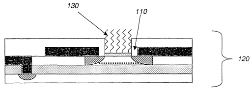
[0029] Referring to Fig. 3, biopolymers 130 are attached to the exposed oxide
layer
110 using suitable chemical procedures, preferably by a covalent bond,
although other
weaker attachments can also be used. The attached biopolymer includes a probe
for
determining hybridization by a target solution, as described below. Preferred
biopolymers
include both synthetic and natural DNA and RNA. Changes in the charge density
associated
with changes in this biopolymer layer will alter the surface potential of the
channel 10
between the source 40 and drain 50 diffusions, and so be detected as a change
in the electrical
properties of the FET. An example of one chemical probe attachment process is
shown in
Fig. 4. Here, a carboxylated DNA oligomer 150 is attached to the oxide layer
110 via a
hydrolyzed silane 140 according to the procedure described by Zammatteo, et
al.
(Zammatteo, Jeanmart, et al., Analytical Biochemistry 280:143-150, 2000). The
OH groups
on the surface of the native silicon oxide layer 110 are naturally present.
Silanizing agents
such as 3'-amino-propyl tri (ethoxy silane) are readily available (from, e.g.,
Sigma Aldrich)
and, on contact with water, or water vapor, hydrolyze to form the compound 140
shown in
Fig. 4. The primary amine reacts with the carboxy group on the DNA to form a
stable amide
bond, and the hydroxyl groups on the silicon compound 140 react with hydroxyl
groups on
the surface oxide layer 110, forming the bound complex 160 shown in the lower
part of Fig.
4. Carboxylated DNA oligomers are available from Midland Certified Reagent
Company
and are synthesized to any desired sequence starting with a carboxy dT.
[0030] There are many other approaches to covalent attachment of DNA to a
silicon
oxide surface. Examples are attachment of aminated DNA (Zammatteo, Jeanmart,
et al.,
su ra, 2000), phosphorylated DNA (Zammatteo, Jeanmart, et al., supra, 2000),
thiolated
-10-
CA 02456765 2004-02-04
WO 03/014722 PCT/US02/25019
DNA (Halliwell and Cass, Analytical Chemistry 73:2476-2483, 2001) and direct
synthesis of
oligomers on the glass surface (Pease, Solas et al., supra, 1994).
[0031] The presence of an organic monolayer on the surface of the channel 110
leads
to large changes in the electrical properties of the electron inversion layer
FET of Fig. la and
Fig. 4 as illustrated in the graph of Fig. 5. Here, bias voltages are applied
to drive the FET
into the active region, and electrical characteristics of the FET are
monitored to determine the
change in electrical characteristics. The graph of Fig. 5 illustrates the
source-drain current
measured at a source-drain bias voltage 70 of 1.0V as a fwction of the source
to back-gate
bias voltage (Vbg) 60 for a bare oxide layer (curve 180) or an oxide layer
with an organic
monolayer attached (curve 190). The shift in threshold voltage, i.e. the
applied back-gate
bias voltage 60 between the source 40 and drain 50 required to cause
measurable current to
flow from the drain 50 to source 40 is about 4V in this case. Changes in the
drain to source
cmTent flow can also be monitored as an indication of changes in the
semiconductor channel.
Even quite subtle rearrangements of the organic layer cause significant
changes to the
threshold voltage 185 of the FET, and these changes are used to detect, for
example,
hybridization of DNA. The voltage shifts depend on the specific chemistry used
to bind the
biopolymer probe 130 to the surface 110 and on the conditions used to achieve
binding (or
unbinding) with the probe 130, but a self calibrated device can compensate for
conditions
used to achieve binding as described below.
[0032] Alterations of electrical behavior caused by changes such as DNA
hybridization are predictable and reproducible if well-controlled and clean
conditions are
used to carry out the reactions. This is not always possible, nor practically
desirable. For this
reason the FET preferably includes control elements as shown in Fig. 6. Here,
a probe 130
comprising DNA is shown attached to the channel oxide 110 of one FET, and the
channel
current is monitored by a current to voltage converter 190, giving a voltage
output 210
-11-
CA 02456765 2004-02-04
WO 03/014722 PCT/US02/25019
sensitive to the state of the probe DNA 130 when the FET is biased
appropriately, i.e.
providing a signal indicative of whether hybridization has occurred. The same
wafer includes
FET devices with blank channel oxides 180 and FET devices with channels
functionalized
with a non-hybridizing DNA sequence 170 selected not to hybridize with
molecules in the
solution being tested. The output of the device is based on differential
measurements made
between the probe device output 210 and the control outputs 220 and 200 as
hybridization (or
conversely, melting) reactions are carried out. Signals provided by the blank
channel 180
normalize for environmental conditions such as salts present, concentrations
of reagents,
temperature, pH, and other factors which affect the characteristics of the
transistors regardless
of whether hybridization has occurred. Signals produced by the non-hybridizing
DNA
sequence channel 120 are used to normalize for effects owing to unspecific DNA-
DNA
interactions other than proper Watson-Crick base repairing. Each of the
outputs 210, 220,
and 230 can be provided to a computer or other device including a central
processing unit
programmed to normalize the output 210 based on the signals at outputs 220 and
230.
Normalization can be provided, for example, using a look-up table, an
algoritlnn, or using
other methods apparent to those of skill in the art.
[0033] Referring now to Fig. 7, a chart illustrating the drain 50 to source 40
current as
a function of time for a FET constructed in accordance with Fig. 2 is shown as
each of a non-
hybridizing target DNA and a hybridizing target DNA are applied to the surface
110
including probe 130, comprising an oligomer. To obtain these results, the open
oxide
window 105 of surface 110 in Figure 2 was exposed to APTES as described above
to produce
the amine-functionalized surface as shown as 140 in Figure 4. An improved
approach
(described in Facci P, Alliata D, Andolfi L. 2002. Formation and
characterization of protein
monolayers on oxygen-exposing surfaces by multiple-step self chemisorption.
Surf. Sci.
504:282-292) was used to attach a probe 130, an amine-modified oligomer as
follows: the
-12-
CA 02456765 2004-02-04
WO 03/014722 PCT/US02/25019
APTES modified window 105, in layer 110, was briefly exposed to a 1mM solution
of
glutaraldehyde to place reactive aldehyde groups on the surface. These are, in
turn, exposed
to a solution of an amine modified oligomer, specifically:
5' Amine-c6 spacer- gatccagtcggtaagcgtgc - 3' (SEQ ID NO: 1)
This is comprised of the following oligomer
gatccagtcggtaagcgtgc
with an amine attached via a 6-carbon allcane spacer. The probe sequences may
be longer
than SEQ ID NO: 1, preferably less than 1 MB, more preferably less than 1 I~B
and most
preferably less than 100 bp. The amine reacts covalently with the
gltuaraldehyde modified
surface to tether the DNA as described above. The resulting device
configuration is as shown
in Figure 3 with the oligomer tethered to the oxide window 110 as the probe
DNA 130.
[0034] The operation of the FET is demonstrated by a plot of drain 50 to
source 40
current versus time of Figure 7. During the measurement an applied drain-
source bias voltage
70 is kept constant at Vds = 1 V and the baclcgate voltage 60 is grounded i.e.
Vbg = OV. A
non-hybridizing target sequence:
5' agttagcatcactccacga 3' (SEQ ID NO: 2)
was introduced to the FET device in a buffer maintained at 80°C (having
previously been
exposed to the heated buffer with no added DNA). The heavy dashed curve marks
the point
-13-
CA 02456765 2004-02-04
WO 03/014722 PCT/US02/25019
at which the target DNA was added, and the current trace 700, shows no
significant response
to the non-hybridizing target DNA.
[0035] The measurement was then repeated with the addition of a hybridizing
sequence:
5' cacgcttaccgactggatc 3' (SEQ ID NO: 3)
A preferable hybridizing sequence has no more than 10% mismatch within the
hybridizing
region. Almost immediately after the hybridizing target DNA is introduced into
the
photoresist opening or window 105 in the oxide layer 110 in Figure 2, the
drain to source
current drops and stabilizes at an approximately constant value, about 4 pA
lower than before
the target DNA is introduced, as shown by the lower curve 710 of Figure 7.
Because the
carriers in the test FET are electrons, the reduction in current is an
expected consequence of
the accumulation of extra negative charge on the oxide as the probe DNA 130
hybridizes
with the target DNA.
[0036] To create a genechip, a plurality of FETS as described above are
constructed
to include a different sequence on each FET, preferably including at least
some FETS that
include a "control" built with a non-hybridizing DNA as described above. When
target DNA
is injected, a computer identifies the sequence based on the electrical
charges of the FET as
described above, and, by analyzing the results can also provide a measure of
the relative
concentrations of the DNA or nucleic acid. Therefore, total gene expression
and relative
level of gene expression can both be mapped.
[0037] It should be understood that the methods and apparatuses described
above are
only exemplary and do not limit the scope of the invention, and that various
modifications
-14-
CA 02456765 2004-02-04
WO 03/014722 PCT/US02/25019
could be made by those skilled in the art that would fall under the scope of
the invention. To
apprise the public of the scope of this invention, the following claims are
made:
-15-