Note: Descriptions are shown in the official language in which they were submitted.
CA 02456769 2004-02-04
WO 03/019656 PCT/US02/26756
INTERCONNECT MODULE WITH
REDUCED POWER DISTRIBUTION IMPEDANCE
TECHNICAL FIELD
The invention relates to interconnect modules for use with integrated circuit
chips.
S BACKGROUND
Mufti-layered interconnect modules are widely used in the semiconductor
industry
to mechanically support integrated circuit chips and electrically attach the
chips to printed
wiring boards. Interconnect modules can be configured to support a single chip
or
multiple chips, and are typically identified by the designation SCM (single
chip module)
or MCM (mufti-chip module).
An interconnect module provides interconnections that serve to electrically
couple
an integrated circuit chip to signal lines, power lines, and other components
carried by a
printed wiring board. In particular, the interconnect module provides
interconnections
that redistribute the densely packed inputs and outputs (I/Os) of the chip to
corresponding
I/Os on the printed wiring board. In addition to electrical interconnection,
an interconnect
module typically serves to mechanically couple a chip to a printed wiring
board, and may
perform other functions such as heat dissipation and environmental protection.
To support high frequency operation, it is important to achieve a low
impedance
between the chip die and the power and ground distribution lines or planes
within the
module. For lower frequencies, sufficiently low impedance can be achieved by
placing
discrete decoupling capacitors within the package and on the printed wiring
board. As
frequencies increase, however, it becomes increasingly difficult to achieve
adequately
low impedance due to the inherent series inductance produced by the discrete
capacitors.
In addition, leads, solder bumps, vias, plated through holes, and traces in
the interconnect
module compound the inability of the discrete capacitors to function
adequately at higher
frequencies due to increased inductance.
As an alternative to discrete capacitors, some chips include internal
capacitor
structures formed within the die. Specifically, an "on-chip" capacitor can be
fabricated
during device manufacture, and provides low inductance paths between the
capacitor, the
power and ground lines, and the logic and buffer circuitry. Unfortunately, on-
chip
capacitors significantly increase the cost of integrated circuit chips by
increasing die size
and decreasing yield.
-1-
CA 02456769 2004-02-04
WO 03/019656 PCT/US02/26756
Moreover, the amount of on-chip capacitance that can be added to the die is
typically limited by space constraints and the dielectric constant, which must
be limited in
order to avoid adversely affecting signal propagation characteristics of
adjacent traces.
Also, the interconnection between the on-chip capacitor and a driver or
receiver is usually
a relatively high resistance path due to the use of high resistivity metal,
e.g., aluminum.
Consequently, the utility of internal capacitors is limited.
SUMMARY
In general, the invention is directed to interconnect modules that incorporate
a
thin, high dielectric constant capacitor structure to provide reduced
impedance power and
ground distribution, as well as processes for manufacturing such interconnect
modules.
An interconnect module constructed in accordance with the invention is capable
of
reliably attaching an integrated circuit chip to a printed wiring board (PWB)
via solder
ball connections, while providing reduced power distribution impedance of less
than or
equal to approximately 0.60 ohms at high operating frequencies, including
frequencies in
excess of 1.0 gigahertz. In this manner, the interconnect module is effective
in limiting
simultaneous switching output (SSO) noise, core sag, and other forms of signal
degradation at very high frequencies.
An interconnect module, in accordance with the invention, may incorporate a
series of alternating dielectric and conductive layers that are laminated
together to form a
unitary structure. The laminated interconnect structure may incorporate a
number of vias
and patterned signal layers that provide conductive interconnection paths
between the
chip, the printed wiring board, and various layers within the interconnect
module. The
interconnect module includes chip attach and board attach surfaces that define
contact
pads for attachment to corresponding pads on the chip and board, respectively,
via solder
balls. The various layers are selected to present coefficients of thermal
expansion (CTE)
that promote reliable interconnections with the chip and the PWB.
The interconnect structure achieves reduced power distribution impedance by
the
incorporation of one or more thin, high capacitance plane laminates that form
embedded
capacitors. Each embedded capacitor can be formed by an extremely thin
laminate with a
high dielectric constant material sandwiched between two conductive foils. The
reduced
thickness and high dielectric constant produce increased capacitance and
reduced power
and ground distribution impedance. The number of intervening layers between
the chip
-2-
CA 02456769 2004-02-04
WO 03/019656 PCT/US02/26756
attach surface and the capacitor, and hence the interconnect module thickness,
also can be
limited to reduce series inductance and further reduce power distribution
impedance.
In some embodiments, the embedded capacitor may form a core of the
interconnect module. In other embodiments, one or more embedded capacitors may
be
built around a core. In each case, the power and ground planes can be
appropriately
patterned either before or after the planes are incorporated in the
interconnect module to
accommodate vias and support controlled impedance. As an example, the embedded
capacitor structure may take the form of a high dielectric constant material
that is coated
onto a pair of conductive foils, laminated, and patterned before incorporation
in the
interconnect module. In this case, the capacitor structure also may be pre-
drilled to form
clearance holes for vias in the interconnect module.
In one embodiment, the invention is directed to an interconnect module
comprising a chip attach surface, a board attach surface, and a capacitor
structure. The
chip attach surface defines first contact pads for attachment of an integrated
circuit chip to
the interconnect module. The board attach surface defines second contact pads
for
attachment of the interconnect module to a printed wiring board. The capacitor
structure
has a first conductive layer, a second conductive layer, and a dielectric
layer formed
between the first and second conductive layers. Conductive paths, formed in
the
interconnect module, interconnect some of the first contact pads to either the
first or
second conductive layer. Advantageously, the first contact pads, the
conductive paths,
and the capacitor structure may produce a combined impedance of less than or
equal to
approximately 0.60 ohms at a frequency of greater than or equal to
approximately 1.0
gigahertz.
In another embodiment, the invention is directed to a method for forming an
interconnect module comprising providing a laminated capacitor structure,
forming a chip
attach surface, forming a board attach surface, and laminating the capacitor
structure, chip
attach surface, and board attach surface to form the interconnect module. The
capacitor
structure includes a first conductive layer, a second conductive layer, and a
dielectric
layer formed between the first and second conductive layers. The chip attach
surface
defines first contact pads for attachment of an integrated circuit chip to the
interconnect
module on a first side of the capacitor structure. The board attach surface
defines second
contact pads for attachment of the interconnect module to a printed wiring
board on
second side of the capacitor structure. The method further includes forming
conductive
paths that interconnect some of the first contact pads to either the first of
second
-3-
CA 02456769 2004-02-04
WO 03/019656 PCT/US02/26756
conductive layer. The first contact pads, the conductive paths, and the
capacitor structure
produce a combined impedance of less than or equal to approximately 0.60 ohms
at a
frequency of greater than or equal to approximately 1.0 gigahertz.
In an added embodiment, the invention provides an interconnect module
comprising a laminated substrate having alternating conductive and organic
dielectric
layers. The laminated substrate includes at least a first conductive layer, a
first organic
dielectric layer positioned adjacent the first conductive layer, a second
conductive layer,
and a second organic dielectric layer positioned adjacent the second
conductive layer.
The first conductive layer defines a chip attach layer and the second
conductive layer
defines a board attach layer. A laminated capacitor structure is formed
between the first
and second dielectric layers and has a thickness of less than or equal to
approximately 42
microns and a dielectric constant of greater than or equal to approximately
12. In one
example, the thicknesses of each of the first and second conductive layers is
approximately 12 microns, and the thickness of the dielectric layers is
approximately 8
microns. A distance between an outer surface of the capacitor structure and an
inner
surface of the first conductive layer is less than or equal to approximately
100 microns.
In a further embodiment, the invention provides an interconnect module
comprising a laminated capacitor structure, alternating conductive and
dielectric layers
laminated about opposite sides of the capacitor structure, and one or more
vias extending
through some or all of the conductive and dielectric layers, wherein the vias
are plated or
filled with a conductive material to define conductive paths between the
laminated
capacitor structure and outer conductive layers of the interconnect module,
and wherein
the contact pads, the conductive paths, and the capacitor structure produce a
combined
power and ground distribution impedance of less than or equal to approximately
0.60
ohms at a frequency of greater than or equal to approximately 1.0 gigahertz.
The invention is capable of providing a number of advantages. For example, the
interconnect module can be made with an extremely thin capacitor structure
having a very
high dielectric constant. Consequently, the interconnect module is capable of
providing
reduced power distribution impedance at higher frequencies, thereby improving
performance. In particular, with a reduced power and ground distribution
impedance, an
interconnect module in accordance with the invention permits faster switching
time for
external busses, thus increasing system bandwidth.
In addition, methods for making the interconnect module benefit from the use
of a
laminated capacitor structure, which may take the form of a dielectric coating
formed
-4-
CA 02456769 2004-02-04
WO 03/019656 PCT/US02/26756
between two copper foils. Thus, the conductive layers do not need to be
plated,
promoting ease of manufacturability. The laminated capacitor structure can be
pre-
constructed, patterned and pre-drilled before it is combined with the other
layers,
facilitating construction of the interconnect module and permitting the
structure to be pre-
tested for proper operation. In addition, the laminated capacitor structure
can be pre-
tested for acceptable electrical operation in advance of its use in an
interconnect module.
The details of one or more embodiments of the invention are set forth in the
accompanying drawings and the description below. Other features, obj ects, and
advantages of the invention will be apparent from the description and
drawings, and from
the claims.
The term "conductive" as used herein means electrically conductive.
BRIEF DESCRIPTION OF DRAWINGS
FIG. 1 is a cross-sectional side view illustrating an electronic package
incorporating an interconnect module that attaches an integrated circuit chip
to a printed
wiring board.
FIG 2 is a cross-sectional side view illustrating a capacitor structure for
use in an
interconnect module.
FIG 3 is a perspective view illustrating the capacitor structure of FIG 2.
FIG 4 is a cross-sectional side view illustrating a first embodiment of the
interconnect module.
FIG 5 is a cross-sectional side view illustrating a second embodiment of the
interconnect module.
FIG 6 is a cross-sectional side view illustrating a third embodiment of the
interconnect module.
FIG 7 is a cross-sectional side view illustrating a fourth embodiment of the
interconnect module.
DETAILED DESCRIPTION
FIG. I is a cross-sectional side view illustrating an electronic package 10
that
incorporates an interconnect module 12. As will be described, interconnect
module 12
exhibits low impedance power distribution characteristics that are especially
useful for
high frequency switching applications. In particular, interconnect module 12
is capable
of providing a power distribution impedance of less than or equal to
approximately 0.60
-5-
CA 02456769 2004-02-04
WO 03/019656 PCT/US02/26756
ohms at a frequency of greater than or equal to approximately 1.0 gigahertz.
To achieve
reduced power distribution impedance, interconnect module 12 incorporates an
embedded
capacitor structure that is extremely thin and makes use of very high
dielectric constant
material.
As shown in FIG. 1, interconnect module 12 serves as an intermediate component
that attaches an integrated circuit chip 14 to a printed wiring board (PWB)
16. As
illustrated in Fig. 2, interconnect module 12 includes an alternating stack of
conductive
and dielectric layers that are laminated together to form a unitary structure.
Vias formed
in interconnect module 12 provide conductive paths that serve to route I/O's
from chip 14
to corresponding I/O's on PWB 16, and distribute power and ground potentials
between
the PWB and the chip.
Chip 14 may be electrically and mechanically coupled to interconnect module 12
via an array of solder ball connections 18. The solder ball connections 18 are
electrically
coupled to contact pads on a lower surface of chip 14 and an upper surface of
interconnect module 12. When interconnect module 12 and chip 14 are attached
to one
another, solder ball connections 18 are heated to undergo solder reflow and
form
electrically conductive bonds between opposing contact pads. An underfill
adhesive 20
can be added to fill the voids between solder balls 18 and thereby reinforce
the
mechanical bond between interconnect module 12 and chip 14. The underfill
adhesive 20
can be formed from an epoxy resin that solidifies when cured, thus reducing
movement of
chip 14 with respect to interconnect module 12. Consequently, the electrical
connections
formed by solder balls 18 are less likely to fail during use.
Interconnect module 12 is attached to PWB 16 with a similar arrangement. In
particular, solder ball connections 22 serve to electrically and mechanically
couple
contact pads on interconnect module 12 to corresponding contact pads on PWB
16. The
contact pads on PWB 16 may be electrically coupled to conductive traces or
vias formed
in various layers of the PWB. Again, an underfill adhesive 24 can be added to
reinforce
the mechanical bond between interconnect module 12 and PWB 16, if desired. To
promote reliable bonds, interconnect module 12 preferably has a coefficient of
thermal
expansion (CTE) that approximates the CTE of PWB 16. In this manner,
interconnect
module 12 is capable of reliably attaching integrated circuit chip 14 to PWB
16. In
addition, as described in detail below, interconnect module 12 makes use of an
internal
capacitor structure to achieve reduced power distribution impedance of less
than or equal
to approximately 0.60 ohms at high operating frequencies, including
frequencies in
-6-
CA 02456769 2004-02-04
WO 03/019656 PCT/US02/26756
excess of 1.0 gigahertz. In this manner, the interconnect module is effective
in limiting
simultaneous switching output (SSO) noise, core sag, and other forms of signal
degradation at very high frequencies.
FIG 2 is a cross-sectional side view illustrating a capacitor structure 26 for
use in
interconnect module 12. Capacitor structure 26 may include first conductive
layer 28,
second conductive layer 30, and a dielectric layer 32. Dielectric layer 32 may
be formed
by a single dielectric layer or first and second dielectric sublayers 34, 36,
as shown in
FIG 2. In particular, dielectric layer may be formed by coating a dielectric
material to at
least one of first and second conductive layers 28, 30, and then applying heat
and pressure
to laminate capacitor structure 26 and cure the dielectric layer. In some
cases, a dielectric
layer 34, 36 can be coated to each of conductive layers 28, 30, respectively.
First and second conductive layers 28, 30 can be formed by copper foils, and
serve
as power and ground planes. Dielectric layer 32 may take the form of an epoxy
resin
loaded with high dielectric constant particles. The dielectric particles may
be selected, for
example, from the group consisting of barium titanate, barium strontium
titanate, titanium
oxide, and lead zirconium titanate. The loaded epoxy resin can be coated onto
one or
both of conductive layers 28, 30, e.g., by roll coating, and dried. Conductive
layers 28,
30 may each have a thickness ranging from approximately 10 to 80 microns and,
more
preferably, 10 to 40 microns. In one embodiment, each conductive layer 28, 30
is
approximately 18 microns in thickness.
As one example, the dielectric material can be coated onto both foils. After
the
coating dries, the coated sides of the foils can be joined together, and the
resultant
structure can be laminated using heat and pressure to cure the dielectric
material.
Capacitor structure 26 preferably is extremely thin and exhibits an extremely
high
dielectric constant. For example, the dielectric material in dielectric layer
32 preferably is
formulated such that, upon curing, it has a total dry thickness of less than
or equal to
approximately 8 microns and, more preferably, approximately 1 to 4 microns. In
addition, the dielectric material has a high dielectric constant of greater
than or equal to
approximately 12 and, more preferably, approximately 12 to 150.
The resulting laminated capacitor structure 26, comprises two foil layers,
each
having a thickness in the range of approximately 10 to 40 microns and a
dielectric
constant in the range of 12 to 150, and has a capacitance in the range of
approximately
1.4 to 132 nanofarads per cm2 and contributes to a significantly reduced power
distribution impedance for chip 14. Specifically, the first contact pads, the
conductive
CA 02456769 2004-02-04
WO 03/019656 PCT/US02/26756
paths, and the first or second conductive layer produce a combined impedance
that is less
than or equal to approximately 0.60 ohms at a frequency of greater than or
equal to
approximately 1.0 gigahertz. In this manner, the incorporation of capacitor
structure 26
promotes faster switching frequencies within chip 14.
S Laminated capacitor structures suitable for use in interconnect module 12,
as well
as processes for manufacture of such structures, are described in U.S. Patent
No.
6,274,224, and copending and commonly assigned U.S. patent application serial
no.
09/902,302, entitled CAPACITOR HAVING EPOXY DIELECTRIC LAYER CURED
WITH AMINOPHENYLFLUORENES, filed July 10, 2001, as well as PCT publication
WO 00/45634, the entire content of each of which is incorporated herein by
reference.
For example, the above-referenced patent applications describe the preparation
of a
dielectric material that includes an epoxy loaded with barium titanate
particles. The
dielectric material may be coated onto copper foil substrates, which are then
laminated
together to form a capacitor structure.
FICz 3 is a perspective view illustrating capacitor structure 26 of FIG 2. As
shown
in FIG 3, capacitor structure 26 can be made flexible, facilitating storage as
a web on a
roll prior to use in interconnect module 12. For use in interconnect module
12, capacitor
structure 26 can be cut to size and pre-patterned or pre-drilled according to
the design of
the interconnect module. In particular, vias, traces, and other conductive
paths can be
formed in capacitor structure 26 before interconnect module 12 is fully
assembled.
Capacitor structure 26 can then be laminated with other layers within
interconnect module
12 to form a package that attaches on one side to chip 14 and on the other
side to PWB
16.
Capacitor structure 26 can be used in a variety of different interconnect
modules.
In addition, some interconnect modules may incorporate two or more capacitor
structures
26. FIGS. 4-7 present a number of examples that illustrate this variety, but
are not to be
considered limiting of the invention as broadly embodied and claimed herein.
For
example, capacitor structure 26 can be used as a core for an interconnect
module, with
additional dielectric and conductive layers being built about the core. In
another
example, two capacitor structures 26 may be built about a metal or dielectric
core, along
with intervening dielectric and conductive layers. In each case, capacitor
structure 26
contributes to a reduced power distribution impedance and promotes faster
switching
frequencies.
_g_
CA 02456769 2004-02-04
WO 03/019656 PCT/US02/26756
example, two capacitor structures 26 may be built about a metal or dielectric
core, along
with intervening dielectric and conductive layers. In each case, capacitor
structure 26
contributes to a reduced power distribution impedance and promotes faster
switching
frequencies.
FIG. 4 is a cross-sectional side view illustrating a first interconnect module
36.
Interconnect module 36 has a chip attach surface 39 and a board~attach surface
41. In
addition, interconnect module 36 includes capacitor structure 26 having first
conductive
layer 28, second conductive layer 30, and first dielectric layer 32. In the
example of FIG.
4, capacitor structure 26 is formed in combination with second and third
dielectric layers
40, 42 and third and fourth conductive layers 46, 48. The conductive and
dielectric layers
shown in FIG. 4 are disposed symmetrically about capacitor structure 26. That
is, each
dielectric or conductive layer formed on one side of capacitor structure 26
has a
corresponding layer of the same material formed on the opposite side of the
capacitor
structure.
As further shown in FIG. 4, a first via 44 extends through dielectric layers
40, 42
from chip attach surface 39 to board attach surface 41. A second via 45
extends through
dielectric layer 40 from chip attach surface 39, and terminates at first
conductive layer 28
of capacitor structure 26. A third via 47 extends through dielectric layer 42
from board
attach surface 41, and terminates at second conductive layer 30. Each via 44,
45, 47 is
plated with conductive material using any of the deposition techniques that
are well
known in the microelectronic fabrication art. Alternatively, each via 44, 45,
47 is filled
with an electrically conductive material to define a conductive path.
Capacitor structure 32 may be pre-drilled to provide a clearance hole for via
44.
Vias 44, 45 can be plated with a conductive material at the surface of chip
attach surface
39. Similarly, via 47 can be plated with a conductive material at the surface
of board
attach surface 41. Solder masks 50, 52 can be applied to chip attach surface
39 and board
attach surface 41, respectively, to cover vias 44, 45, 47. Each solder mask
50, 52 exposes
a contact pad adjacent each via 44, 45, 47. For example, solder mask 50
exposes contact
pads 54, 55, whereas solder mask 52 exposes contact pads 56, 57. Solder balls
associated
with the chip can be aligned over contact pads, 54, 55, heated, and reflowed
to form an
electrical and mechanical bond with the contact pads. Likewise, solder balls
associated
with the board can be aligned over contact pads, 56, 57, heated, and reflowed
to form a
electrical and mechanical bond with the contact pads.
-9-
CA 02456769 2004-02-04
WO 03/019656 PCT/US02/26756
In the example of FIG. 4, capacitor structure 26 forms a core for interconnect
module 36, with first and second conductive layers 28, 30 forming power and
ground
planes. Second dielectric layer 40 is formed between first conductive layer 28
and chip
attach surface 39, and third conductive layer 46 is formed between second
dielectric layer
40 and the chip attach surface. In particular, third conductive layer 46 can
be patterned to
form contact pads 54, 55. Similarly, third dielectric layer 42 is formed
between second
conductive layer 30 and the board attach surface 41, and fourth conductive
layer 48 is
formed between third dielectric layer 42 and the board attach surface. Like
the third
conductive layer 46, the fourth conductive layer 48 can be patterned to form
contact pads
56, 57.
Third and fourth dielectric layers 40, 42 may be formed from laminates of high-
temperature organic dielectric substrate materials, such as polyimides and
polyimide
laminates, epoxy resins, liquid crystal polymers, organic materials, or
dielectric materials
comprised at least in part of polytetrafluoroethylene, with or without a
filler. In one
embodiment, dielectric layers 40, 42 are made of an organic material such as
polytetrafluoroethylene (PTFE), and more particularly, an expanded PTFE or
"ePTFE"
which is impregnated with cyanate ester and epoxy. The PTFE material may be,
in
particular, an expanded polytetrafluoroethylene matrix containing a mixed
cyanate ester-
epoxy adhesive and inorganic filler.
Conductive layers 46, 48 may be formed from a conductive material, such as
copper. Other well-known conductive materials can also be used such as
aluminum, gold,
or silver. In this example, conductive layers 46, 48 may each have a thickness
in the
range of approximately 5 to 14 microns. In one example, the thickness of each
conductive layer 46, 48 is approximately 12 microns. Dielectric layers 40, 42
may each
have a thickness in the range of approximately 20 to 70 microns. In one
example, the
thickness of each dielectric 40, 42 layer is approximately 36 microns. Thus,
the distance
between an outer surface of first conductive layer 28 and an inner surface of
contact pad
55 is less than 100 microns and, in the example of FIG 4, less than or equal
to
approximately 36 microns.
The various layers of interconnect module 36 can be stacked together and
laminated using heat and pressure. For example, all of the layers can be
simultaneously
laminated with another in a stack. Alternatively, the layers can be built upon
capacitor
structure 26 one at a time, and incrementally built with one or two additional
layers added
-10-
CA 02456769 2004-02-04
WO 03/019656 PCT/US02/26756
in each lamination step. During lamination, dielectric layers 40, 42 melt and
flow into the
clearance holes defined by capacitor structure 26 for via 44.
Via 44 forms a conductive path that interconnects contact pads 54, 56 on chip
attach surface 39 and board attach surface 41. In this manner, via 44 is
capable of
interconnecting I/O's or other terminals associated with the chip to terminals
on the PWB.
Via 45 interconnects contact pad 55 with first conductive layer 28 of
capacitor structure
26, which may form a power plane. Similarly, via 47 interconnects contact pad
57 with
second conductive layer 30, which may form a ground plane. Alternatively,
first and
second conductive layers 28, 30 may form a ground plane and power plane,
respectively.
0
Interconnect module 36 may include multiple vias similar to vias 44, 45, 47.
Via
44 serves to interconnect contact pads on chip attach surface 39 and board
attach surface
41, e.g., for I/O interconnection. Vias 45, 47 serve to distribute ground and
power
potentials from the board to the chip. In particular, interconnect module 36
may include
additional vias that interconnect contact pads on board attach surface 41 with
first
conductive layei 28, e.g., to distribute a power or ground potential to the
conductive layer
from the PWB. Similarly, additional vias may interconnect second conductive
layer to
contact pads on chip attach surface 39 to distribute ground or power
potentials to the chip.
Vias 44, 45, 57 can be formed following lamination of interconnect module 36.
In
particular, via 44 can be formed by drilling or laser ablation processes as
described, for
example, in U.S. Patent No. 6,021,564, the entire content of which is
incorporated herein
by reference. Following lamination, solder masks 50, 52 are added to
interconnect
module 36 to cover vias 44, 45, 47. Solder masks 50, 52 are then patterned to
define
contact pads 54, 55, 56, 57 for receipt of solder balls from a chip and PWB,
respectively.
In some embodiments, interconnect module 36 may accept a "flip-chip"
integrated
circuit. Flip-chip mounting entails placing solder balls on a die or chip,
flipping the chip
over, aligning the chip with the contact pads on a substrate, such as
interconnect module
36, and reflowing the solder balls in a furnace to establish bonding between
the chip and
the substrate. In this manner, the contact pads are distributed over the
entire chip surface
rather than being confined to the periphery as in wire bonding and tape-
automated
bonding (TAB) techniques. As a result, the maximum number of I/O and
power/ground
terminals available can be increased, and signal and power/ground
interconnections can
be more efficiently routed on the chips.
Capacitor structure 26 significantly reduces the power distribution impedance
within interconnect module 36. Assuming that first conductive layer 28 is a
power plane
-11-
CA 02456769 2004-02-04
WO 03/019656 PCT/US02/26756
and contact pad 55 is coupled to a solder ball that contacts the power input
of a chip
mounted on chip attach surface 36, the power distribution impedance observed
by the
chip is the combined impedance of contact pad S5, conductive via 45, and first
conductive
layer 28. The power distribution impedance includes not only capacitive, but
inductive,
components, and is dependent on frequency of operation. A technique for
calculation of
power distribution impedance is set forth later in this description.
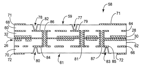
FIG 5 is a cross-sectional side view illustrating a second interconnect module
58
with a chip attach surface 59 and a board attach surface 61. As shown in FIG
5,
interconnect module 58 includes a central capacitor. structure 26 with first
and second
conductive layers 28, 30 and a first dielectric layer 32. In addition,
interconnect module
58 includes second and third dielectric layers 60, 62 on opposite sides of
central capacitor
structure 26.
A third conductive layer 64 is formed between second dielectric layer 60 and
chip
attach surface 59. A fourth conductive layer 66 is formed between third
dielectric layer
62 and board attach surface 61. First and second conductive layers 28, 30 may
form
power and ground planes, whereas third and fourth conductive layers 64, 66 may
be
patterned to form signal layers.
A fourth dielectric layer 68 is formed between third conductive layer 64 and
chip
attach surface 59, whereas a fifth dielectric layer 70 is formed between
fourth conductive
layer 66 and board attach surface 61. Finally, conductive layers 71, 72 can be
formed on
die attach surface 59 and board attach surface 61, respectively, and patterned
to define
preformed apertures for the formation of vias. Thus, the laser used to form
the vias is
applied to ablate only the dielectric material.
Conductive layers 64, 66, 71, 72 all may be formed from copper with a
thickness
in the range of approximately 5 to 14 microns and, more preferably, 12
microns. Each of
dielectric layers 60, 62, 68, 70 may have a thickness in the range of
approximately 20 to
70 microns and, more preferably, 36 microns. Thus, the distance between an
outer
surface of first conductive layer 28 and an inner surface of contact pad 71 is
less than 100
microns and, more preferably, less than or equal to approximately 88 microns.
The
various layers can be laminated together or sequentially. After conductive
layers 64, 66
are laminated to dielectric layers 60, 62, respectively, they can be patterned
to define
signal traces. Similarly, conductive layers 71, 72 can be patterned upon
lamination to
dielectric layers 68, 70, respectively.
-12-
CA 02456769 2004-02-04
WO 03/019656 PCT/US02/26756
In some embodiments, the conductive layers are "balanced" to promote
structural
uniformity and resist deformation due to thermal stresses. In particular,
conductive layers
symmetrically positioned on opposite sides of capacitor structure 26 may be
reciprocally
constructed so that each has the same type of metal foil laminated or plated
thereon and
etched into a pattern across it; the metal concentration in each layer is
approximately
equal. In this manner, the CTE of one layer and a CTE of the other layer are
substantially
equal, thereby balancing one another and minimizing warp of the interconnect
module
under thermal stress.
For I/O interconnection, interconnect module 58 includes a number of
conductive
vias, such as buried via 86, which extend through dielectric layers 60, 62 and
contact
electrodes 82, 84 at signal layers 64, 66. Electrodes 82, 84, in turn, contact
blind vias 78,
80 at chip attach surface 59 and board attach surface 61. Typically, blind
vias are formed
through only one dielectric layer and are used for routing connections between
two
adjacent conductive layers. However, blind vias can be formed that extend
through a
1 S plurality of laminated substrate layers in order to connect mufti-
conductive layers. The
conductive layers can be patterned, and any necessary blind vias to connect
adjacent
conductive layers formed, before the remaining layers are bonded to the
overall structure.
A blind via may have an entrance aperture of less than approximately 75
microns
in diameter. The range of aspect ratios for the blind vias may be in the range
of 1:1 to
5:1, inclusive. For example, a blind via may be formed having a via entrance
width of 50
microns and extending through a dielectric layer having a thickness of 50
microns.
For power and ground distribution, interconnect module 58 also includes a
number of conductive buried vias 81, 87 that contact either first conductive
plane 28 or
second conductive plane 30. Via 81 contacts an electrode 79 at signal layer 66
that, in
turn, contacts a blind via 77 formed at chip attach surface 59. Via 87
contacts an
electrode 85 at signal layer 64, which contacts a blind via 83 at board attach
surface 61.
Each buried via may have an aspect ratio of between approximately 3:1 and
25:1.
Blind vias 78, 77 receive solder balls from a chip attached to interconnect
module
58. The solder balls are heated and reflowed to form conductive bonds with
vias 78, 77,
thereby interconnecting I/O's on the chip with I/O's on the interconnect
module 58.
Likewise, blind vias 80, 83 receive solder balls to provide electrical and
mechanical
connection of the interconnect module to the board. The solder balls are
heated and
reflowed to form conductive bonds with vias 80, 83, thereby interconnecting
I/O's on the
interconnect module with I/O's on the board.
-13-
CA 02456769 2004-02-04
WO 03/019656 PCT/US02/26756
The blind and buried vias present a low inductance signal path, further
reducing
impedance in interconnect module 58. As shown in FIG. 5, via 78 contacts
conductive
layer 64, which proceeds laterally to contact buried via 86. Buried via
contacts
conductive layer 66, which proceeds laterally to contact via 80. In this
manner, portions
of the conductive layers are routed along parallel but vertically spaced
paths, with the
current or signal flowing in opposite directions.
By arranging the signals in the above manner, a mutual inductance formed by a
first signal path segment with a second adjacent signal path segment cancels a
mutual
inductance formed by the second conductive path segment with the first
conductive path
segment. This is due to the fact that current flowing through the vias flows
in one
direction in the first signal path segment and flows in an opposite direction
in an adjacent
signal path segment.
Again, in the example of FIG 5, capacitor structure 26 is extremely thin and,
at
the same time, presents a high dielectric constant. As a result, capacitor
structure 26
reduces power distribution impedance within interconnect module 58. When
combined
with the low inductance paths defined by blind and buried vias, capacitor
structure 26
yields an interconnect module capable of operating at high frequencies above
1.0
gigahertz with a power distribution impedance of less than or equal to about
0.60 ohms.
FIG. 6 is a cross-sectional side view illustrating a third interconnect module
88.
As shown in FIG. 6, third interconnect module 88 includes a central capacitor
structure
26. In addition to first and second conductive layers 28, 30 and first
dielectric layer 32,
interconnect module 88 includes a series of alternating dielectric layers 92,
93, 94, 95, 96,
98, as well as a series of alternating conductive layers 100, 102, 104, 106.
Conductive
layers 100, 102, 104, 106 may be patterned to form signal layers. Conductive
layers 28,
30 form power and ground plane layers.
Each dielectric layer 92, 93, 94, 95, 96, 98 may have a thickness in the range
of
approximately 20 to 70 microns and, more preferably, approximately 35 microns.
Thus,
each dielectric layer 92, 93, 94, 95, 96, 98 may have substantially the same
thickness and,
preferably, the same thickness tolerance. In addition, each dielectric
material 92, 93, 94,
95, 96, 98 can be formed from the same material. In some embodiments, however,
some
of the dielectric materials arranged outwardly from capacitor structure 26,
e.g., layers 92,
98, may have a higher elastic modulus than the inner dielectric layers, e.g.,
93, 94, 95, 96,
so that the flexural modulus of the interconnect module laminated substrate is
substantially maximized.
-14-
CA 02456769 2004-02-04
WO 03/019656 PCT/US02/26756
Each conductive layer 100, 102, 104, 106 may have a thickness in the range of
approximately S to 14 microns and, more preferably, approximately 12 microns.
Accordingly, the distance between an outer surface of first conductive layer
28 and an
inner surface of contact pad 112 may be less than approximately 1 SO microns.
In the
example of FIG 6, the distance is approximately 136 microns.
As shown in FIG 6, I/O interconnections are achieved by a combination of blind
and buried vias. In particular, a first blind via 108 is formed on chip attach
surface 89,
and a second blind via 110 is formed on board attach surface 91. First and
second vias
108, 110 are plated to form electrodes 112, 114, respectively. Each via 108,
110 may
receive a solder ball from a chip or board, respectively. Solder ball 116 is
illustrated in
FIG 6. Blind via 108 contacts a third blind via 118 at signal layer 106. Blind
via 110
contacts a fourth blind via 120 at signal layer 100. Blind via 118 contacts a
buried via
122 at signal layer 104, whereas blind via 120 contact the same buried via at
signal layer
102.
Power and ground plane interconnections also can be made using a combination
of blind and buried vias. As further shown in FIG 6, chip attach surface 89
includes a
blind via 121. Blind via 121 is plated to form electrode 123, and receives a
solder ball
125 associated with a chip. Blind via 121 is coupled to a second blind via 127
at signal
layer 106. In turn, blind via 127 is coupled to a buried via 129 at signal
layer 104. As in
the example of FIG 5, the arrangement of the blind and buried vias results in
cancellation
of mutual inductance in interconnect module 88, further reducing power
distribution
impedance.
Signal layer 104 contacts first conductive layer 28 of capacitor structure 26
to
interconnect solder ball 125 and the first conductive layer, which may serve
as either a
power or ground plane layer. A similar set of blind and buried vias can be
provided to
access second conductive layer 30. In addition, such vias may extend from
either chip
attach surface 89 or board attach surface 91 to distribute power and ground
potentials to
and from the chip and PWB. As in the examples of FIGS. 4 and 5, incorporation
of
capacitor structure 26 in interconnect module 88 substantially reduces power
distribution
impedance and enables faster switching frequencies.
FIG 7 is a cross-sectional side view illustrating a fourth interconnect module
130.
In the example of FIG. 7, interconnect module 130 includes two capacitor
structures 26a,
26b formed on opposite sides of a central dielectric core 132. Opposite sides
of
interconnect module 130 form a chip attach surface 131 and a board attach
surface 133.
-1 S-
CA 02456769 2004-02-04
WO 03/019656 PCT/US02/26756
Interconnect module 130 also includes an alternating arrangement of dielectric
layers 134,
135, 136, 136, 140, 142 and conductive layers 144, 146, 148, 150. Conductive
layers
144, 148 are formed on opposite sides of dielectric core 132 and may form
power and
ground planes. Conductive layers 146, 150 can be patterned to form signal
trace layers,
and are separate from conductive layers 144, 148 by dielectric layers 134,
136,
respectively.
A dielectric layer 140 is formed between conductive layer 150 and capacitor
structure 26a, whereas a dielectric layer 13 S is formed between conductive
layer 146 and
capacitor structure 26b. Dielectric layers 136, 142 are positioned adjacent
capacitor
structures 26b and 26a, respectively. Multiple vias can be formed at chip
attach surface
131 and board attach surface 133. In the example of FIG 7, a via 152 filled
with a
conductive material 154 extends through interconnect assembly 130 and
interconnects
contact pads 156, 158 on chip attach surface 131 and board attach surface 133,
respectively. Thus, via 152 may provide I/O interconnection between a chip and
a PWB.
1 S Via 160 extends from a contact pad 162 formed on chip attach surface 131
to
contact first conductive layer 28a of capacitor structure 26a. Similarly, via
164 extends
from a contact pad 166 formed on board attach layer 133 to contact first
conductive layers
28b of capacitor structure 26b. A buried via 168 extends through interconnect
module
136 to interconnect first conductive layers 28a, 28b of capacitor structures
26a, 26b.
Thus, the combination of vias 160, 164 and 168 serves to distribute power or
ground
potentials between board attach surface 133 and chip attach surface 131.
In the example of FIG 7, conductive layers 144, 146, 148, 150, 28a, 28b, 30a,
and
30b can be assigned the following functions ( in order from board attach
surface 133 to
chip attach surface 131 ):
Layer 28b: ground plane
Layer 30b: power plane
Layer 146: signal plane
Layer 144: ground plane
Layer 148: power plane
Layer 150: signal plane
Layer 30a: ground plane
Layer 28a: power plane
Conductive layers 144, 146, 148, 150 can be formed from copper and have a
thickness in
the range of approximately S to 35 microns and, more preferably, 12 microns.
Dielectric
-16-
CA 02456769 2004-02-04
WO 03/019656 PCT/US02/26756
layers 134, 135, 136, 136, 140, 142 may be formed from a variety of materials
such as
polyimide, liquid crystal polymer, fluoropolymers, epoxy resins and the like,
and have
thicknesses in the range of approximately 10 to 50 microns and, more
preferably, 20
microns. Dielectric core 132 may be formed from a variety of materials such as
BT (bis-
maleimide triazine) glass or FR4, and have a thickness in the range of 250 to
750 microns
and, more preferably, S00 microns. Conductive layers 144, 146, 148, 150 can be
patterned after they are applied to respective dielectric layers 134, 135,
136, 140 to define
signal traces or separate power and ground planes. The distance between an
outer surface
of first conductive layer 28a and an inner surface of contact pad 156 may be
less than
approximately 50 microns. In the example of FIG 7, the distance is
approximately 20
microns.
Conductive layers 28a, 28b, 30a, 30b can be pre-patterned or pre-drilled prior
to
lamination with the other layers of interconnect module 130. Capacitor
structures 26a,
26b of FIG 7 may be constructed substantially as described in the examples of
FIGS. 4-6,
I S and thereby promote reduced power distribution impedance in interconnect
module 130.
In general, one or more very thin, high dielectric constant laminates such as
capacitor
structure 26 replace the center copper plane, or "core," typically used in
existing
interconnect modules. The high dielectric constant and thin profile of
capacitor structure
26 produces a very high capacitance that reduces impedance. In addition, the
thin profile
of capacitor structure 26 in combination with reductions in the thickness of
the
interconnect module from the capacitor structure to the contact pads on the
chip attach
surface further reduces impedance.
Reducing the number of layers between capacitor structure 26 and the contact
pads and the use of thin dielectric layers less than approximately 40 microns
in thickness
achieves reduced thickness. As mentioned above, manufacture of capacitor
structure 26,
in many applications, can be readily accomplished by first patterning the
capacitor
structure laminate to form clearances for vias where desired, and then
constructing the
package substrate outward from the capacitor structure laminate by adding
additional
layers, e.g., as described in U.S. Patent Nos. 5,879,787 or 6,021,564, the
entire content of
each being incorporated herein by reference.
The increased dielectric constant and reduced thickness of capacitor structure
26
provide an increased capacitance that is a major factor in reducing power
distribution
impedance. The impact of capacitor area, dielectric thickness and dielectric
constant are
represented in the following equation:
-17-
CA 02456769 2004-02-04
WO 03/019656 PCT/US02/26756
C- so *s*A
where C is capacitance, Eo is the permittivity of free space, s is the
relative dielectric
constant, A is the area of the capacitor, and t is the thickness or distance
between the
parallel capacitor plates. Thus, in the case of an interconnect module, C is
the
capacitance formed by a pair of parallel conductive layers or planes.
The capacitance can be increased by increasing the area, decreasing the
dielectric
thickness, increasing the dielectric constant, or any combination of the
above. For the
case of on-chip capacitors, unfortunately, increasing the area leads to a
larger die,
decreasing thickness leads to increased defect density, and increasing the
dielectric
constant increases on-chip signal propagation delay.
Therefore, according the invention, the necessary capacitance is provided by a
laminated capacitor structure 26 embedded within the interconnect module. In
general, it
is desirable that the capacitor structure be placed physically as close to the
chip attach
surface as possible in an effort to minimize the series inductance to connect
to the planes,
while at the same time maximizing the capacitance of the capacitor structure
plane pair.
In addition, it is desirable that only as few circuitry layers as are
necessary be formed
between the plane pair and the chip connection, and that dielectric and
conductive layer
thicknesses be minimized.
Interconnect modules constructed according to the examples of FIGS. 4-7 may
further include structure designed to promote bonding reliability and resists
deformation
in the presence of thermal stresses. In particular, each interconnect module
is made of the
alternating laminates of conductive layers and dielectric layers, described
above, that are
selected to present on overall coefficient of thermal expansion (CTE) that
nearly matches
the CTE of the PWB.
Additionally, as described in U.S. Patent No. 5,983,974, the entire content of
which is incorporated herein by reference, a stiffener ring may be adhered to
the die
attach surface of the interconnect device. The stiffener ring defines a cavity
(or cavities)
for the integrated circuit chip and any other devices, such as capacitors,
that are attached
on the same surface to the interconnect module.
A lid may be bonded to the stiffener ring to enclose the chip within the
interconnect module package. The lid may be made of material such as copper or
may
include a preform made from a metallic material, such as aluminum, disposed in
which is
a reinforcement material, such as silicon carbide. In this case, package is
designed so that
-18-
CA 02456769 2004-02-04
WO 03/019656 PCT/US02/26756
the CTE of the stiffening ring matches the CTE of the interconnect module and
the lid.
Further, the particular adhesives used to bond the stiffening ring are chosen
to match their
CTE to that of the substrate, ring and lid. Moreover, the substrate can be
designed so that
its CTE, at least in-part, matches that of the chip, and also that of the
stiffening ring as
described in U.S. Patent No. 6,248,959, the entire content of which is
incorporated herein
by reference.
A technique for quantifying a power distribution impedance figure of merit
will
now be described. The figure of merit can be used to classify the impedance
characteristics of an interconnect module incorporating an extremely thin,
high dielectric
constant laminated capacitor structure, as described herein, in comparison to
other
interconnect modules. Other techniques for quantifying power distribution
impedance
may occur to those skilled in the art. Accordingly, the technique described
herein is not
to be considered limiting of the invention.
For any high performance mufti-layer package cross-section, there are a number
of conductive planes dedicated to either power or ground. For purposes of the
test
described herein, all of the power planes are assigned to one voltage and all
the ground
planes to another, with the intent of calculating the frequency dependent
input impedance.
Although an interconnect module may not be implemented in this manner, due to
multiple
voltage requirements, this assumption simplifies analysis of the power
distribution
impedance.
The measurement problem can be divided into two components: ground
impedance and power impedance. The power and ground impedances typically will
be
different due to the physical configuration of interconnect module 36. For
example, the
power and ground planes, e.g., first and second conductive layers 28, 30,
typically will be
positioned at different levels within interconnect module 36 and, as a result,
at different
distances from contact pads on chip attach surface 39.
First, it is assumed that the frequency is high enough that the power and
ground
planes can be treated as transmission lines. This should be a good
approximation for
operating frequencies in excess of 200 megahertz. Accordingly, transverse
electromagnetic (TEM) propagation can be assumed, which allows the
characteristic
impedance for the planes to be estimated based on the dielectric constant of
the material
in dielectric layer 32, the associated spacing to the surrounding conductive
layers 28, 30,
the frequency, and the area of interest. The calculation can be performed
according to
the following procedure:
-19-
CA 02456769 2004-02-04
WO 03/019656 PCT/US02/26756
1. Estimate the intrinsic TEM propagation delay Td as follows:
Td =~lc,
where ~r is relative dielectric constant and c is the speed of light.
2. Calculate the transmission line quarter wavelength:
l =0.25 /(f *Td),
where l is length, and f is the frequency of analysis.
3. Calculate the applicable package area:
If l > Body _ Size l 2
A = (Body _ size) z
Else
A=~*lz,
where Body Size represents the outline of the package.
4. Calculate the capacitance to adjacent planes:
a. First adjacent plane
C~ = sr * so * A l Plane _ separation, ,
where Plane separation) represents the distance between a first conductive
layer and the chip.
b. Second adjacent plane, if present
CZ = sr * so * A l Plane _ separationz
where Plane separation2 represents the distance between a second
conductive layer and the chip.
c. Total capacitance
C=C, +C2
5. Calculate the impedance of the plane
Z=l*TdlC,
wherein Z is the total impedance, C is the total capacitance produced by all
planes between the chip and the power or ground plane, and Td is the
TEM propagation delay, and l is the length calculated above.
Given the calculations above, the inductance (L) can next be calculated from
the
chip die to the connection with the first power or ground plane, by using the
equation
below:
-20-
CA 02456769 2004-02-04
WO 03/019656 PCT/US02/26756
Lvia 1 * Lwire-pair ~ t * ~O~r * COSh 1
2 2 ~c 2a
where:
d = via pair pitch,
a = via radius,
t = length of via,
,uo = permeability of free space, and
~r = relative permeability, typically 1Ø
This calculation of inductance is repeated for each subsequent power or ground
plane
layer until a connection is made between the chip die and the bottom-most
ground plane.
Repeating the power/ground impedance model calculation is a matter of joining
the transmission lines and the inductors, both as calculated above, into a
network. To
solve the network, the transmission lines are treated as frequency-independent
resistors
terminated in ground. Standard circuit analysis techniques then can be used to
solve for
the input impedance. The input impedance calculation is repeated for both the
power and
ground networks. Then, the figure of merit can be defined as the average of
the power
impedance and the ground impedance.
Set forth in Table 1 below are figures of merit for power distribution
impedance
for a number of different interconnect module constructions, including
interconnect
modules incorporating a thin, high dielectric constant capacitor structure as
described
herein and other interconnect modules without such a capacitor structure.
Table 1
indicates the impedance figure of merit over a range of operating frequencies
from 500
megahertz to 5 gigahertz.
-21-
CA 02456769 2004-02-04
WO 03/019656 PCT/US02/26756
TABLE 1
INTERCONNECT IMPEDANCE
(OHMS)
vs.
FREQUENCY
(GHz)
Type Cross-section0.5 1 GHz 2 GHz 3 GHz 4 GHz 5 GHz
GHz
7-Layer Gspgpsg 0.42 0.67 1.13 1.75 2.51 3.33
58 m
7-Layer Gspgpsg 0.31 0.51 0.88 1.36 1.93 2.53
VIP
36 m
*8-Layer gsp[gp]gsp 0.35 0.62 1.10 1.69 2.35 3.08
HiDk
(58 m)
*8-Layer gsp[gp]gsp 0.27 0.48 0.86 1.32 1.85 2.39
HiDk (36
m)
*8-Layer Xgsp[gp]gspX0.25 0.46 0.81 1.25 1.75 2.26
HiDk/VIP
(36 m)
*2-4-2 ps[gp][gp]sg0.14 0.26 0.48 0.74 1.01 1.30
Buildup
HiDk
4-2-4 Pgspgspg 0.16 0.26 0.43 0.67 0.95 1.26
Buildu
5-Layer Psgsp 0.62 0.85 1.27 2.00 2.99 4.13
(58 m)
5-Layer Psgsp 0.44 0.62 0.97 1.51 2.23 3.03
VIP
(36 pm)
*6-Layer ps[gp]sg 0.29 0.53 0.99 1.51 2.08 2.66
HiDk
I 58 m
*6-Layer ps[gp]sg 0.23 0.43 0.80 1.21 1.67 2.13
HiDk
(36 Vim)
*6-Layer Xps[gp]sgX 0.22 0.40 0.75 1.14 1.56 2.00
HiDk/VIP
36 m)
*4-Layer s[gp]s 0.23 0.44 0.87 1.30 1.75 2.20
HiDk
58 m
*4-Layer s[gp]s 0.19 0.36 0.74 1.12 1.50 1.88
HiDk
(36 m)
*4-Layer Xs[gp]sX 0.18 0.35 0.69 1.04 1.40 1.76
HiDk/V1P
36 m
Thin FilmX[gp] 0.05 0.10 0.20 0.30 0.41 0.52
on Ceramic
Substrate
In Table 1, the "Type" column refers to the type of interconnect module
construction tested. In the Type column, the designation "X-layer," e.g., "7-
layer" refers
to the number of alternating conductive layers in the interconnect module. The
-22-
CA 02456769 2004-02-04
WO 03/019656 PCT/US02/26756
designation "VIP" refers to a "via-in-pad" construction in which the
interconnect module
includes in the number of conductive layers those layers made up on contact
pads
associated with vias in the chip attach and board attach surfaces.
The designation "HiDk" refers to a construction that incorporates a thin, high
dielectric constant capacitor structure in accordance with the invention. Some
constructions are both VIP and HiDk constructions. The "Buildup" designation
refers to
a construction in which layers are built about a 500 micron dielectric. In one
case,
designated 2-4-2 Buildup HiDk, an HiDk capacitor structure is added to a
conventional
buildup core. Each HiDk construction includes a "y-x-y" designation, where the
x
indicates how many conductive layers form the HiDk capacitor structure core,
and the y
indicates how many additional conductive layers are formed on either side of
the HiDk
core.
Any thicknesses in parentheses indicate the thicknesses of the intervening
dielectric layers that separate the conductive layers in the pertinent
interconnect module.
In Table 1, all of the conductive layers are 12 micron copper. Given the
qualifications
above, the "S-layer (58 micron)" designation in the Type column indicates that
the
interconnect module under consideration has five conductive layers separated
by 58-
micron dielectric layers.
The "Cross-section" column in Table 1 indicates the arrangement of ground,
power, signal, and contact pad layers in the interconnect module. The
designation "s"
indicates a signal layer, "g" indicates a ground plane layer, "p" indicates a
power plane
layer, X indicates a via-in-pad (VIP) layer, and [gp] indicates a power-ground
plane pair
formed by a HiDk capacitor structure.
In Table 1, each "HiDk" module constructed according to the invention is
further
identified with an asterisk (*). As is apparent from Table 1, with the
exception of the S-
layer HiDk (58 micron) construction, the HiDk construction universally
produces a power
distribution impedance that is less than or equal to approximately 0.60 ohms
for operating
frequencies that are greater than or equal to approximately 1.0 gigahertz.
Given the figure of merit calculation outlined above, the 8-layer HiDk (36
micron)
construction, for example, produces a power distribution impedance of
approximately
0.48 ohms at 1.0 gigahertz. Similarly, the 8-layer HiDk/VIP construction
produces an
impedance of 0.46 ohms at 1.0 gigahertz. Even the 6-layer HiDk (58 micron)
construction produces an impedance of 0.53 ohms at 1.0 gigahertz. Notably, as
the
number of layers decreases, the impedance becomes quite low. In the case of a
4-layer
-23-
CA 02456769 2004-02-04
WO 03/019656 PCT/US02/26756
HiDk VIP construction, for example, the impedance is 0.35 ohms at 1.0
gigahertz. The 2-
4-2 Buildup HiDk construction produces, for example, an impedance of 0.26 ohms
at 1.0
gigahertz. In each case, the lower impedance promotes higher speed switching.
The last row of Table 1 represents an embodiment in which a thin film is
formed
on a ceramic substrate and combined with a capacitor structure as described
herein to
realize an interconnect module with reduced power distribution impedance.
EXAMPLE 1
Basic methods suitable for manufacturing interconnect modules with cross
sections as described herein are disclosed in U.S. Patent Nos. 5,879,787 and
6,021,564, as
mentioned above. The following example describes a representative method for
additionally producing a patterned high dielectric constant laminate, i.e., a
capacitor
structure as described with reference to FIGS. 1-7 above, for incorporation in
an
interconnect module to achieve reduced power distribution impedance. This
example
involves the use of a laminated capacitor structure comprising approximately
18 micron
copper foil on either side of a high dielectric constant material that is
approximately 8
microns in thickness.
First, the capacitor structure is formed. Copper foil substrates available
from Carl
Schenk AG, Nurenberg, Germany, are provided having a thickness of 18 microns,
an
anneal temperature of 140° centigrade and an average surface roughness
(RMS) of 8 nm.
Chemisorbed materials are removed in an oxygen/argon plasma using a device
available
from Plasma Science, Foster City, California, with a residence time of about
six minutes.
Particular debris is removed with a vacuum/ultrasonic web cleaner commercially
available from Web Systems, Inc. of Boulder, Colorado, under the trade
designation
"Ultracleaner."
Next, 6.4 grams of an epoxy commercially available from Shell Chemical
Company, of Houston, Texas, under the trade designation Epon~ 1001 F and 1.6
grams of
an epoxy commercially available from Shell Chemical Company under the trade
designation Epon~ 1050 were dissolved in 18 g of methyl ethyl ketone (MEK) and
35 g
of methyl isobutyl ketone (MBK), both of which are commercially available from
Aldrich
Chemical, Milwaukee, Wisconsin. 0.8 g of dispersant, a copolymer of polyester
and
polyamine, commercially available from ICI America, Wilmington, Delaware,
under the
trade designation "Hypermeer PS3" was added to the mixture.
-24-
CA 02456769 2004-02-04
WO 03/019656 PCT/US02/26756
47 g of barium titanate particles having an average particle size of 0.2
microns,
commercially available from Cabot Performance Materials, Boyertown,
Pennsylvania,
under the trade designation, "BT-8," which had been heated in air at 350
degrees
centigrade for 15 hours, were added slowly using a Ross laboratory
mixer/emulsifier
commercially available from Charles Ross & Sons, Hauppauge, New York, with a
rotor/stator head running at 2000 revolutions per minute (rpm). Once all of
the barium
titanate was added, the speed was increased to 6000 rpm and the barium
titanate was
dispersed for twenty minutes in a container cooled in an ice bath to prevent
heating the
blend. The resulting blend was 55% solids by weight; the volume ratio of
barium titanate
to epoxy was 55:45.
The blend was allowed to sit undisturbed overnight to allow poorly dispersed
agglomerates to settle. The blend was then filtered through a 2 micron
stainless steel
mesh filter to form a first blend. The weight percent solids of the first
blend was
measured at 53% and the volume percent loading of barium titanate in the first
blend was
measured at 53%; both measurements were made gravimetrically.
Then, 8.4 g of a 70% by weight solution of Epon~ 1001 F in MEK, 1.8 g of an
80% by weight solution of Epon~ 1050 in MEK, and 5.4 g of a 5% by weight
solution of
2,4,6-tris(dimethylaminomethyl)phenol were filtered through a 0.45 micron
filter and
then added to 236 g of the first blend to form the second blend. The blend was
made
homogeneous by stirring or letting the container roller on a ball mill
(without balls).
Final solids content of the second blend was 43% by weight. The second blend
was
deaerated using an ultrasonic bath for five minutes.
The second blend was separately coated with a microgravure coater (in a
cleanroom) onto two copper foils using a web speed of 25 feet/minute (12.7
cm/sec) and a
gravure roll speed of 40 feet/minute (20 cm/sec). Gravure rolls were chosen to
give a dry
coating thickness of from 1 to 1.5 microns. The coating was dried at 95
degrees
centigrade and then wound onto a core to form a roll.
The two blend-coated copper foils were then laminated together, in a
cleanroom,
coating side to coating side using a laminator commercially available from
Western
Magnum, El Segundo, California, with 150° centigrade rollers at 15
inches/minute (0.64
cm/sec) speed, and an air pressure to the rollers at 20 psi (140 kPa). The
laminate was
cured in air at 180 degrees centigrade for eighty minutes.
The cured laminate was tested using the 90 degree peel test described in the
IPC
Test Method Manual, IPC-TM-650, test number 2.4.9 dated October 1988,
published by
-25-
CA 02456769 2004-02-04
WO 03/019656 PCT/US02/26756
the Institute for Interconnecting and Packaging Electronic Circuits. A force
of 3.4
pounds/inch (600 N/m) was required to separate the copper foils. The cured
laminate was
also tested for capacitance by the following test method: A 2 cm by 2 cm
electrode was
etched onto one side of'the laminate using standard photolithographic and
copper etching
procedures and the capacitance was measured at 1 kilohertz using an LCR meter
available
from Hewlett Packard, Palo Alto, California, having model number 4261 A. The
measured capacitance was 6 nF/cm2 with a dissipation factor of 0.004.
Next, a sheet of the resulting capacitor laminate was cut to size according to
the
dimensions of the interconnect module. An exemplary size is 33 millimeters by
33
millimeters. The laminate was trimmed and tooling holes were formed in the
laminate
using a punch. Fiducials for photolithography alignment, which may be through
holes of
approximately 300 microns in diameter, were then lased into the punched
laminate sheet
using the tooling holes as the alignment points.
Each of the two copper foils in the laminate was then coated with type 7025
15.75
inch wide photoresist. After trimming the excess photoresist from the edges of
the
laminate, the photoresist-coated tooling holes were pierced. Then, the
Proform~ 7700
printer with auto alignment was used to image the photoresist on both foils at
standard
exposure energy. The photoresist was then developed using a sodium carbonate
solution
and standard settings. Then, the clearances in the copper foils were etched
with cupric
chloride solution and standard settings. The photoresist was stripped with
potassium
hydroxide using standard settings, except that the stripper pressure should be
lowered to
20 psi and less aggressive drying may be advisable to avoid damage to any of
the exposed
dielectric layer.
The exposed copper surfaces of the laminate were treated to increase adhesion
in
the subsequent, sequential lamination steps. Example treatments for promoting
surface
adhesion include brown or black oxide, Co-Bra~ Bond treatment, or application
of an
adhesion promoter such as aminopropyl silane.
After formation, the capacitor laminate was processed within an interconnect
module package as if it were a patterned copper sheet. In particular, the
capacitor
laminate was added within the center of other copper and dielectric layers in
an
alternating stack, and placed in a press that applied a laminate force. The
copper layers
were placed adjacent to layers, which were in a b-stage when pressed to
facilitate the
lamination process, yielding a unitary, mufti-layered structure having a HiDk
capacitor
structure core with outer dielectric and conductive layers. Multiple
laminations may be
-26-
CA 02456769 2004-02-04
WO 03/019656 PCT/US02/26756
used in order to incorporate higher circuit layer counts or various blind and
buried via
structures.
During lamination, dielectric material from the adjacent layers flowed into
and
filled the openings between the patterned conductive layers. The dielectric
layers were
made of an organic PTFE-based material. Blind and buried vias were formed in
the
interconnect module structure by drilling at different stages of assembly to
provide
interconnections between contact pads and power and ground planes. The vias
were
drilled using a laser drilling technique. In particular, a Nd:YAG pulsed laser
was used at
either the third or fourth harmonic to produce an ultraviolet beam at either
266 nm or 355
nm, as described in U.S. Patent No. 5,879,787.
To interconnect conductive layers, the blind and buried vias were plated in
stages
with a conductive material using known plating techniques such as electroless
plating
followed by electrolytic plating to define conductive paths through the
laminate.
Following plating, the outer conductive layers were patterned using standard
photolithographic techniques to form the contact pads. The contact pads were
used to
make I/O connections and power/ground plane connections. Upon assembly of the
interconnect module, including the laminated HiDk capacitor structure, a chip
was added
to the chip attach surface by reflowing an array of solder balls on the chip
to bond them to
corresponding contact pads on the chip attach surface, and the resultant
structure then
placed over a PWB for solder ball connection.
EXAMPLE 2
In another example, capacitor structure was formed with a dispersion as
described
in above-referenced U.S. application serial no. 09/902,302. In particular, a
dispersion as
indicated below in Table 2 was coated onto a copper foil using a gravure or
die coating
technique.
Table 2
Com onent Grams
Epon~ 1001 F a oxy + Epon~ 1050 a ox 16.0
9,9-bis(3-chloro-4-amino henyl) fluorine 4.0
Barium Titanate, 0.2 micron Cabot Performance 78.7
Materials)
PS3 olyester/ olyamine co of mer dis ersant (Uni 1.3
uema
I~ 5-aminobenzotriazole 0.08
-27-
CA 02456769 2004-02-04
WO 03/019656 PCT/US02/26756
Dry thicknesses of the dielectric ranged from approximately 2.0 to 5.0
microns.
The coating was dried to a tack-free surface, and then wound into rolls. Two
rolls were
laminated, coated side by side, using two heated nip rollers. A standard
photoresist
laminator was used. The laminated material was cured at 180 degrees centigrade
for 1.5
to 2.5 hours. The cured panels were patterned on one or both sides using
conventional
photoresist and etchant to produce individual capacitor structures.
EXAMPLE 3
As another example of the fabrication of a capacitor structure suitable for
use in
an interconnect module, a dispersion as described in above-referenced U.S.
application
serial no. 09/902,302 and Table 3 below was coated onto a copper foil.
Table 3
Com onent Gramsa Grams
E on~ 1001 F a oxy 20.2 16.2
E on~ 1050 epoxy S.0 4.0
9,9-bis(3-chloro-4-aminophenyl) fluorine 0 5.1
Barium Titanate, 0.2 micron (Cabot Performance100 100
Materials)
PS3 polyester/polyamine co olymer dispersant1.8 1.8
(Uniquema)
Meth 1 ethyl ketone/methyl isobutyl ketone 127 127
(4:6)
2,4,6-tris(dimethylaminomethyl)phenol 0.25 0.025
or 0
a Standard formulation using only 2,4,6-tris(dimethylaminomethyl)phenol
catalyst as the curing
agent
b 9,9-bis(3-methyl-4-aminophenyl)fluorene was also used.
The above dispersions were coated using a gravure or die coating technique.
Adhesion promoting agents may be coated onto the substrate prior to coating by
the
epoxy. Typically, a dilute solution, e.g., 0.05 to 0.15% by weight in an
alcohol such as
methanol, is applied by standard coating techniques and the substrate dried.
Dry
thicknesses of the dielectric ranged from approximately 2.0 to 5.0 microns.
The coating
was dried to a tack-free surface, and then wound into rolls. Two rolls were
subsequently
laminated, coated side by side, using two heated nip rollers in a standard
photoresist
laminator. The laminated material was cured at 180 degrees centigrade for
approximately
two hours. The cured panels were then patterned on one or both sides using
conventional
photoresist and etchant to produce individual capacitors.
-28-
CA 02456769 2004-02-04
WO 03/019656 PCT/US02/26756
EXAMPLE 4
In another example, another dispersion as described in above-referenced U.S.
application serial no. 09/902,302 and Table 3 below was coated onto a copper
foil.
Table 4
Com onent Gramsa Grams
E on~ 1001 F + E on~ 1050 a ox 16.0 16.8
9,9-bis(3-chloro-4-amino hen 1) fluorine 4.0 3.2
Amine a uivalent/e oxy a uivalent ratio 1:1 0.6:1
Barium Titanate, 0.2 micron (Cabot Performance78.7 78.7
Materials
PS3 polyester/polyamine co olymer dispersant1.8 1.8
(Uniquema)
S-aminobenzotriazole catal st 0.08 0
Initial Cure Tem erature degrees C) 180 225
Adhesion after initial cure (pounds er inch)4.4 3.4
Adhesion after six hours at 225 degrees 2.0 4.0
C (pounds per inch)
This example compares two capacitor structures with the same raw materials,
but
with changes in the ratio of fluorene compound to epoxy, presence of a
catalyst, and the
initial cure temperature. The above dispersions were coated and laminated as
in
Examples 2 and 3 above. Dry thicknesses of the dielectric ranged from
approximately 2.0
to 5.0 microns.
Various embodiments of the invention have been described. These and other
embodiments are within the scope of the following claims. For example, the
embodiments of the invention described herein may be used in combination with
any of
the additional structure or processes described in the following U.S. Patents,
the entire
content of each of which is incorporated herein by reference: U.S. Patent No.
5,888,630,
U.S. Patent No. 6,018,196, U.S. Patent No. 5,983,974, U.S. Patent No.
5,836,063, U.S.
Patent No. 5,731,047, U.S. Patent No. 5,841,075, U.S. Patent No. 5,868,950,
U.S. Patent
No. 5,888,631, U.S. Patent No. 5,900,312, U.S. Patent No. 6,011,697, U.S.
Patent No.
6,021,564, U.S. Patent No. 6,103,992, U.S. Patent No. 6,127,250, U.S. Patent
No.
6,143,401, U.S. Patent No. 6,183,592, U.S. Patent No. 6,203,891, and U.S.
Patent No.
6,248,959.
-29-