Note: Descriptions are shown in the official language in which they were submitted.
CA 02456945 2004-02-04
Doc. No. 182-Ol CA Patent
Power Management System and Method for Electronic Circuits
[001] This application claims the benefit of Provisional Application No.
60/444,639
filed February 04, 2003.
Field of the Invention
[002] The invention relates to the area of power management in electrical
circuits and
more specifically in the area of varying an amount of power provided to
individual
functional circuit blocks independence upon processing requirements of the
functional
circuit block.
Background of the Invention
[003] Circuits used in electrical devices are typically designed from
functional circuit
blocks (FCBs), where each of these blocks is designed to carry out a specific
process
within the electrical device. The FCBs are electrically linked together to
exchange data
signals therebetween. By designing electrical circuits for electrical devices
by using
FCBs, advantages are realized in the area of electrical device power
consumption. Power
consumption plays an increasingly important role in modern devices that are
being
provided with increased functionality, but must maintain sufficient battery
longevity in
order for them to be sufficiently useful between battery recharge operations.
For instance,
cellular telephones have become widespread, but in order for their continued
usefulness
they must be able to operate for longer periods of time; an issue that becomes
more
difficult when an ever increasing number of features are integrated therein,
such as, for
example, color LCD video displays, or encryption processes.
[004] It is well known to those of skill in the art to disable functional
circuit blocks
when they are not being utilized, such as United States Patent No. 6,081,135 ,
entitled
"Device and method to reduce power consumption in integrated semiconductor
devices."
This allows for electrical power stored in the battery to effectively not
power a disabled
FCB while that FCB is not being utilized, thus advantageously saving battery
power until
the previously disable FCB is required. Previously, in order to conserve
power, the entire
CA 02456945 2004-02-04
Doc. No. 182-O1 CA Patent
circuit was provided with a reduced power, which extended the battery life of
these
devices, but offered significantly reduced performance. Of course, other
options are to
also disable portion so these FCBs, leading to the same advantage that these
shut down
portions consume less power since they are disabled. Of course, the circuits
used to
monitor whether these circuits are required consume power, however these
monitor
circuit still use less electrical power than the disabled FCBs.
[005] Unfortunately, as the functional circuit blocks are enabled after being
disabled,
buffering of data therebetween must take place in order for the functional
circuit blocks
to reinstate its operation before it can accept the data. Buffering of data is
known to
consume power because logic gates in the memory circuit must be powered up,
thus
using electrical power. In addition electrical power is consumed in order to
maintain
predetermined logic states in a memory circuit. A need therefore exists to
provide a
circuit in an electrical device made from functional circuit blocks that
reduces a need for
buffering of data between the FCBs as they are being enabled.
[006] If is therefore an object of the invention to provide an electrical
device that is
made up of individual functional blocks that are individually controllable in
terms of their
power consumption, especially when these functional blocks are used in
portable
computing devices. Furthermore, it would be beneficial to reduce the amount of
power
associated with tasks involving network, transport and session layer protocols
for
computing devices.
Summary of the Invention
[007] In accordance with the invention there is provided a computing device
comprising: a plurality of functional circuit blocks (FCB)s; and, a power
controller for
reducing power provided to at least a FCB, the at least a FCB fewer than all
of the
plurality of FCBs, and of at least one of the FCBs in isolation, the power
controller for
other than disabling the functionality of the FCB having reduced power
provided thereto.
[008] In accordance with the invention there is provided a storage medium
having
stored thereon data for defining an integrated circuit component, the data
including: data
2
CA 02456945 2004-02-04
Doc. No: 182-O1 CA Patent
for a plurality of functional circuit blocks (FCB)s; and, data for a power
controller for
reducing power provided to at least a FCB, the at least a FCB fewer than all
of the
plurality of FCBs, and of at least one of the FCBs in isolation, the power
controller for
other than disabling the functionality of the FCB having reduced power
provided thereto.
[009] In accordance with the invention there is provided a method of
programming a
programmable hardware circuit (PHC) to provide a programmed PHC, the
programmed
PHC for providing circuit functionality using functional circuit blocks (FCB)s
comprising: providing first performance parameters; determining a first group
of FCB
macros that are to be used for implementing of a first set of functions within
the PHC;
optimizing the first group of FCB macros in accordance with the first
performance
parameters; and, programming the first group of optimized macros into the PHC
in order
to form a programmed PHC that operates using the first performance parameters.
[0010] In accordance with the invention there is provided a method of
programming a
programmable hardware circuit (PHC) to provide a programmed PHC, the
programmed
PHC for providing circuit functionality using functional circuit blocks (FCB)s
comprising: providing first performance parameters; providing second
performance
parameters; determining a first group of FCB macros that are to be used for
implementing
of a first set of functions within the PHC; determining a second group of FCB
macros
that are to be used for implementing of a second set of functions within the
PHC;
optimizing the first group of FCB macros in accordance with the first
performance
parameters; optimizing the second group of FCB macros in accordance with the
second
performance parameters; programming the first group and the second group of
optimized
macros into the PHC in order to form a programmed PHC that operates using one
of the
first performance parameter and the second performance parameters; and,
providing an
input port for receiving a mode of operation signal to select whether the
programmed
PHC is to operate using one of the first performance parameter and the second
performance parameters.
Brief Description of the Drawings
[0011] The invention will now be described with reference to the figures in
which:
3
CA 02456945 2004-02-04
Doc. No. 182-O 1 CA Patent
[0012] FIG. 1 illustrates power control of two functional circuit blocks using
a different
variable supply voltage provided to each of the blocks using a power control
circuit;
[0013) FIG. 2 illustrates power control of two functional circuit blocks using
a different
variable clock frequency provided to each of the blocks using a power control
circuit;
(0014) FIG. 3 illustrates power control of two functional circuit blocks using
a different
vaxiable supply voltage as well as a different variable clock frequency
provided to each of
the blocks using a power control circuit;
[0015) FIG. 4 illustrates power control of two functional circuit blocks in
dependence
upon processing requirements for each functional circuit in dependence upon
data
provided to and retrieved from a buffer memory;
[0016) FIG. 5 illustrates power control of two functional circuit blocks, in
combination
with a buffer memory for providing data to the functional circuit blocks, with
a bus
between the functional circuit blocks used to bypass storing of data back into
the buffer
memory after processing thereof in order to further reduce power;
[0017) FIG. 6 illustrates a lookup table stored within the power control
circuit fox
determining how much power to provide to each of the functional circuit
blocks;
[0018) FIG. 7 illustrates a prior art apparatus for TCP/IP termination and
security to
process all of the data for OSI protocol layers 3 to 7 using a host processor;
(0019) FIG. 8 illustrates a high-level block diagram of a system according to
the
invention for implementing TCP/IP termination over a physical link;
[0020) FIG, 9 illustrates a high-level block diagram of a system according to
the
invention;
[0021) FIG. 10 illustrates a block diagram of an alternative embodiment of the
invention that supports encryption functions;
4
CA 02456945 2004-02-04
Doc. No. 182-O1 CA Patent
[0022] FIGS. 1 la and 1 1b illustrates another embodiment of the invention, a
programmable circuit that has functional circuit blocks programmed therein in
dependence upon predetermined performance characteristics of the circuit
block; and,
[0023] FIGs. 12a and 12b illustrates another embodiment of the invention,
programming of two different types of functional circuit blocks into a
programmable
circuit, the programmable circuit having either one of the two types of
circuit blocks
enabled in dependence upon an input signal.
Detailed Description
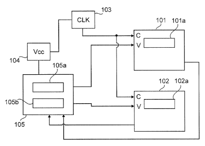
[0024] Referring to FIG. 1, a first embodiment of the invention is shown. A
clock
signal source 103 is used for providing a clock signal to a first FCB 101 and
to a second
FCB 102. A voltage source (Vcc) 104 is coupled to a power control circuit
(PCC) 105. A
first output port from the PCC 105 voltage control section l OSa is coupled to
a voltage
input port on the first FCB 101 and a second output port from the PCC 105
voltage
control section l OSa is coupled a voltage input port on the second FCB 102.
The PCC
105 in turn receives first and second data processing signals from each of the
FCBs (101
and 102), respectively, in order to use this information for varying of the
Vcc supplied to
each of the FCBs. Thus, in dependence upon the requirement for processing
capacity of
each FCB, the voltage provided thereto is varied. The more the supply voltage
is reduced
to each FCB, the lower the power consumption of that FCB. Of course, at a
certain
threshold the FCB no longer operates and thus only leakage current is observed
therein.
Thus, instead of maintaining power to an FCB that is not performing any tasks,
the PCC
disables the voltage supplied, and/or varies the clock frequency provided to
that FCB in
order to conserve power. Of course, the power supplied to each FCB is
scaleable in
dependence upon the power requirements of the FCB. Therefore, the first FCB
may fox
instance receive 40% of its normal power and the second FCB may receive 60%.
Of
course, the circuit shown in FIG 1 resides on a common substrate and power to
each of
the FCBs is individually controllable to reduce the power consumption of each
of these
FCBs in dependence upon their processing requirements as noted by their data
processing
signals.
CA 02456945 2004-02-04
Doc. No. 182-Oi CA Patent
[0025] Referring to FIG. 2, a second embodiment of the invention is shown. In
this
case, a voltage source 105 (Vcc) is used for providing a supply voltage to a
first FCB 101
and to a second FCB 102. A clock signal source 103 is coupled to a power
control circuit
(PCC) 105. A first output port from the PCC 105 clock varying section 105b is
coupled
to a clock input port on the first FCB 101 and a second output port from the
PCC 105
clock varying section 105b is coupled a clock input port on the second FCB
102. The
PCC 105 in turn receives first and second data processing signals from each of
the FCBs
( 101 and 102), respectively, in order to use this information for varying of
the clock
frequency supplied to each of the FCBs. Thus, in dependence upon the
requirement for
processing capacity of each FCB, the clock signal frequency provided thereto
is varied. It
is known to those of skill in the art that faster clock rates lead to faster
processing times,
and slower clock rates lead to slower processing times. Of course, the faster
the clock rate
that is provided to that FCB, the more power the FCB will consume. At a
certain point
the clock rate is sufficiently slow that the FCB is effectively disabled, thus
saving power.
This would be the case for an FCB that is not being utilized for processing
intensive
tasks. Of course, the clock rate supplied to each of the FCBs is dependent
upon their
processing requirements and is varied in dependence upon the first and second
data
processing signals. So, for example, the clock rate provided to the first FCB
may be 10%
of the clock rate supplied by the clock signal source 103, and the clock rate
supplied to
the second FCB may be 90% of the clock rate of the clock signal source 103.
[0026] Of course, a memory, lOla and 102a, is provided within each of the
FCBs.
Thus, when the FCBs are operating at reduced power, each of them operate in
essentially
their own environment, which means that when data is exchanged therebetween,
the
reduced clock cycles used for processing of the data preferably does not
affect the data
transfer speeds. Preferably, once the FCB b has processed its data, its clock
rate is then
synchronized with that of another FCB to facilitate transferring of data
therebetween.
[0027] Referring to FIG. 3, a third embodiment of the invention is shown. In
this case,
a voltage source 105 (Vcc) and a clock signal source 103 are both coupled to a
power
6
CA 02456945 2004-02-04
Doc. No. 182-O1 CA Patent
control circuit (PCC) 105. A first output port from the PCC 105 clock varying
section
105b is coupled to a clock input port on the f rst FCB 101 and a second output
port from
the PCC 105 clock varying section 1 OSb is coupled a clock input port on the
second FCB
102. A first output port from the PCC 105 voltage control section l OSa is
coupled to a
voltage input port on the first FCB 101 and a second output port from the PCC
105
voltage control section lOSa is coupled a voltage input port on the second FCB
102. The
PCC 105 in turn receives first and second data processing signals from each of
the FCBs
(101 and 102), respectively, in order to use this information fox varying of
both the clock
frequency and the supply voltage provided to each of the FCBs.
[0028] From the previous two embodiments, it is known that by varying both the
clock
signal frequency supplied to each FCB and by varying the supply voltage
supplied to
each FCB, the power consumption of the FCBs can be drastically reduced. Up to
a point
where the FCB does not even experience leakage current because the Vcc
supplied to the
given FCB is essentially at ground potential. Of course, an amount of voltage
and the
clock signal frequency are dependent upon the received first and second data
processing
signals.
[0029] Referring to FIG. 4, the third embodiment is shown in addition to a
buffer
memory 404. The buffer memory 404 facilitates transferring of data between the
FCBs.
An input port 404a is provided on the buffer memory for receiving of data and
an output
port is provided on the buffer memory 404b for outputting data from the buffer
memory
404. Thus, for example the system shown in FIG. 4 is used for receiving of a
TCP/IP
signal. The f rst FCB 401 is used for processing TCP/IP signals and the second
FCB 402
is used for encryption processing.
[0030] The PCC 405 monitors the status of data in the buffer memory 404 and in
dependence upon a data processing signal indicative of an amount of processed
data
output from the buffer memory output part, the PCC varies the VCC and clock
frequency
that is applied to each of the FCBs. If for example the data processing signal
indicates
that the TCP/IP signal being received is a pure TCP/IP signal, and it is not
encrypted,
then the TCP/IP FCB 401 is provided with a non reduced VCC and a non reduced
clock
7
CA 02456945 2004-02-04
Doc. No. 182-O1 CA Patent
rate by the PCC 405. The encryption FCB 102 on the other hand is provided with
at least
one of a reduced VCC and a reduced clock rate. Optionally, the VCC is reduced
to such a
point that the encryption processor is effectively provided with zero
potential, thus
effectively disabling its circuit functionality. By disabling the encryption
processor,
battery power for the device is conserved since this power is not wasted on
powering of
the encryption FCB 402. Thus, the TCP/IP FCB 401 is provided with
approximately
100% of its normal operating power and the encryption FCB 402 is effectively
provided
with 0%.
[0031] In the case of an encrypted TCP/IP signal being received on the memory
buffer
input port, the encryption FCB is enabled in order to encrypt/decrypt data
being received.
Of course, depending upon the type of encryption utilized for encoding or
decoding,
power requirements of the encryption FCB 402 will vary. Encryption processing
is
known to be processing intensive and thus providing a significant amount of
power to the
encryption FCB 402 is necessary. Thus, for example, for an intensive
encryption
throughput the clock rate provided to the encryption FCB is almost at a
maximum clock
rate, as well as the VCC provided to the encryption FCB is also at an
approximate
maximum. In this case for example, the encryption FCB 401 is provided with 90%
power
and the TCP/IP FCB 402 is provided with 10% power. If for instance 1 in 10
packets
received by the TCP/IP are encrypted then perhaps both of the FCBs receive 50%
power
each. Of course, the power provided to each is dependent upon the usage
requirements of
each FCB. The usage requirements depending upon throughput demands placed on
each
of the FCBs as indicated by the data processing signal received from the
buffer memory.
(0032] Advantageously, the power consumption of each FCB is controlled in such
a
manner so as to enable each FCB to operate with enough 'throughput that it
does not
cause a bottleneck to the system, yet while maintaining a power consumption
that is less
than that what the FCB would be using if it were not moderated.
(0033] In another example, in the case of multiband cellular telephones, there
are
typically three standards that are used in the industry. These phones termed
"tri mode"
contain necessary FCBs within that allow the phone to operate, for the most
part, all over
8
CA 02456945 2004-02-04
Doc. No. 182-O1 GA Patent
the world, in accordance with communication standards located in proximity of
the
phone. Typically, within these phones there are FCBs that are adapted for use
with each
of these standards. Unfortunately, if the power is not regulated to each of
these standard
specific FCBs, these types of phones will consumer a lot more power then their
"single
mode" counterparts. Thus, for example, if encryption is required by a given
protocol,
then an encryption FCB residing in each of the standard specific FCBs is
utilized for the
performing thereof. However, because each of the standard specific FCBs may
contain an
encryption FCB, only a single encryption FCB is necessary to carry out the
communicating encryption and decryption processes. Furthermore, each of the
standards
also requires a different bandwidth to carry out its operations. Thus, in
order to optimize
the power usage of such a tri mode phone, powering up and down of standard
specific
FCBs is not advantageous. What would be more advantageous is to provide
multiple
FCBs within the telephone that are shared by each of the communication
standards. For
example, a single encryption FCB is provided within the device for encryption
processing
for each of the standards. Not only does this save circuit layout area, but
also saves power
because only having one encryption FCB and not multiples reduce leakage
current in the
circuit. Thus, when one communication standard requires more power for
encryption
processing, then for example, the encryption FCB is provided with 70% power.
In
another example when the encryption processing is not very intensive, then the
encryption FCB is only provided with 30% power. Depending upon the bandwidth
requirements of the communication standard being utilized by the phone a the
time, the
power provided to the FCBs in the phone is managed in order to ensure that
sufficient
bandwidth is realized by the telephone, while maintaining optimum power
consumption.
In this case again, the VCC and the clock rate are varied to the encryption
FCB to ensure
that the sufficient bandwidth is realized and power consumption is minimized.
Of course,
these power levels are dependent upon the data processing signal provided to
the PCC.
[0034] Referring to FIG. 5, a fourth embodiment is shown in combination with
the
buffer memory 404. The buffer memory 404 in this case is for receiving data
from an
input port 404a located therein. A data bus 506 is provided between FCBs 401
and 402.
The data bus 506 is used to transfer of data between these FCBs without the
FCBs using
the buffer memory to exchange data therebetween. Of course, the buffer memory
404 is
9
CA 02456945 2004-02-04
Doc. No. 1$2-O 1 CA Patent
used to provide data to the FCBs, but after processing of the data by the FCB,
the FCB
forwards the data to the second FCB 402, such that intermediate storage of the
data
within the memory buffer 404 is preferably obviated.
[0035] Advantageously, by controlling the processing capabilities of each FCB
by
varying the power provided, a further power consumption advantage is realized
with the
device. When data is processed within the device by an FCB, once the FCB is
done
processing a portion of the data, the data is provided to another FCB. For
example, if a
cellular telephone is equipped with an LCD screen capable of displaying
graphics, then
three basic FCBs would be a receiver FCB, a image decoding FCB and a display
FCB. If
the receiver FCB is receiving the data at a rate that is too high for the
image decoding
FCB, then the data is typically buffered therebetween. Additionally, if the
display FCB is
slow in displaying the data on the LCD screen, then the data is buffered
between the
image decoding FCB and the display FCB. To those of skill in the art, it is
known that
buffering of data involves storing of the data in a memory circuit. Memory
circuits are
provided with input and output ports, which are controlled by number of logic
gates. The
memory storage locations also are made up of logic gates in the case of SRAM
memories, or refresh circuits when DRAM memories are employed. Thus, buffering
of
data in memory circuits is a power consumption intensive process because logic
gates are
operated, which proves to be disadvantageous when power requirements for a
device are
to be minimized. By advantageously controlling the power provided to each FCB,
resulting in varying the processing capabilities of each FCB, buffering of
data is
preferably reduced. In dependence upon a desired output bandwidth, power is
varied to
the FCB components leading up to a final FCB that provides a desired output
bandwidth,
such that power consumption is further reduced by not having to buffer data
between
FCBs.
[0036] Referring to FIG. 6, a fifth embodiment of the invention is shown. In
this case
the PCC 605 is provided with a lookup table 610 therein. The lookup table 610
contains
at least a first column 610a that has entries pertaining to the data
processing signal
received from the buffer memory 404 and at least a second column 610b that
contains
entries that are used for determining power consumption values that are
provided to each
CA 02456945 2004-02-04
Doc. No. 182-O1 CA Patent
of the FCBs (401 and 402). Thus, in dependence upon the data processing
signal,
different power consumption values are provided to the F(:Bs in order to
control the
power consumption as well as to maintain required FCB functionality for
processing of
data received from the buffer memory as well as other FCBs.
[0037) In a computer attached to a wireless network system a set of protocol
layers are
defined by the Open Systems Interconnect consortium, as is well known to those
of skill
in the art. Layers 1 and 2, the Physical Layer and Datalink Layer Protocol
respectively,
are usually closely related to the method of data transmission and would be
unique for
different protocols such as 802.11, Bluetooth, CDMA or others. These are often
implemented in hardware. The next 3 layers of the protocol called the network
(Layer 3),
transport (Layer 4), and session (Layer 5) protocols are implemented as
software in
portable devices. This allows a general-purpose device such as a portable
computer to be
used in many different network setups and support any arbitrary network
application that
is needed. The result of this implementation, however, is that the system uses
a
significant portion of the processing power of the processor as well as a
large amount of
system memory. Additionally, configuring the different software protocol and
data
handlers communicating to the host computer processor often involves a set of
complex
tasks for the user of the system.
[0038) Referring to FIG. 7, a prior art apparatus for TCP/IP termination and
security is
to process all of the data for OSI protocol layers 3 to 7 using a host
processor 701, is
shown. Packet data is transported to and from the medium through layers 1 and
2, often
implemented in hardware 702. With the advent of much higher speed networks
this
creates a processing load that is beyond the capabilities of most processors
for portable
applications and, even if the packet data were processed within the time
limits desired,
would result in increased power and thermal load of the host processor 701. In
battery-
powered mobile computing applications, it is very beneficial to reduce the
energy
consumed by the host processor 701 because this will permit more use of the
mobile
computing device between recharging or changing of a portable battery.
11
CA 02456945 2004-02-04
Doc. No. 182-O1 CA Patent
[0039] Referring to FIG. 8, an embodiment according to the invention is shown
having
host processor 701 executing applications 810, a TCP/IP offload engine (TOE)
811, and a
hardware interface 812. This embodiment of the invention converts the
processing of
Layers 3, 4, and 5 into a hardware gate level implementation, which
substantially reduces
the processor 701 load and power dissipation, permitting the use of a slower
smaller host
processor to process only Layers 6 and 7 of the protocol. Layers 6 and 7 vary
from
application to application while Layers 3, 4, and 5 are common to all TCP/IP
based data
protocols, implemented on top of a network, such as 802.1 l, W-CDMA,
Bluetooth~ and
others. For this reason Layers 5 and 7 are best implemented in software but
the
commonality of TCP/IP termination and Security processing render them amenable
to
conversion to hardware. The implementation of the zero copy protocol stack in
hardware
gate level allows for real time decoding of packet data as it is received,
reducing the need
for storage buffers.
(0040] Optionally, these functions are implemented in field programmable gate
arrays
(FPGAs), programmable array logic (PALs), or read only memory (ROMs).
Additionally,
specific protocols and data types have been indicated but the modularity of
this
embodiment of the invention does not limit it to those specific protocols or
data types.
[0041] Referring to FIG. 9, an embodiment of the invention is represented with
a high-
level block diagram. This diagram describes one possible implementation of the
invention in simple form. The interfaces to the higher levels of the protocol
are many and
varied - they may include the AMBA interface 901 promoted by ARM or other
interfaces
for other types of processors or system Input/output busses.
[0042] The TCP/IP Offload Engine (TOE) 902 is comprised of one or more finite
state
machines, processors and hardware required to implement the appropriate
functions for
termination of the data stream including packet buffering, parsing and
interpretation of
the data headers, error checking and correction, collision avoidance and
retransmission
protocols and other functions as required by the specification. The TOE 902
interacts
with the other blocks in the invention to minimize power and memory
requirements by
12
CA 02456945 2004-02-04
Doc. No. 182-O1 CA Patent
using a grab-and-go, drop-and-go philosophy to queue processing jobs onto
appropriate
resources with minimal handshaking.
[0043] The Security Offload Engine 903 is comprised of one or more finite
state
machines, processors and additional hardware used to implement the appropriate
functions for security processing under protocols such as IPv4, IPv6, IPSec,
WEP, WPA,
802.1 1i or others. The Security resources interact with the other blocks in
the device
according to the invention to minimize power and memory requirements by using
a grab-
and-go, drop-and-go philosophy to queue processing jobs onto appropriate
resources with
minimal handshaking.
[0044] The Power management block 904 manages the gating and synchronization
of
system clocks to the various blocks in the invention such that portions of the
device
which are not necessary are not consuming power by switching unnecessarily
when they
should be in the off state. It also may control the voltage levels used to
power the
invention, the slew rates of clocks and drivers within the functional logic,
the voltage bias
applied to minority carrier wells when functions are in the 'OFF' state to
minimize
leakage, and other functions meant to minimize power consumption.
[0045] The traffic management block 905 interfaces with all of the hardware
resources
in the invention to balance the loads to minimize power and memory
requirements by
using a grab-and-go, drop-and-go philosophy to queue pracessing jobs onto
appropriate
resources with minimal handshaking. This is especially important when multiple
data
streams are being terminated simultaneously a.s in a 'web-browsing' HTTP
application.
[0046] The layer 2 datalink layer interface 906 is implemented as an OMAP
interface,
or another standard implementation. In other embodiments of the invention
feature other
interfaces for other types of signal processors and system input/output busses
[0047] The TOE 902, Security Offload Engine 903, Power Management Block 904,
and Traffic Management Block 905 can recognize non-standard packets, packet
fragments or other situations not defined by the protocol and can pass packet
data in a
useful fashion to the Host processor. The Host processor software then
determines if the
13
CA 02456945 2004-02-04
Doc. No. 182-01 CA Patent
packet data represents an error condition, which is not defined by the TCP/IP,
or other
protocol, or a new packet type not recognized by the invention. In the case of
a change to
the protocol specification, obsoleting some portion of the invention hardware,
the Host
processor software can be updated to seamlessly correct such conditions when
they occur
resulting in extra Host processor load but in a continued power savings in
most normal
data transmission situations. Additionally, state machine confirmation data
and protocol
sequencing can be downloaded to the security engine and/or the TOE.
[0048] Referring to FIG. 10, a block diagram of a system 1000 according an
embodiment of the invention is shown. The system communicates with
applications
through a host interface port 1002. The system communicates with external
systems via
a wireless connection 1003. A variety of hardware circuits are disposed within
the block
diagram of the system 1000 for facilitating the communications between the
wireless
connection 1003 and the host interface 1002.
[0049] In this system 1000, a dedicated hardware circuit 1001 is used to
convert data
between different formats. The system 1000 includes a first set of dedicated
circuits for
accelerating encryption algorithms. Thus, the host processor (not shown) is
not burdened
with common encryption tasks thereby permitting the host processor to complete
other
tasks. Additionally, this system includes a second set of dedicated circuits
for handling
data having different protocols. These circuits are able to change the format
of data to
ensure that it is provided in a manner consistent with common protocols. Since
this
second set of dedicated circuits performs only one set of functions, they are
able process
data while using very little electrical energy in comparison to the amount of
energy
expended by a host processor performing the same data formatting changes.
Providing a
bypass bus 1004 advantageously allaws for received wireless data from the
wireless
connection 1003 to be provided directly to some of the FCBs prior to being
stored in a
packet buffer 1005.
[0050] In another embodiment, as illustrated in FIG. 11 a, with a method of
programming thereof outlined in FIG. 11b, hardware description language source
code, in
VHDL or Verilog for example, is used in creating of the FCBs in a programmable
14
CA 02456945 2004-02-04
Doc. No. 182-O1 CA Patent
hardware circuit (PHC). For example, within a programming system, macros that
are
used to create each FCBs are defined therein. These macros, when implemented
within
the PHC 1101, are used to define the individual FCBs 1104 a through 1104n
within the
PHC I 101 once it is programmed. Thus, once the PHC 1101 has been programmed
using
the desired macros, the PHC 1101 operates in accordance with the FCBs as
instructed by
that macro. Of course, when designing of the PHC 1101, various operating
parameters
are preferably supported in order to realize desired performance parameters
forming a
profile for the PHC 11 Ol once it is programmed. For example, prior to
programming of
the PHC 1101, the macros are optimized within the programming system in such a
manner that the resulting PHC 1101, once programmed, operates in accordance to
these
desired performance parameters. For example, one desired performance profile
parameter
is power consumption and another is processing bandwidth. Of course, typically
there is a
tradeoff between the two, where the desired performance profile far the
programmed
PHC 1101 is selected such that a desired power to performance ratio is
achieved.
[0051] If the desired performance parameters, used for optimizing of the PHC
11 O 1
prior to programming, is minimal power consumption, then once the programmed
PHC
1101 when used in an electrical circuit, it will preferably draw minimal power
thereafter.
Of course, since the programmed PHC 1101 is designed to operate using minimal
power
consumption, it does not necessarily mean that the programmed PHC 1 10l
operates using
maximum speed.
(0052] Typically, the macros for use in creating the FCBs within the PHC 1101
are
stored on a storage medium. The storage medium is thus read by the programming
system and the data for the FCBs and power controller circuit 1105 is
programmed into
the PHC 1101 to form a programmed PHC 1101. The power controller circuit 1105
is for
controlling the power provided to each of the FCBs 1104a through 1 I04n
[0053] In another example, when the programmed PHC 1101 is for use in a high
bandwidth application then speed is of prime importance. Thus, the performance
parameters provided are reflective of optimizing the PHC 1101 for maximum
processing
speed. The programming system PHC 1101 macros are chosen in accordance with
the
CA 02456945 2004-02-04
Doc. No. 182-O1 CA Patent
performance parameters and optimized in such a manner that approximately a
maximum
throughput is achievable once the PHC 1101 is programmed with those macros. Of
course, by selecting maximum bandwidth as a desired performance parameter,
that does
not necessarily imply that other desired performance parameters are met, such
as power
consumption. Typically, a tradeoff is realized.
[0054] In accordance with this embodiment, the optimization of FCBs that are
utilized
within the programmed PHC are such that the programmed PHC 1101 operates in
accordance with the desired performance parameters. Of course, once the PHC 11
O1 is
programmed, the FCBs that are used to implement functionality are not
alterable by
software. Thus, the FCB is limited to operate with the predetermined profile
selected at
the time of programming. This means that the portability of this programmed
PHC 11 O1
is limited to operate in only an environment for which it was designed.
However, by
optimizing it for different environments via the desired performance
parameters, its
applicability to various scenarios is advantageously increased.
[0055] In another embodiment of the invention, as illustrated in FIG. 12a,
with a
method of programming thereof outlined in FIG. 12b, a PHC 1201 is provided
that allows
the PHC 1201 to operate according to more than one predetermined set of
performance
parameters forming a profile. In this embodiment the programmed PHC 1201 is
provided
with an input port 1201 a that allows an end user to select which set of
desired
performance parameters are to be implemented at a predetermined time. A
profile
processor 1210 implemented in the PHC 1201 is used to determine which profile,
or
predetermined set of performance parameters, the programmed PHC 1201 is to use
to
operate. Preferably, the desired performance parameters are switchably
selectable
therebetween. In order to facilitate such a programmed PHC 1201, at least two
groups of
FCB macros are implemented in the programming system, where each set of macros
is
optimized with a specific set of desired performance parameters. Once these
optimized
macros are programmed into the PHC 1201, the PHC 1201 operates using either
the first
group or the second group in dependence upon an input signal provided to the
input port
1201 a of the PHC 1201 that is coupled to the profile processor 1210. In this
manner, the
portability of this type of programmed PHC 1201 in accordance with this
embodiment
16
--..
CA 02456945 2004-02-04
Doc. No. 182-O1 CA Patent
increases. Now, a user switchably selects whether to enable the first or the
second group
of FCBs such that for example, in a first mode of operation, when the
programmed PHC
1201 is operating in an other than power conserving mode of operation, the
programmed
PHC 1201 operates using high bandwidth throughput and thus consumes normal
amounts
of electrical power. In the second mode, when for example the programmed PHC
1201
operates using battery power, reducing power consumption is preferable, and
hence the
second group of FCBs facilitates reduced power consumption operation at an
expense of
increased throughput bandwidth. Optionally, a PROM is coupled to the
programmed
FCB, with an output port from the PROM coupled to the input port of the
profile
processor 1210 in order to provide the programmed FCB 1201 with an input
signal for
switchably selecting between the different modes of operation.
[0056] In this embodiment the storage medium has data stored therein for
profile
processing. Once the profile processor is programmed in to the PHC, the
profile
processor reads the input signal and performs selection of different operating
profiles for
the programmed PHC.
[0057] Although the invention is described herein with reference to the
specific
embodiments presented herein, one skilled in the art will readily appreciate
that a wide
variety of embodiments of the invention may be envisioned by a person of skill
in the art
of wireless network architectures without departing from the spirit and scope
of the
present invention.
17