Note: Descriptions are shown in the official language in which they were submitted.
CA 02457224 2004-02-16
WO 03/019680 PCT/US02/27623
Photonically Engineered Incandescent Emitter
STATEMENT OF GOVERNMENT INTEREST
This invention was made with Government support under contract no.
s DE-AC04-94AL85000 awarded by the U. S. Department of Energy to Sandia
Corporation. The Government has certain rights in the invention.
BACKGROUND OF THE INVENTION
The present invention relates to incandescent lamps, and more particularly
to incandescent lamps made from photonically engineered thermal emitters.
to Incandescent lamps offer very high quality lighting, are inexpensive, and
are the most popular lighting technology for residential use. They are also,
unfortunately, the least efficient (energy to useful light) lighting
technology used
commercially today. An excellent overview of incandescent lamp technology is
given in Bergman et al., Filament Lamps, GE Research and Development
~s Center, Report 98CRD027, Feb. 1998.
The lighting industry commonly uses the term luminous efficacy to
describe the efficiency of a lamp. Luminous efficacy is frequently defined as
the
luminous flux divided by the total radiant power in units of Iumens/Watt. The
luminous flux has units of lumens, and is the radiant flux weighted by the
human
2o eye response. A better description for the efficiency of a lamp is to
divide the
luminous flux by the total input power to the lighting source, so that the
electrical
performance can be factored into the comparison of lighting technologies. This
disclosure will use the latter definition for luminous efficacy, since some
lighting
approaches have inherently less efficiency in converting input electrical
power
2s into radiant power.
The luminous efficacy of a 60W incandescent lamp using a tungsten
filament is only about 15 Iumens/Watt. The luminous efficacy of the
incandescent
lamp is low because much of the light (around 90%) is emitted by the tungsten
filament in the non-visible infrared (wavelengths longer than 760 nm) portion
of
3o the spectrum. Fluorescent lamps are much more efficient than incandescent
lamps, and have luminous efficacies between 75 and 100 IumenslWatt. By
1
CA 02457224 2004-02-16
WO 03/019680 PCT/US02/27623
comparison, the theoretical maximum luminous efficacy for high-quality white
lighting using a broad spectral source is around 200 lumens/Watt.
An incandescent lamp works by heating up a tungsten filament to a
sufficiently high temperature (typically around 2800°K) that it
radiates in the
s visible portion of the electromagnetic spectrum (roughly 380 to 760 nm).
Such
high-temperature bodies are commonly referred to as "emitters" or "radiators".
The radiation from a high-temperature emitter is described by the theory of
blackbodies. An ideal blackbody emits the theoretically maximum radiation.
Real
emitters do not radiate as well as an ideal blackbody. The emissivity is the
ratio of
to the radiation from a real emitter to the radiation of an ideal blackbody,
and is
unitless with a value between 0 and 1.
The luminous efficacy of the incandescent lamp can be improved by
modifying the emissivity of the emitter. The optimum emitter for lighting
purposes
would have an emissivity of unity in the visible portion of the spectrum and
an
is emissivity of zero in the non-visible portions of the spectrum. Such an
emitter
would emit all the light in the useful visible portion of the spectrum and no
light in
the non-useful non-visible portion of the spectrum. A 2800°K emitter
with such an
optimized selective emission would have a luminous efficacy approaching 200
Iumens/Watt, or over 10X improvement compared to current incandescent lamps
2o and 2X improvement compared to current fluorescent lamps.
There remains a need for a high-temperature emitter that selectively emits
radiation in the visible portion of the spectrum, thereby enabling an
incandescent
lamp having improved luminous efficacy.
SUMMARY OF THE INVENTION
2s The present invention provides a photonically engineered incandescent
emitter, comprising a photonic crystal having a characteristic lattice
constant and
comprising an emitter material having a first dielectric constant and at least
one
other lattice material having at least one other dielectric constant and
wherein the
characteristic lattice constant, the emitter material, and the at least one
other
30 lattice material are chosen so as to create a photonic bandgap that
suppresses or
modifies thermal emission above a desired cutoff wavelength. The emitter
material can comprise a refractory non-metal or a refractory metal, such as
tungsten. The photonically engineered incandescent emitter can thereby be
CA 02457224 2004-02-16
WO 03/019680 PCT/US02/27623
tailored to selectively emit thermal radiation in the visible and near-
infrared
portions of the spectrum, enabling a more efficient incandescent lamp.
The present invention further provides a method for fabricating the
photonically engineered structure, suitable for the incandescent emitter,
comprising forming a lattice structure mold of a sacrificial material on a
substrate;
depositing a structural material into the lattice structure mold; and removing
the
sacrificial material from the lattice structure mold. Silicon integrated
circuit
technology is particularly well suited to forming the lattice structure mold
to
enable the formation of photonic crystals of refractory materials with lattice
to constants on the order of the wavelength of visible light.
BRIEF DESCRIPTION OF THE DRAWINGS
The accompanying drawings, which are incorporated in and form part of
the specification, illustrate the present invention and, together with the
description, describe the invention. In the drawings, like elements are
referred to
~s by like numbers.
Figure 1 shows the estimated luminous efficacy of an optimized
incandescent source where the emissivity is unity above and zero below a
cutoff
wavelength.
Figure 2 shows a schematic illustration of a three-dimensional (3D)
20 "Lincoln-Log" type photonic crystal structure.
Figure 3 illustrates a fabrication sequence for a four-layer Lincoln-Log type
tungsten photonic crystal.
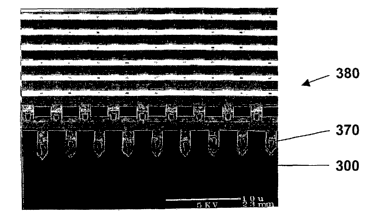
Figure 4 shows a cross-sectional scanning electron micrograph of a four-
layer tungsten photonic crystal built on a (001 ) oriented silicon substrate.
Fig. 4a
zs shows the tungsten photonic crystal prior to removal of a silica
sacrificial mold.
Fig. 4b shows the tungsten photonic crystal after removal of the silica
sacrificial
mold. The one-dimensional tungsten rod used to form the crystal has a rod
width
of 1.2 ~.m and the rod-to-rod spacing of 4.2 p.m.
Figure 5 shows the measured reflectance and transmittance spectra for
3o the light propagating along the <001 > axis of the four-layer tungsten
photonic
crystal.
Figure 6 shows the tilt-angle reflectance spectra from the four-layer
tungsten photonic crystal.
CA 02457224 2004-02-16
WO 03/019680 PCT/US02/27623
Figure 7 shows the computed transmission spectra for tungsten photonic
crystals with N = 2, 4 and 6 layers.
Figure ~ shows the spectral emissivity of the four-layer tungsten photonic
crystal having a lattice constant of 4.2 p.m.
DETAILED DESCRIPTION OF THE INVENTION
The present invention comprises a photonically engineered incandescent
emitter that is more efficient than conventional incandescent lamps and a
method
for making the same. The more efficient incandescent emitter of the present
invention is enabled by improving the emission selectivity of a high-
temperature
to emitter using photonically engineered structures. Photonically engineered
structures consist of materials with a periodic variation on the order of the
wavelength of light. The periodic variation changes the allowed optical modes
in
the medium, leading to many varied and useful properties. Some photonic
structures completely eliminate optical modes in all directions for a specific
band
is of wavelengths. These structures are said to exhibit a three-dimensional
(3D)
photonic bandgap. A description of photonic crystals and their properties is
given
by Joannopoulos et al., Photonic Crystals: Molding the Flow of Light (1995).
The thermal emission spectrum and, therefore, the emissivity can be
altered by suitable modification of the properties of photonic structures. The
use
ao of photonic structures for the control of emission of thermal radiation
from an
object is disclosed in copending U.S. Patent Application 09/441,221 to Lin and
Fleming, which is incorporated herein by reference. Modification of the
thermal
radiation from a photonic structure in the infrared portion of the spectrum
has
been described by Lin et al. in "Enhancement and suppression of thermal
2s emission by a three-dimensional photonic crystal," Phys. Rev B62, 82243
(2000).
Lin et al. fabricated a 3D "Lincoln-Log" type silicon photonic crystal with
air as the
second dielectric. The silicon photonic crystal had a lattice constant of 4.2
~.m
and a large photonic bandgap covering the infrared wavelength range from ~, =
9-
15 ~.m. When heated to 410°C, the silicon photonic crystal exhibited
significantly
3o reduced emissivity between 10 and 16 ~.m, indicative of the 3D photonic
band
gap.
CA 02457224 2004-02-16
WO 03/019680 PCT/US02/27623
Figure 1 shows the luminous efficacy for an optimized incandescent
source having an emissivity of unity above and zero below a cutoff wavelength.
The luminous efficacy is maximized by moving the cutoff wavelength as close as
possible to the long-wavelength edge of visible light (i.e., 760 nm). Luminous
s efficacies approach 200 Iumens/Watt with such an optimized emitter. Thus,
for
incandescent lighting applications in the visible portion of the spectrum, the
photonic bandgap of the photonic crystal must be closer to the long-wavelength
edge of visible light than was obtained with the silicon photonic crystal of
Lin et al.
To move the photonic bandgap closer to the long-wavelength edge of
~o visible light, the photonic crystal can have smaller dimensions and use
materials
that have greater dielectric contrast and can tolerate high temperatures
(e.g.,
2800°K). As described by Bergman et al., the most common material used
for
incandescent lamp filaments are tungsten-based materials. As a metal, tungsten
also offers the advantage of a large refractive index when used in a photonic
Is crystal. A large difference in the refractive index enhances the effect of
the
periodic variation of the refractive index on the optical modes in the
photonic
crystal, thereby producing a photonic crystal with a large photonic bandgap
wherein the emissivity is reduced.
Photonically Engineered Emitter Structures
2o The present invention discloses a 2D or 3D photonic crystal that
selectively emits at visible and near-infrared wavelengths. Various types of
photonic crystal structures that exhibit a 2D or 3D photonic bandgap known to
those in the art are suitable for the present invention. Some examples of
photonic
crystal structures and the fabrication thereof are disclosed in U.S. Patent
2s Application 09/296,702 to Fleming and Lin, which is incorporated herein by
reference.
A common type of photonic crystal exhibiting a 3D photonic bandgap that
will be used as an illustrative example in the present disclosure is the
Lincoln-Log
type of photonic crystal structure 200 shown schematically in Figure 2. The 3D
3o Lincoln-Log type structure comprises alternating layers 210, each layer 210
further comprising an evenly spaced row of parallel "logs" or rods 220 of
material
with a first dielectric constant. The spaces between the rods 220 are filled
by a
material 230 having a second dielectric constant. For simplicity as well as
for high
CA 02457224 2004-02-16
WO 03/019680 PCT/US02/27623
dielectric contrast, material 230 is often air. For a four-layer photonic
crystal 200,
the one-dimensional rods 220 have a stacking sequence that repeats itself
every
four layers with a repeat distance of c. Within each layer 210, the axes of
the rods
220 are parallel to each other with a pitch of d. Alternate layers 210 are
rotated
by 90 degrees relative to the previous layer. Between each layer 210, the rods
220 are shifted relative to each other by 0.5d. The resulting structure has a
face-
centered-tetragonal lattice symmetry of which the diamond structure is a
subset.
For the special case of c/d = 1.414, the crystal 200 can be derived from a
face-
centered-cubic unit cell with a basis of two rods.
lo Fabrication of the Photonic Crystal
Photonic crystal structures exhibiting 2D or 3D photonic bandgaps suitable
for the present invention can be fabricated by various methods known to those
skilled in the art. The vertical topology of the 3D photonic crystal structure
can be
built by repetitive deposition and etching of multiple dielectric films in a
layer-by-
~s layer method. One layer-by-layer method for fabricating the photonic
crystal is to
build up the structure directly with the structural material, as was done for
the
silicon photonic crystal of Lin et al., described above. Alternatively, the
fabrication
process can comprise forming a lattice structure mold for the structural
material in
a sacrificial material, selective deposition of the structural material into
the lattice
2o structure mold, and finally removing the sacrificial material from the
backfilled
mold to leave a photonic crystal of the structural material. The latter method
may
have advantages for structural materials that can otherwise build up large
residual stresses during a direct layer-by-layer fabrication process. This
fabrication process can be used to form photonic crystals of a wide variety of
2s structural materials that can be deposited by a conformal process,
including
metals, metal alloys, and semiconductors.
For illustrative purposes, described below and illustrated in Figures 3a - 3i
is a layer-by-layer fabrication sequence for a 3D Lincoln Log tungsten
photonic
crystal suitable for the incandescent emitter of the present invention. The
3o tungsten photonic crystal described herein has a pitch between adjacent
rods of
d = 4.2 ~,m, a rod width of w = 1.2 ~.m, and a layer thickness of 1.6 ~.m.
Photonic
crystals of other refractory metals and non-metals, such as tungsten alloys,
CA 02457224 2004-02-16
WO 03/019680 PCT/US02/27623
silicon carbide, carbon, and titanic, are also suitable for the photonically
engineered incandescent emitter of present invention.
The lattice structure mold can be formed by sequential deposition of a
cavity-forming structural material, such as polysilicon, in alternating
patterned
layers of a sacrificial mold material, such as silica (Si02). The basic layer-
by-layer
polysilicon in silica fabrication sequence is described by Lin et al. in
Nature 394,
251 (1998) and in the copending U.S. Patent Application 09/296,702 to Fleming
and Lin. The layer-by-layer fabrication method disclosed by Fleming and Lin
enables layered material composition with precise thickness, planarity, and
~o alignment control.
In Fig. 3a, a first layer 310 comprised of the sacrificial mold material,
e.g.,
silica, is deposited onto a silicon substrate 300. The thickness of silica
layer 310
is greater than the desired thickness of the first structured layer 340 of the
photonic lattice, whose thickness is typically in the range 0.02-10 ~.m,
depending
Is on the cutoff wavelength of interest. For the 3D tungsten photonic crystal
described herein, the thickness of the structured layer 340 can be 1.6 Vim,
and
the initial thickness of silica layer 310 can be approximately 2.0 ~,m.
Fig. 3b shows the first silica layer 310 patterned to form a plurality of
evenly spaced and parallel spacer bars 311 with approximately rectangular
2o cross-section. Such patterning can be accomplished using a
photolithographic
etch mask (not shown) over silica layer 310 with a plurality of openings in
the
etch mask at the locations where the material in layer 310 between the spacer
bars 311 is to be removed. An anisotropic etching process can then be used
(e.g., reactive ion etching directed normal to the surface), resulting in bars
311
2s having approximately rectangular cross-section. The etching step is
preferably
performed to etch completely down through layer 310 to the substrate 300. The
etch mask can then be stripped, resulting in the structure of Fig. 3b. In the
present example, the pitch between adjacent spacer bars 311 can be 4.2 ~.m and
the width of the spacer bars can be 3.0 ~.m.
3o In Fig. 3c, polysilicon 320 can be deposited by chemical vapor deposition
to fill in the regions between the silica spacer bars 311. Again, the
polysilicon
thickness can be greater than the desired final thickness of the first
structured
layer 340. Depositing the polysilicon 320 generally leads to a complex and non-
CA 02457224 2004-02-16
WO 03/019680 PCT/US02/27623
planar surface 321. Such a rough and uneven surface could result in a poor
quality photonic crystal, due to scattering and uncontrolled reflections at
the
growth surface. Therefore, chemical-mechanical-polishing (CMP) of the growth
surface is performed to planarize the growth surface prior to deposition of
s subsequent structural layers. CMP of the general type used in the present
invention is disclosed in U.S. Patent 5,998,298 to Fleming et al., which is
incorporated herein by reference.
As shown in Fig. 3d, a first structured layer 340 comprising a planar
pattern of silica spacer bars 311 and polysilicon rods 341 is thereby
produced.
to The polysilicon rods 341 are elongate, roughly rectangular in cross
section, and
can be 1.2 ~,m wide and 1.6 wm thick.
As shown in Fig. 3e, repeating the same basic set of growth and
processing steps, multiple structured layers 340 can be grown on top of the
substrate 300 to form the desired photonic lattice structure 350 with
polysilicon.
~s To form the Lincoln-Log structure, the orientation of the polysilicon rods
341 is
rotated 90° between each structured layer 340, and between every other
layer
the rods 341 are shifted relative to each other by half of the pitch d. The
structure
350 thereby has a face-centered-tetragonal lattice symmetry.
As shown in Fig. 3f, the polysilicon rods 341 can then be removed to form
2o the lattice structure mold 360. The polysilicon rods 341 can be removed
using a
6M, 85°C KOH etch, which has a selectivity of 100:1 (Si to Si02). Over-
etch
during the KOH process, which is desirable to ensure the removal of all the
polysilicon 341, can result in the formation of a "V" structure 361 on the
bottom of
the layer 340 contacting the silicon substrate 300. This is due to etching of
the
2s underlying silicon substrate 300 and is dependent on the substrate
crystallographic orientation. The KOH etch effectively stops when the etch-
front
encounters the slow etching (111 ) planes of the silicon substrate 300,
thereby
forming the "V" groove 361.
As shown in Fig 3g, the lattice structure mold 360 can be backfilled with a
3o structural material. A variety of deposition processes, such as chemical
vapor
deposition (CVD), electroplating, or infiltration with spin-on glasses or
nanoparticles, can be used for the backfilling of the mold 360, so long as the
sacrificial material (e.g., silica) can later be selectively removed from the
s
CA 02457224 2004-02-16
WO 03/019680 PCT/US02/27623
backfilled structural material. For example, III-V compound semiconductors, II-
VI
materials, single and mixed oxides, nitrides, oxynitrides, metals, and metal
alloys
can be deposited by CVD. A precursor conducting coating can be applied to the
lattice structure mold 360 and a wide variety of metals can be electroplated
from
s a solution to backfill the mold 360. Typical electroplated metals include
copper,
nickel, gold, iron, silver, cobalt, and chromium.
The lattice structure mold 360 can be backfilled with tungsten via CVD to
form tungsten rods 370 embedded in the silica mold material 311. A precursor
50
nm thick TiN adhesion layer (not shown) can be deposited on the mold 360 by
~o reactive ion sputtering, since the blanket CVD tungsten film does not
adhere to
silicon dioxide. Tungsten can be deposited at high pressure (e.g., 90 Torr)
from
WF6 and H2. The chemical vapor deposition of tungsten results in films of very
high purity. The tungsten film can have a resistivity of 10 g,Ohm-cm.
Backfilling of
the mold 360 with CVD tungsten 370 can result is a rough and uneven tungsten
~s growth surface 371 on the top surface of the mold 360.
As shown in Fig. 3h the top surface of the backfilled mold 360 can
planarized by CMP to remove the excess tungsten. A scanning electron
micrograph of a tungsten-backfilled, planarized mold 360 is shown in Fig. 4a.
As
shown in Fig. 4a, a keyhole 382 can be formed in the center of the more deeply
2o embedded lines of the tungsten rods 370, since the step coverage of the CVD
tungsten deposition process is not 100%. However, the film thickness is far
greater than the skin depth of tungsten for electromagnetic radiation in the
visible
and infrared.
Finally, as shown in Fig. 3i, the silica spacer bars 311 can be removed
2s from the tungsten-backfilled and planarized lattice structure mold 360 by
selective
etching with a 1:1 HF-based solution. The result is a 3D tungsten photonic
crystal
380 comprising stacked tungsten rods 370 on the silicon substrate 300. Fig. 4b
shows a scanning electron micrograph of the four-layer tungsten photonic
crystal
380 comprising the stacked tungsten rods 370 on the silicon substrate 300. The
3o tungsten photonic crystal 380 has a stacking sequence that repeats itself
every
four layers, and has a face-center-tetragonal lattice symmetry. The tungsten
rod
370 width is 1.2 ~.m, rod-to-rod spacing is 4.2 ~,m and the filling fraction
of the
9
CA 02457224 2004-02-16
WO 03/019680 PCT/US02/27623
high index tungsten is 28%. The tungsten photonic crystal 380 retains
sufficient
structural integrity to be handled readily.
This fabrication process can be extended to create almost any
interconnected photonic crystal having selective emissivity at visible or
infrared
s wavelengths. For example, current state-of-the-art silicon integrated
circuit
processing tools are capable of shrinking the minimum feature sizes to those
required for structures that have photonic bandgaps in the near infrared and
have
selective emissivity in the visible. See, e.g., "International Technology
Roadmap
for Semiconductors," 1999 Edition [retrieved on 2001-08-09]. Retrieved from
the
io Internet:<URL: http://public.itrs.net/files/1999_SIA Roadmap/Home.htm>.
Optical Properties of the Tungsten Photonic Crystal
The optical properties of the 3D tungsten photonic crystal 380 fabricated
according to the above process were characterized using a Fourier-transform
infrared measurement system for wavelengths ranging from 1.5 to 25 p.m. To
is obtain reflectance (R), a sample spectrum was taken from a 3D tungsten
photonic crystal 380 first and then normalized to a reference spectrum of a
uniform silver mirror. To find the absolute transmittance (T), a transmission
spectrum taken from a tungsten photonic crystal 380 was normalized to that of
a
bare silicon wafer. This normalization procedure was to calibrate away
extrinsic
2o effects, such as light reflection at the air-silicon interface and
absorption of the
silicon substrate 300.
Figure 5 shows the absolute reflectance spectrum 510 and transmittance
spectrum 520 of a four-layer tungsten photonic crystal 380. The dashed line
530
shows the transmittance of a 6000 uniform tungsten film for reference. Light
2s propagates along the <001 > direction of the tungsten photonic crystal 380
and is
unpolarized. The reflectance 510 exhibits oscillations at ~.< 5.5 p,m, raises
sharply
at 7~~ 6 p.m (the band edge) and finally reaches a high reflectance of 90% for
~,> 8
~.m. Correspondingly, the transmittance 520 shows distinct peaks at 7~< 5.5
pm,
decreases sharply at ~,~ 6 pm (the band edge) and then vanishes to below 1 %
for
30 ~,> 8 p.m. The simultaneous high R and low T at wavelengths greater than 8
wm
indicates the existence of a photonic band gap in the tungsten photonic
crystal.
The attenuation is ~30dB at ~,=10 pm for the four-layer tungsten photonic
crystal
to
CA 02457224 2004-02-16
WO 03/019680 PCT/US02/27623
380, or equivalently a 7.5dB attenuation per layer. The multiple oscillations
at ~,<
5.5 ~.m are attributed to photonic density-of-states oscillations in the
photonic
allowed band.
As shown in Fig. 6, tilt-angle reflection spectra were taken to determine the
s angular dependence of the photonic band gap. For tilt-angle transmission
measurements, the tungsten photonic crystal 380 was mounted on a rotational
stage and the rotational angles spanned from light incident angles from
0° to 60°,
measured from the surface normal (i.e., the <001 > direction). The crystal
orientation is tilted from the <001> to <110> axes. The light incident angle
is
to therefore systematically tilted away from G-X' toward G-L of the first
Brillouin
zone. Four tilt-angle spectra are shown in Fig. 6, for light incident angles
of 10,
30, 40, and 50°, respectively. As the light incident angle is
increased, the band
edge position moves from ~, ~ 6 ~,m for q = 10° to ~, ~ 8 ~.m for q =
50°. Both the
oscillating features at 7~ < 6 ~.m and the high reflectance at longer
wavelength
is remain for all light incident angles. Therefore, a large complete 3D
photonic band
gap exists, from 7~ ~ 8~.m to ~. > 20~,m, for the tungsten photonic crystal
380.
Figure 7 shows the theoretical transmission spectra for tungsten photonic
crystals of different number-of-layers, N=2, 4 and 6, plotted in a log-to-log
scale.
The dashed line is a reference spectrum for a uniform 6000A tungsten film. The
zo theoretical transmission spectra were calculated according to the method of
Sigalas et al. in Phys. Rev. B52, 11744 (1995). The transmittance is very low
in
the bandgap (T< 10-$ for N = 6 layers), which is consistent with the small
metallic
skin-depth (300-500 A for 1 ~.m < 7~ < 25 ~.m), and is nearly independent of
wavelength. The crystal spectrum, on the other hand, exhibits a much higher
as transmission (T~10-~) in the allowed band, suggesting that photonic
transport in
the metallic allowed band is not dominated by metallic attenuation. Moreover,
a
strong dependence on the number-of-layers of transmittance is observed in the
band gap (7~ > 8 ~.m). This number-of-layers-dependence indicates that
transmittance attenuation at ~, > 8 ~m scales with layer-thickness of the
fabricated
3o structure, but not the metallic skin depth. Hence, the observed low
transmittance
is due primarily to the photonic band gap effect. The attenuation constant in
the
band gap is extraordinarily large - about 8, 14 and 16 dB per layer at ~, =
10, 20
11
CA 02457224 2004-02-16
WO 03/019680 PCT/US02/27623
and 40 ~.m, respectively. This suggests that as few as four to six crystal
layers
are sufficient for achieving strong electromagnetic wave attenuation.
Such an extraordinarily large band gap is ideally suited for suppressing
broadband Blackbody radiation in the infrared and re-cycling radiant energy
into
visible spectrum. Figure 8 shows the spectral emissivity of the tungsten
photonic
crystal 380. The crystal 380 has a photonic bandgap (region with nearly zero
emissivity) over a large range in the far infrared (8 ~.m < ~, < 25 ~,m)
portion of the
spectrum. The very large photonic bandgap and large reduction in emissivity in
the far infrared is due to the use of metal for the photonic crystal. In the
photon
to recycling process, the photonic band gap completely frustrates infrared
thermal
emission and selectively forces the radiation into near-infrared and visible
emission. Consequently, energy is not wasted in heat generation, but rather re-
channeled into a useful emission band. The lattice constant and refractory
material of the photonic crystal can be determined by the fabrication process.
is Therefore, the emission band can be tailored to be in the visible when the
photonic crystal is heated up to an elevated temperature of >1500°C,
giving rise
to a highly efficient incandescent lamp.
It will be understood that the above description is merely illustrative of the
applications of the principles of the present invention, the scope of which is
to be
2o determined by the claims viewed in light of the specification. Other
variants and
modifications of the invention will be apparent to those of skill in the art.
12