Language selection

Search

Patent 2457499 Summary

Third-party information liability

Some of the information on this Web page has been provided by external sources. The Government of Canada is not responsible for the accuracy, reliability or currency of the information supplied by external sources. Users wishing to rely upon this information should consult directly with the source of the information. Content provided by external sources is not subject to official languages, privacy and accessibility requirements.

Claims and Abstract availability

Any discrepancies in the text and image of the Claims and Abstract are due to differing posting times. Text of the Claims and Abstract are posted:

  • At the time the application is open to public inspection;
  • At the time of issue of the patent (grant).
(12) Patent Application: (11) CA 2457499
(54) English Title: COMPENSATING FOR DIFFERENCES BETWEEN CLOCK SIGNALS
(54) French Title: COMPENSATION DE DIFFERENCES ENTRE SIGNAUX D'HORLOGE
Status: Dead
Bibliographic Data
(51) International Patent Classification (IPC):
  • H03L 7/00 (2006.01)
  • H03L 7/06 (2006.01)
  • H04L 7/00 (2006.01)
(72) Inventors :
  • DORMITZER, PAUL (United States of America)
  • ENGELSE, WILLEM (Netherlands (Kingdom of the))
  • ROBIDOUX, RAYMOND (United States of America)
(73) Owners :
  • ADC BROADBAND ACCESS SYSTEMS, INC. (United States of America)
(71) Applicants :
  • ADC BROADBAND ACCESS SYSTEMS, INC. (United States of America)
(74) Agent: ROBIC
(74) Associate agent:
(45) Issued:
(86) PCT Filing Date: 2002-08-22
(87) Open to Public Inspection: 2003-04-10
Availability of licence: N/A
(25) Language of filing: English

Patent Cooperation Treaty (PCT): Yes
(86) PCT Filing Number: PCT/US2002/026747
(87) International Publication Number: WO2003/030368
(85) National Entry: 2004-02-11

(30) Application Priority Data:
Application No. Country/Territory Date
09/935,209 United States of America 2001-08-22

Abstracts

English Abstract


A clock compensation circuit (102) is provided. The circuit comprises a clock
synchronization circuit (110) coupled to receive an input clock signal (101-
1), wherein the clock synchronization circuit generates a master clock signal
and produces a plurality of internal logic clock signals (105). The circuit
further comprises a phase comparator (120s) coupled to receive one of the
plurality of internal logic clock signals and a sample clock (PHYRET) from an
associated receiver, wherein the phase comparator generates a control signal
based on a phase comparison between the sample clock and the one of the
plurality of internal logic clock signals and a down converter channel (115s)
coupled to receive each of the plurality of internal logic clock signals and
the control signal and to pass data in phase with the sample clock using the
internal logic clock signal based on the control signal.


French Abstract

L'invention concerne un circuit de compensation d'horloge (102) qui comprend un circuit de synchronisation d'horloge (110) couplé pour recevoir un signal d'horloge d'entrée (101-1), ce circuit de synchronisation d'horloge émettant un signal d'horloge maître ainsi qu'une pluralité de signaux d'horloge logique interne (105) ; un comparateur de phases (120) couplé pour recevoir un de ces signaux d'horloge logique interne ainsi qu'une horloge d'échantillonnage (PHYRET) d'un récepteur connexe, ce comparateur de phase émettant un signal de commande sur la base d'une comparaison de phases entre l'horloge d'échantillonnage et un desdits signaux d'horloge logique interne ; et enfin, un canal de convertisseur abaisseur (115) couplé pour recevoir chacun desdits signaux d'horloge logique interne et le signal de commande, ainsi que pour transmettre les données en phase avec l'horloge d'échantillonnage en faisant intervenir le signal d'horloge logique interne sur la base du signal de commande.

Claims

Note: Claims are shown in the official language in which they were submitted.


11

What is claimed is:

1. A clock compensation circuit, comprising:
a clock synchronization circuit coupled to receive an input clock signal,
wherein the
clock synchronization circuit generates a master clock signal and produces a
plurality of
internal logic clock signals;
a phase comparator coupled to receive one of the plurality of internal logic
clock
signals and a sample clock from an associated receiver, wherein the phase
comparator
generates a control signal based on a phase comparison between the sample
clock and the one
of the plurality of internal logic clock signals; and
a down converter channel coupled to receive each of the plurality of internal
logic
clock signals and the control signal and to pass data in phase with the sample
clock using the
one of the plurality of internal logic clock signals based on the control
signal.

2. The clock compensation circuit of claim 1, wherein the clock
synchronization circuit
comprises:
a phase-locked loop coupled to receive the input clock signal and to generate
the
master clock signal; and
a clock divider coupled to receive the master clock signal and to produce the
plurality
of internal logic clock signals.

3. The clock compensation circuit of claim 1, wherein the one of the plurality
of internal
logic clock signals is matched in frequency to the sample clock.

4. The clock compensation circuit of claim 1, wherein the synchronization
circuit
receives an input clock signal on the order of 100 MHz and produces internal
logic clock
signals on the order of 20 MHz, 40 MHz, and 100 MHz.

5. The clock compensation circuit of claim 1, wherein the down converter
channel
comprises:
a first flip flop circuit coupled to receive the one of the plurality of
internal
logic clock signals and to pass a first data signal with a first phase;


12

a second flip flop circuit coupled to receive the one of the plurality of
internal
logic clock signals and to pass a second data signal 180 degrees out of phase
with the
data signal output by the first flip flop; and
a multiplexes coupled to receive the first and second data signals and the
control signal, the multiplexes selectively outputting either the first data
signal or the
second data signal based on the control signal such that the data signal
passed by the
multiplexes is in phase with the sample clock signal.

6. The clock compensation circuit of claim 1, wherein the down converter
channel
produces two selectable outputs that are 180 degrees out of phase.

7. A digital down converter, comprising:
a clock compensation circuit including:
a clock synchronization circuit coupled to receive an input clock signal,
wherein the clock synchronization circuit generates a master clock signal and
produces a plurality of internal logic clock signals;
a phase comparator coupled to receive one of the plurality of internal logic
clock signals and a sample clock from an associated receiver, wherein the
phase
comparator generates a control signal based on a phase comparison between the
sample clock and the one of the plurality of internal logic clock signals; and
a down converter channel coupled to receive each of the plurality of internal
logic clock signals and the control signal and to pass data in phase with the
sample
clock using the one of the plurality of internal logic clock signals based on
the control
signal.

8. The digital down converter of claim 7, wherein the clock synchronization
circuit
comprises:
a phase-locked loop coupled to receive the input clock signal and to generate
the
master clock signal; and
a clock divider coupled to receive the master clock signal and to produce the
plurality
of internal logic clock signals.


13

9. The digital down converter of claim 7, wherein the one of the plurality of
internal
logic clock signals is matched in frequency to the sample clock.

10. The digital down converter of claim 7, wherein the synchronization circuit
receives an
input clock signal on the order of 100 MHz and produces internal logic clock
signals on the
order of 20 MHz, 40 MHz, and 100 MHz.

11. The digital down converter of claim 7, wherein the down converter channel
comprises:
a first flip flop circuit coupled to receive the one of the plurality of
internal
logic clock signals and to pass a first data signal with a first phase;
a second flip flop circuit coupled to receive the one of the plurality of
internal
logic clock signals and to pass a second data signal 180 degrees out of phase
with the
data signal output by the first flip flop; and
a multiplexes coupled to receive the first and second data signals and the
control signal, the multiplexes selectively outputting either the first data
signal or the
second data signal based on the control signal such that the data signal
passed by the
multiplexes is in phase with the sample clock signal.

12. A clock compensation circuit, comprising:
an input for receiving an input clock signal;
a clock synchronization circuit coupled to receive the input clock signal,
wherein the
clock synchronization circuit generates a master clock signal and produces a
plurality of
internal logic clock signals;
a tapped delay line coupled to receive a first one of the plurality of
internal logic clock
signals and to generate a clock signal with a selected delay as an output
clock signal;
a phase comparator coupled to receive a second one of the plurality of
internal logic
clock signals and a sample clock from an associated receiver and to generate a
control signal
based on a phase comparison of the second one of the plurality of internal
logic clock signals
and the sample clock; and


14

a down converter channel coupled to receive the plurality of internal logic
clock
signals and the control signal and to pass data in phase with the sample clock
using the
second one of the plurality of internal logic clock signals based on the
control signal.

13. The clock compensation circuit of claim 12, wherein the clock
synchronization circuit
comprises:
a phase-locked loop coupled to receive the input clock signal and to generate
the
master clock signal; and
a clock divider coupled to receive the master clock signal and to produce the
plurality
of internal logic clock signals.

14. The clock compensation circuit of claim 12, wherein the clock divider
receives a
master clock signal on the order of 200 MHz and produces internal logic clock
signals on the
order of 20 MHz, 40 MHz, and 100 MHz.

15. The clock compensation circuit of claim 12, wherein the second one of the
plurality of
internal logic clock signals is matched in frequency to the sample clock.

16. The clock compensation circuit of claim 12, wherein the down converter
channel
comprises:
a first flip flop circuit coupled to receive the second one of the plurality
of
internal logic clock signals and to pass a first data signal with a first
phase;
a second flip flop circuit coupled to receive the second one of the plurality
of
internal logic clock signals and to pass a second data signal 180 degrees out
of phase
with the data signal output by the first flip flop; and
a multiplexer coupled to receive the first and second data signals and the
control signal, the multiplexer selectively outputting either the first data
signal or the
second data signal based on the control signal such that the data signal
passed by the
multiplexer is in phase with the sample clock signal.

17. A clock compensation circuit, comprising:
an input for receiving an input clock signal;


15

a clock synchronization circuit coupled to receive the input clock signal,
wherein the
clock synchronization circuit generates a master clock signal and produces a
plurality of
internal logic clock signals;
a phase comparator coupled to receive a first one of the plurality of internal
logic
clock signals and a sample clock from an associated receiver and to generate a
control signal
based on a phase comparison between the sample clock and the one of the
plurality of internal
logic clock signals;
a tapped delay line coupled to receive a second one of the plurality of
internal logic
clock signals and to generate a delayed clock signal for input to the
associated receiver,
wherein the delayed clock signal is synchronized with the sample clock; and
a down converter channel coupled to receive the plurality of internal logic
clock
signals and the control signal and to pass data in phase with the sample clock
using the first
one of the plurality of internal logic clock signals based on the control
signal.

18. The clock compensation circuit of claim 17, wherein the clock
synchronization circuit
comprises:
a phase-locked loop coupled to receive the input clock signal and to generate
the
master clock signal; and
a clock divider coupled to receive the master clock signal and to produce the
plurality
of internal logic clock signals.

19. The clock compensation circuit of claim 17, wherein the first one of the
plurality of
internal logic clock signals is matched in frequency to the sample clock.

20. The clock compensation circuit of claim 17, wherein the down converter
channel
comprises:
a first flip flop circuit coupled to receive the first one of the plurality of
internal logic clock signals and to pass a first data signal with a first
phase;
a second flip flop circuit coupled to receive the first one of the plurality
of
internal logic clock signals and to pass a second data signal 180 degrees out
of phase
with the data signal output by the first flip flop circuit; and


16

a multiplexes coupled to receive the first and second data signals and the
control signal, the multiplexes selectively outputting either the first data
signal or the
second data signal based on the control signal such that the data signal
passed by the
multiplexes is in phase with the sample clock signal.

21. A communications system, comprising:
a plurality of receivers, wherein each receiver is coupled to receive a data
signal and a
clock signal;
a digital down conversion circuit, including:
a clock synchronization circuit coupled to receive an input clock signal,
wherein the clock synchronization circuit generates a master clock
signal and produces a plurality of internal logic clock signals;
a plurality of phase comparators, wherein each phase comparator is coupled to
receive a first one of the plurality of internal logic clock signals and a
sample clock signal from an associated one of the plurality of receivers
and to generate a control signal based on a comparison of the phase of
the first one of the plurality of internal logic clock signals with the
sample clock signal; and
a plurality of down converter channels, wherein each of the plurality of down
converter channels is coupled to receive the plurality of internal logic
clock signals and the control signal and passes data from the data
signal in phase with the sample clock signal.

22. The communications system of claim 21, wherein the synchronization circuit
comprises:
a phase-locked loop coupled to receive the input clock signal and to generate
the
master clock signal therefrom; and
a clock divider coupled to receive the master clock signal and to produce the
plurality
of internal logic clock signals therefrom.

23. The communications system of claim 21, wherein each of the down converter
channels comprises:


17

a first flip flop circuit coupled to receive the first one of the plurality of
internal logic clock signals and to pass a first data signal with a first
phase;
a second flip flop circuit coupled to receive the first one of the plurality
of
internal logic clock signals and to pass a second data signal 180 degrees out
of phase
with the data signal output by the first flip flop circuit; and
a multiplexes coupled to receive the first and second data signals and the
control signal, the multiplexes selectively outputting either the first data
signal or the
second data signal based on the control signal such that the data signal
passed is in
phase with the sample clock signal.

24. The communications system of claim 21, further comprising a tapped delay
line
coupled to receive a second one of the plurality of internal logic clock
signals and to generate
a plurality of output clock signals with a selected delay based on the second
one of the
plurality of internal logic clock signals, wherein each of the plurality of
output clock signals is
used by the associated receiver to generate the sample clock.

25. A method of generating a timing signal, the method comprising:
receiving an input clock signal;
receiving a sample clock from an associated receiver;
generating a master clock signal from the input clock signal;
generating a plurality of internal logic clock signals from the master clock
signal;
comparing the phase of one of the plurality of internal logic clock signals to
the phase
of the received sample clock;
when the one of the plurality of internal logic clock signals is in phase with
the
received sample clock, selecting a data signal that is clocked on the rising
edge of the one of
the plurality of internal logic clock signals;
when the one of the plurality of internal logic clock signals is out of phase
with the
received sample clock, selecting the data that is clocked on the falling edge
of the one of the
plurality of internal logic clock signals; and
passing the selected data signal to the associated receiver.

26. A method of generating a timing signal, comprising:


18

receiving an input clock signal;
receiving a sample clock from an associated receiver;
generating a master clock signal from the input clock signal;
generating a plurality of internal logic clock signals from the master clock
signal;
comparing the phase of one of the plurality of internal logic clock signals to
the phase
of the received sample clock;
generating a plurality of delayed clock signals from another one of the
plurality of
logic clock signals, wherein each of the plurality of delayed clock signals is
synchronized
with the sample clock of an associated receiver;
when the one of the plurality of internal logic clock signals is in phase with
the
received sample clock, selecting a data signal that is clocked on the rising
edge of the one of
the plurality of internal logic clock signals;
when the one of the plurality of internal logic clock signals is out of phase
with the
received sample clock, selecting the data that is clocked on the falling edge
of the one of the
plurality of internal logic clock signals; and
passing the selected data signal to the associated receiver.

27. A communications system, comprising:
a plurality of analog to digital converters;
a digital down converter coupled to receive an input clock signal from one of
the
plurality of analog to digital converters, wherein the digital down converter
includes:
a clock synchronization circuit coupled to receive the input clock signal and
to
generate a master clock signal and a plurality of internal logic clock
signals;
a plurality of phase comparators, wherein each phase comparator is coupled to
receive a first one of the plurality of internal logic clock signals and a
sample clock from an
associated receiver, and wherein each phase comparator generates a control
signal based on a
phase comparison between the sample clock and the first one of the plurality
of internal logic
clock signals;
a plurality of down converter channels, wherein each down converter channel
is coupled to receive each of the plurality of internal logic clock signals
and the
control signal and to pass data in phase with the sample clock using the first
one of the
plurality of internal logic clock signals based on the control signal;


19

a plurality of receivers, each receiver associated with one of the plurality
of phase
comparators and one of the plurality of down converter channels; and
a tapped delay line coupled to a second one of the plurality of internal logic
clock
signals and to generate a clock signal with a selected delay as an output
clock signal for each
of the plurality of receivers.

28. The system of claim 27, wherein each of the plurality of down converter
channels
comprises:
a first flip flop circuit coupled to receive the first one of the plurality of
internal logic clock signals and to pass a first data signal with a first
phase;
a second flip flop circuit coupled to receive the first one of the plurality
of
internal logic clock signals and to pass a second data signal 180 degrees out
of phase
with the data signal output by the first flip flop circuit; and
a multiplexes coupled to receive the first and second data signals and the
control signal, the multiplexes selectively outputting either the first data
signal or the
second data signal based on the control signal such that the data signal
passed is in
phase with the sample clock signal.

29. The system of claim 27, wherein each of the clock synchronization circuits
comprises:
a phase-locked loop coupled to receive the input clock signal and to generate
the
master clock signal; and
a clock divider coupled to receive the master clock signal and to produce the
plurality
of internal logic clock signals.

30. A clock compensation circuit, comprising:
a clock synchronization circuit coupled to receive an input clock signal,
wherein the
clock synchronization circuit generates at least one internal logic clock
signal;
a phase comparator coupled to receive the at least one internal logic clock
signal and a
sample clock from an associated receiver, wherein the phase comparator
generates a control
signal based on a phase comparison between the sample clock and the at least
one internal
logic clock signal; and


20

a down converter channel coupled to receive the at least one internal logic
clock signal
and the control signal and to pass data in phase with the sample clock using
the internal logic
clock signal based on the control signal.

31. A clock compensation circuit, comprising:
a phase comparator coupled to receive a first clock signal and a sample clock
from an
associated receiver, wherein the phase comparator generates a control signal
based on a phase
comparison between the sample clock and the first clock signal; and
a data channel coupled to receive the first clock signal and the control
signal and to
pass data in phase with the sample clock using the first clock signal based on
the control
signal.

32. A clock compensation circuit, comprising:
a phase alignment circuit which includes:
a phase comparator coupled to receive a first clock signal and a sample clock
from an associated receiver, wherein the phase comparator generates a control
signal
based on a phase comparison between the sample clock and the first clock
signal; and
a multiplexes coupled to receive first and second data signals and the control
signal, the multiplexes selectively outputting either the first data signal or
the second
data signal based on the control signal such that the data signal passed by
the
multiplexes is in phase with the sample clock signal; and
a data channel coupled to receive the first clock signal and the control
signal and to
pass data in phase with the sample clock using the first clock signal based on
the control
signal.


Description

Note: Descriptions are shown in the official language in which they were submitted.


CA 02457499 2004-02-11
WO 03/030368 PCT/US02/26747
COMPENSATING FOR DIFFERENCES BETWEEN CLOCK SIGNALS
TECHNICAL FIELD
The present invention relates generally to the field of electronics and, in
particular,
to compensating for differences between clock signals.
BACKGROUND
Coaxial cable networks have been used to deliver high quality video
programming
to subscribers for many years. Conventionally, these networks have been
unidirectional,
broadcast networks with a limited number of channels and a limited variety of
content
provided to the subscribers. In recent years, cable companies have developed
systems to
provide bi-directional communication over their existing networks with a wider
variety of
services and content to their subscribers. For example, many cable companies
now provide
connection to the Internet through the use of cable modems.
The cable industry has developed a number of standards for delivering data
over
their networks to provide a uniform basis for the design and development of
the equipment
necessary to support these services. For example, a consortium of cable
companies
developed the Data Over Cable Service Interface Specifications (DOCSIS)
standard. The
DOCSIS standard specifies the necessary interfaces to allow for transparent,
bi-directional
transfer of Internet Protocol (IP) traffic between a cable head end and
customer equipment
over a cable or hybrid fiber/coax network.
A cable modem termination system (CMTS) is included in the head end of the
cable network for processing the upstream and downstream transmission of data.
In the
upstream, the CMTS down converts the data signals to base band or a low
intermediate
frequency, then demodulates the signals. One problem with the design of the
CMTS in many
systems is in the complexity and expense of the down conversion circuitry.
Typically, this
down conversion is accomplished with a large number of analog components that
impose
requirements in space, expense, complexity, and time to implement and tune
properly. To
address some of these problems, digital down conversion circuits can be
introduced in cable
modem termination systems (CMTSs). Unfortunately, the use of digital down
conversion
circuits introduces substantial design complication. Specifically, when a
digital down


CA 02457499 2004-02-11
WO 03/030368 PCT/US02/26747
2
conversion circuit is used, it must interact with other circuits in the CMTS,
including circuits
on other chips and from other manufacturers. Each chip or circuit may have one
or more
independent time domains with various clock signals. Differences in the time
domains
introduced by these additional clock signals complicate the timing of the
system.
For the reasons stated above, and for other reasons stated below which will
become apparent to those skilled in the art upon reading and understanding the
present
specification, there is a need in the art for techniques for compensating for
differences in
clock signals from circuits that work together in a common system.
SUMMARY
The above mentioned problems with clock domains with the implementation of
digital down conversion in communications systems and other problems are
addressed by
embodiments of the present invention and will be understood by reading and
studying the
following specification.
In one embodiment, a clock compensation circuit is provided. The circuit
comprises a clock synchronization circuit coupled to receive an input clock
signal, wherein
the clock synchronization circuit generates a master clock signal and produces
a plurality of
internal logic clock signals. The circuit further comprises a phase comparator
coupled to
receive one of the plurality of internal logic clock signals and a sample
clock from an
associated receiver, wherein the phase comparator generates a control signal
based on a phase
comparison between the sample clock and the one of the plurality of internal
logic clock
signals and a down converter channel coupled to receive each of the plurality
of internal logic
clock signals and the control signal and to pass data in phase with the sample
clock using the
internal logic clock signal based on the control signal.
In another embodiment, a clock compensation circuit is provided. The circuit
comprises an input for receiving an input clock signal, a clock
synchronization circuit coupled
to receive the input clock signal, wherein the clock synchronization circuit
generates a master
clock signal and produces a plurality of internal logic clock signals, and a
tapped delay line
coupled to receive a first one of the plurality of internal logic clock
signals and to generate a
clock signal with a selected delay as an output clock signal. In addition, the
circuit includes a
phase comparator coupled to receive a second one of the plurality of internal
logic clock


CA 02457499 2004-02-11
WO 03/030368 PCT/US02/26747
signals and a sample clock from an associated receiver and to generate a
control signal based
on a phase comparison of the second one of the plurality of internal logic
clock signals and
the sample clock, and a down converter channel coupled to receive the
plurality of internal
logic clock signals and the control signal and to pass data in phase with the
sample clock
using the second one of the plurality of internal logic clock signals based on
the control
signal.
In another embodiment, a method of generating a timing signal is provided. The
method includes receiving an input clock signal, receiving a sample clock from
an associated
receiver and generating a master clock signal from the input clock signal. The
method further
includes generating a plurality of internal logic clock signals from the
master clock signal and
comparing the phase of one of the plurality of internal logic clock signals to
the phase of the
received sample clock. When the one of the plurality of internal logic clock
signals is in
phase with the received sample clock, selecting a data signal that is clocked
on the rising edge
of the one of the plurality of internal logic clock signals. When the one of
the plurality of
internal logic clock signals is out of phase with the received sample clock,
selecting the data
that is clocked on the falling edge of the one of the plurality of internal
logic clock signals.
Further, the method includes passing the selected data signal to the
associated receiver.
In an alternate embodiment, a method of generating a timing signal is
provided.
The method includes receiving an input clock signal, receiving a sample clock
from an
associated receiver, and generating a master clock signal from the input clock
signal. The
method further includes generating a plurality of internal logic clock signals
from the master
clock signal, comparing the phase of one of the plurality of internal logic
clock signals to the
phase of the received sample clock, and generating a plurality of delayed
clock signals from
another one of the plurality of logic clock signals. Each of the plurality of
delayed clock
signals is synchronized with the sample clock of an associated receiver. When
the one of the
plurality of internal logic clock signals is in phase with the received sample
clock, selecting a
data signal that is clocked on the rising edge of the one of the plurality of
internal logic clock
signals. When the one of the plurality of internal logic clock signals is out
of phase with the
received sample clock, selecting the data that is clocked on the falling edge
of the one of the
plurality of internal logic clock signals. In addition, the method includes
passing the selected
data signal to the associated receiver.


CA 02457499 2004-02-11
WO 03/030368 PCT/US02/26747
4
BRIEF DESCRIPTION OF THE DRAWINGS
Figure 1 is a block diagram of an embodiment of a communications system
including a circuit that compensates for differences in clock signals
according to the teachings
of this invention.
Figure 2 is a flow chart of one embodiment of a method of compensating for
differences in clock signals according to the teachings of this invention.
Figure 3 is a block diagram of one embodiment of digital down converter
according to the teachings of the present invention.
DETAILED DESCRIPTION
In the following detailed description, reference is made to the accompanying
drawings that form a part hereof, and in which is shown by way of illustration
specific
illustrative embodiments in which the invention may be practiced. These
embodiments are
described in sufficient detail to enable those skilled in the art to practice
the invention, and it
is to be understood that other embodiments may be utilized and that logical,
mechanical and
electrical changes may be made without departing from the spirit and scope of
the present
invention. The following detailed description is, therefore, not to be taken
in a limiting sense.
Embodiments of the present invention provide a mechanism for compensating for
differences in clock signals between first and second circuits or chips. In
one embodiment,
the mechanism uses a tapped delay line to adjust for timing differences
between the clock
signals. Further, the mechanism compensates for phase differences between the
clock signals
by allowing data from one circuit to be clocked out to the other circuit on
either a leading
edge or a trailing edge of one of the clock signals based on a phase
difference between the
clock signals.
I. Clock Compensation
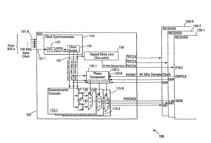
Figure 1 is a block diagram of an embodiment of a communications system,
indicated generally at 100, including a circuit that compensates for
differences in clock
signals according to the teachings of this invention. In one embodiment,
system 100 is a


CA 02457499 2004-02-11
WO 03/030368 PCT/US02/26747
portion of an upstream circuit in a cable modem termination system (CMTS).
Specifically,
system 100 includes digital down converter 102 and a plurality of receivers
150-1 to 1 SO-R.
In one embodiment, receivers 150-1 to 150-R comprise BCM 3137 Universal Burst
Receivers
commercially available from Broadcom Corporation of Irvine, CA. System 100
includes
circuitry that compensates for differences between clock signals in digital
down converter 102
and clock signals in receivers 150-1 to 150-R.
System 100 receives a plurality of input clock signals at 101-1 to 101-R.
These
clock signals are provided by R analog to digital converters. The data from
each of the digital
to analog converters is processed by a respective one of digital down
converter channels 115-
1 to 115-R as discussed in more detail below. In one embodiment, the input
clock signals are
on the order of 100 MHz clock signals.
System 100 uses one of the input clock signals at 101-1 to 101-R for
generating
internal clock signals for digital down converter 102. Digital down converter
102 includes
clock synchronization circuit 110. Clock synchronizer 110 includes phase lock
loop (PLL)
103 that is coupled to, for example, input 101-1. PLL 103 produces a master
clock with a
frequency of approximately 200 MHz that is locked to the input at 101-1. Clock
synchronization circuit 110 further includes clock divider 104. Clock divider
104 produces a
plurality of internal logic clock signals at 105. These internal logic clock
signals include, in
one embodiment, signals with frequencies on the order of 20, 40, and 100 MHz,
respectively.
In one embodiment, the internal logic clock signals have frequencies of
approximately 20.48
MHz, 40.96 MHz, and 102.4 MHz, respectively. For simplicity in description,
these signals
are referred to as having frequencies of 20, 40 and 100 MHz.
System 100 generates a clock signal for an XTALI input of receivers 150-1 to
150-
R with a selected delay based on one of the internal logic clock signals. In
one embodiment,
this clock signal is based on the 20 MHz internal logic clock signal although
other internal
logic clock signals are used in other embodiments. A Broadcom BCM 3137
Universal Burst
Receiver typically receives a signal at the XTALI input from a crystal
oscillator. From this
clock, the BCM 3137 Universal Burst Receiver typically provides a sample clock
to a digital
to analog converter at output SMPCLK. In the embodiment of Figure 1, however,
the clock
signal provided to the XTALI receivers 150-1 to 150-R is provided based on a
clock signal at


CA 02457499 2004-02-11
WO 03/030368 PCT/US02/26747
6
101-1 to 101-R of digital down converter 102 from the digital to analog
converters. This
produces at least two problems addressed by system 100.
The first problem relates to the timing of the clock signals provided at the
SMPCLK output by the receivers 150-1 to 150-R. Since there is a delay in the
path of the
receiver between the XTALI input and the SMPCLK output, the timing of the
signal applied
to the XTALI input is selectively controlled to allow the signal from SMPCLK
to align in
time with the internal logic clock signals of the digital down converter. This
delay is
prograrmned into digital down converter 102 based on experimental data and is
implemented
using tapped delay line 108. In one embodiment, tapped delay line 108 provides
selected
delay in units of 5 nanoseconds.
The second problem relates to the phase alignment of the signals in the
receivers
150-1 to 150-R and the signals in digital down converter 102. This phase
difference is
compensated for by selectively clocking data out of a down converter channel
115-1 to 115-R
based on either a leading edge or a trailing edge of the internal logic clock
signal. The
leading edge or the trailing edge is selected based on a phase comparison of
signals from a
respective one of the receivers 150-1 to 150-R and the internal logic clock
signal. A phase
comparator 120-1 to 120-R is associated with each down converter channel 115-1
to 115-R
and an associated receiver 150-1 to 150-R, respectively. A separate phase
comparison is
made for each receiver 150-1 to 150-R by its associated phase comparator 120-1
to 120-R,
respectively. A control signal is thus applied by each phase comparator 120-1
to 120-R to a
respective down converter channel 115-1 to 115-R.
Down converter channels 115-1 to 115-R include circuitry that responds to its
respective phase comparator to clock the data out on the correct phase of the
internal logic
clock signal. As each of the down converter channels is similar, only down
converter channel
115-1 is described in detail.
Down converter channel 115-1 includes first and second flip flops 130 and 132.
Each flip flop 130 and 132 receives the data for down converter channel 115-1
at its
respective D input. Flip flop 130 is clocked on the leading edge of 40 MHz
clock signal 105.
Flip flop 132 is clocked on the trailing edge of 40 MHz clock signal 105. The
output of both
flip flops 130 and 132 is provided to multiplexes 134. Multiplexes 134
receives a control
signal from its associated phase comparator 120-1. This control signal selects
either the data


CA 02457499 2004-02-11
WO 03/030368 PCT/US02/26747
7
clocked on the leading edge or the trailing edge of the internal logic clock
signal 105. This
data is phase aligned with clock signals in receiver 150-1.
The operation of system 100 is described with respect to Figure 2. This
example
is in terms of signals provided to receiver 150-1. It is understood that
signals for other
receivers are generated in a similar manner.
At block 202, digital down converter 102 receives an input clock signal. At
block
204, clock synchronization circuit 110 generates a plurality of internal clock
signals. At
block 206, phase comparator 120-1 compares the phase of a signal from receiver
150-1 with
the internal clock signal. At block 208, phase comparator 120-1 determines
whether the
signals are in phase. If the signals are in phase, phase comparator 120-1
provides a control
signal to multiplexer 134 to select the data from flip flop 130 that is
clocked on the rising
edge of the internal logic clock signal. If, however, the signals are not in
phase, phase
comparator 120-1 generates a control signal that instructs multiplexer 134 to
select the output
of flip flop 132 that is clocked on the falling edge of the internal clock
signal. At block 214,
the selected data is passed to the receiver in phase with the clock signals of
the receiver.
II. Digital Down Converter
Figure 3 is a block diagram of one embodiment of digital down converter,
indicated generally at 300, according to the teachings of the present
invention. In one
embodiment, each of digital down converters 115-1 to 115-R of Figure 1 are
constructed as
shown and described with respect to digital down converter 300 of Figure 3.
Digital down converter 300 receives an input signal at input 301.
Advantageously,
digital down converter 300 is designed to accept signals at input 301 that
comply with a
number of standards, including but not limited to, the DOCSIS standard, the
Euro-DOCSIS
standard and other appropriate standards for providing data over a cable
network. The initial
down conversion is accomplished with a mixer circuit containing a mixer 302
and a
numerically controlled oscillator 304. Mixer 302 mixes the input signal with
an output of
numerically controlled oscillator 304, which produces a down converted signal
from the
received input signal.
Digital down converter 300 further includes decimation circuit 315 that
selectively
decimates the down converted signal. Decimation circuit 315 reduces the
sampling rate of


CA 02457499 2004-02-11
WO 03/030368 PCT/US02/26747
8
the input signal down so as to reduce the burden and power consumption of the
circuitry used
to further process the signal. The decimation factor used in decimating the
down converted
signal is based on a characteristic of the input signal. In one embodiment,
the decimation
factor is based on the frequency band used for carrying data in the input
signal. It is this
ability to select the decimation factor that allows digital down converter 300
to be used with
signals compliant with any of a number of different standards.
Decimation circuit 315 prepares the input signal for further processing.
Signal
conditioning circuit 318 is coupled to decimation circuit 315 to provide the
further
processing. In one embodiment, signal conditioning circuit 318 is a low pass
filter. In
another embodiment, signal conditioning circuit 318 is a finite impulse
response low pass
filter. In other embodiments, signal conditioning circuit 318 is any other
appropriate circuit
for conditioning the signal from decimation circuit 315.
In one embodiment, decimation circuit 315 accomplishes the selective
decimation
of the input signal using two main components. These components include a
bypassable
fixed decimator 308 and a variable decimator 310. In one embodiment,
bypassable fixed
decimator 308 is a 2:1 decimator and variable decimator 310 is variable
between a 4:1 or 5:1
decimator. The decimation factors for bypassable fixed decimator 308 and
variable
decimator 310 are chosen based on the ratio of the number of samples per
second of the input
signal to a desired number of samples per second for signal conditioning
circuit 318. For
example, when the input signal is from a DOCSIS compliant system, the input
signal is
typically on the order of 100 Megasamples/second. In one embodiment, it is
desired that the
signal provided to signal conditioning circuit 318 be on the order of 20
Megasamples per
second. Thus, in this case, the bypassable fixed decimator 308 is bypassed and
the variable
decimator is set to a 5:1 decimation factor. In the case of Euro-DOCSIS, the
input signal
typically comprises 200 Megasamples/second. Thus, to provide 20
Megasamples/second to
signal conditioning circuit 318, decimation circuit 315 provides a 10:1
decimation factor.
This is accomplished by not bypassing bypassable fixed decimation circuit 308
and providing
a 5:1 decimation factor for variable decimator 310.
Signal conditioning circuit 318 is coupled to interpolator 320. Interpolator
320
increases the number of samples in the conditioned signal. In one embodiment,
interpolator


CA 02457499 2004-02-11
WO 03/030368 PCT/US02/26747
9
320 is a 2:1 interpolator and increases the number of samples in the
conditioned signal by a
factor of 2.
Control circuit 325 controls the operation of various aspects of digital down
converter 300. NCO 304 chooses the carrier frequency at which a channel is
captured from
the input signal based on control signals from control circuit 325. The Garner
frequency is
mixed with the input signals to take the desired upstream signals and cast
them down to
baseband. In one embodiment, baseband is 0 MHz. System 300 further includes a
control
circuit 325 coupled to NCO 304 and decimation circuit 315.
In one embodiment, for operation on a DOCSIS input signal received at 100
Megasamples/second, the fixed decimator 308 is selectably bypassed based on
control signals
received from control circuit 325. The input signal is then decimated by 5:1
in variable
decimator 310 to obtain a decimated signal at 20 Megasamples/second. In this
embodiment,
the 20 Megasamples/second signal is filtered via a low pass filter (signal
conditioning circuit
318) wluch rejects everything above 3.2 MHz. Once the signal has been filtered
so that it
does not have any undesirable signals or signal components the filtered signal
is interpolated
via interpolator 320.
In another embodiment, the input signal is received at 160 Megasamples/s and
decimator 308 is selected and brings the signal down to 80 Megasamples/s. The
variable
decimator 310 receives the signal and is selected for 4:1 decimation and
decimates the signal
to a 20 Megasample/second signal. In one embodiment, the combination of a 2:1
selectable
fixed decimator 308 and a variable 4:1 or 5:1 decimator 310 allows an input
sampling rate of
100, 160, or 200 Megasamples/second. The use of a 160 Megasamples/ second
signal
reduces the power usage of the digital down converter 300 and is still a high
enough
frequency to capture the entire EuroDOCSIS upstream band of 5-65 MHz.
In operation, digital down converter 300 receives an input signal and mixes
the
signal via mixer 302 with signals of NCO 304 the result is a digitally down
converted signal.
Mixer 302 and NCO 304 comprise a mixer circuit. The digitally downconverted
signal is
received by decimation circuit 315. Decimation circuit 315 decimates the
output signal of
mixer 302 based on control signals received from control circuit 325. The
received control
signals are based on the frequency of the input signal. The output of
decimation circuit 315 is
filtered in signal conditioning circuit 318 and interpolated in interpolator
320. The output of


CA 02457499 2004-02-11
WO 03/030368 PCT/US02/26747
interpolator 320 is a data stream that is selectively passed to a receiver
such as one of
receivers 150-1 to 150-R of Figure 1 through one of flip flops 130 and 132.

Representative Drawing
A single figure which represents the drawing illustrating the invention.
Administrative Status

For a clearer understanding of the status of the application/patent presented on this page, the site Disclaimer , as well as the definitions for Patent , Administrative Status , Maintenance Fee  and Payment History  should be consulted.

Administrative Status

Title Date
Forecasted Issue Date Unavailable
(86) PCT Filing Date 2002-08-22
(87) PCT Publication Date 2003-04-10
(85) National Entry 2004-02-11
Dead Application 2005-08-22

Abandonment History

Abandonment Date Reason Reinstatement Date
2004-08-23 FAILURE TO PAY APPLICATION MAINTENANCE FEE

Payment History

Fee Type Anniversary Year Due Date Amount Paid Paid Date
Application Fee $400.00 2004-02-11
Registration of a document - section 124 $100.00 2004-02-11
Owners on Record

Note: Records showing the ownership history in alphabetical order.

Current Owners on Record
ADC BROADBAND ACCESS SYSTEMS, INC.
Past Owners on Record
ADC TELCOMMUNICATIONS, INC.
DORMITZER, PAUL
ENGELSE, WILLEM
ROBIDOUX, RAYMOND
Past Owners that do not appear in the "Owners on Record" listing will appear in other documentation within the application.
Documents

To view selected files, please enter reCAPTCHA code :


To view images, click a link in the Document Description column. To download the documents, select one or more checkboxes in the first column and then click the "Download Selected in PDF format (Zip Archive)" or the "Download Selected as Single PDF" button.

List of published and non-published patent-specific documents on the CPD .

If you have any difficulty accessing content, you can call the Client Service Centre at 1-866-997-1936 or send them an e-mail at CIPO Client Service Centre.


Document
Description 
Date
(yyyy-mm-dd) 
Number of pages   Size of Image (KB) 
Abstract 2004-02-11 2 69
Drawings 2004-02-11 3 47
Claims 2004-02-11 10 470
Description 2004-02-11 10 556
Representative Drawing 2004-02-11 1 21
Cover Page 2004-04-02 1 52
PCT 2004-02-11 3 133
Assignment 2004-02-11 15 460
PCT 2004-02-12 6 289