Note: Descriptions are shown in the official language in which they were submitted.
CA 02457610 2004-02-13
INT-03-001
LOW COST ANTENNAS AND ELECTROMAGNETIC (EMF) ABSORPTION IN
ELECTRONIC CIRCUIT PACKAGES OR TRANSCEIVERS USING CONDUCTIVE
LOADED RESIN-BASED MATERIALS
This Patent Application claims priority to the following U.S. Provisional
Patent Application 60/447,825, tiled February 14, 2003, herein incorporated by
reference.
This Patent Application claims priority to U.S. Patent Application Serial
IO Number 10/075,778, filed February 14, 2002 and Patent Application Serial
Number
10/309,429, filed December 4, 2002, both of which are herein incorporated by
reference:
BACKGROUND OF THE INVENTION
(1) FIELD OF THE INVENTION
This invention relates to antennas and EMF / RFI absorbers or the like
molded of conductive loaded resin-based materials comprising micron conductive
powders, micron conductive fibers, or a combination thereof, homogenized
within a base
resin when molded.
1
CA 02457610 2004-02-13
n~~T-o3-ao 1
(2) DESCRIPTION OF THE RELATED ART
U.S. Pat. No. 4,134,120 to DeLoach et al. describes antennas formed from
fiber reinforced resin material.
U.S. Pat. No. 5,771,027 to Marks et al. describes a composite antenna
having a grid comprised of electrical conductors woven into the warp of a
resin reinforced
cloth forming one layer of a mufti-layer laminate structure of an antenna.
U.S. Pat. No. 6,249,261 B 1 to Solberg, Jr. et al. describes a direction-
finding material constructed from polymer composite materials, which are
electrically
conductive.
U.S. Pat. No 6,531,983 B1 to Hirose et aI. describes a dielectric antenna
1 S wherein a circuit pattern is fornzed of a conductive film or resin.
U.S. Pat. No. 6,320,753 Bl to Launay describes forming an antenna using
silk-screen printing of a conductive ink or a conductive resin.
U.S. Pat. No. 6,b17,976 B1 to Walden et al. teaches, without providing
details, that an antenna could be formed of conductive plastics.
2
CA 02457610 2004-02-13
INT-03-001
Patent Application Serial Number 10/075,778, filed February 14, 2002 and
Patent Application Serial Number 10/309,429, filed December 4, 2002, assigned
to the
same assignee describe low cost antennas using conductive loaded resin-based
materials.
3
CA 02457610 2004-02-13
INT-03-001
SUMMARY OF THE INVENTION
Antennas and EMF Absorbers are an essential part of electronic
communication systems that contain wireless links and electronic manufacturing
capabilities. Low cost molded antennas and EMF absorbers offer significant
advantages
for these systems not only from a fabrication standpoint, but also
characteristics related to
2D, 3D, 4D, and SD electrical characteristics, which include the physical
advantages that
can be achieved by the molding process of the actual parts and the polymer
physics within
the conductive networks formed within the molded part.
Antennas and electromagnetic absorption are essential elements in
electronic devices and wireless transceivers. Such applications as
communications and
navigation require reliable sensitive antennas and proper chip set and
electronic
component isolation either by shielding or as in with this material isolation
via EMF
absorption. Antennas and shielding (chip/component isolation) are typically
fabricated
from metals in a wide variety of configurations. Lowering the materials and or
fabrication costs combined with added performance for antennas and/or
absorbers/shielding (shielding as known when made from metals) offer
significant
advantages for many system design applications utilizing antennas or
electromagnetic
absorbers (as when made from conductive loaded resin based materials).
4
CA 02457610 2004-02-13
INT-03-001
It is a principle objective of this invention to provide a case or shell for
wireless communication devices) and/or transceivers) using next generation
moldable
antennas) and/or electro-magnetic absorber(s), which can be designed and
fabricated
from conductive loaded resin-based materials. Antennas) and absorbers) when
molded
may become part or all of the structure of the body or case of the device, or
used in
unison in all or part of the circuit board design, manufacturing and assembly
of these
devices.
It is another principle objective to provide a package for electronic circuit
devices using next generation eiectro-magnetic absorbers, which can be
designed and
fabricated from conductive loaded resin-based materials. These absorbers can
be molded
or extruded and may become part or all of the structure of the package, or
used in unison
in all or part of the design, manufacturing and assembly of these packages.
1S These objectives are achieved by molding the antenna elements and or
electronic device and or EMF chip isolation design that may be required within
the
wireless communication devices) or electronic device(s), from conductive
loaded
resin-based materials. These materials are base resins loaded with conductive
materials,
which then makes any base resin a conductor rather than an insulator. The
resins provide
the structural integrity to the rr~olded part. The micron conductive fibers,
micron
conductive powders, or a combination thereof are homogenized within the resin
during
the molding process.
5
CA 02457610 2004-02-13
INT-03-001
Any type of antenna can be produced from the conductive loaded
resin-based materials. Examples of common antennas are, dipole antennas,
monopole
antennas, planar antennas, inverted F antennas, pifa's or the like. These
antennas can be
tuned using mathematical equation multiples to achieve a desired frequency
range.
The conductive loaded resin-based materials can be molded, extruded or
the like to provide almost any desired shape or size. The molded conductive
loaded
resin-based materials can also be cut, stamped, vacuumed formed from an
injection
molded sheet or part, over-molded, laminated, milled or the like to provide
the desired
antenna or absorber shape and size. The electrical characteristics of antennas
fabricated
using conductive loaded resin-based materials, depend on the composition of
the
conductive loaded resin-based materials, of which the loading parameters can
be adjusted
to aid in achieving the desired antenna and or structural and or electrical
characteristics.
I S Virtually any antenna fabricated by conventional means such as wire, strip-
line, printed
circuit boards, or the like can be fabricated using the conductive loaded
resin-based
materials.
6
CA 02457610 2004-02-13
INT-03-001
BRIEF DESCRIPTION OF THE DRAWINGS
Fig. 1 shows a perspective view of a dipole antenna formed from a
conductive loaded resin-based material.
Fig. 2A shows a :front view of the dipole antenna of Fig. 1 showing
insulating material between the radiating antenna element and a ground plane.
Fig. 2B shows a front view of the dipole antenna of Fig. 1 showing
insulating material between both the radiating antenna element and the
counterpoise
antenna element and a ground plane.
Fig. 2C shows an amplifier inserted between the radiating antenna element
and the coaxial cable center conductor for the dipole antenna of Fig. 1.
Fig. 3 shows a segment of an antenna element formed from a conductive
loaded resin-based material showing a metal insert for connecting to
conducting cable
elements.
Fig. 4A shows a perspective view of a patch antenna comprising a
radiating antenna element and a ground plane with the coaxial cable entering
through the
ground plane.
7
CA 02457610 2004-02-13
INT-03-001
Fig. 4B shows a perspective view of a patch antenna comprising a
radiating antenna element and a ground plane with the coaxial cable entering
between the
ground plane and the radiating antenna element.
Fig. 5 shows an amplifier inserted between the radiating antenna element
and the coaxial cable center conductor for the patch antenna of Figs. 4A and
4B.
Fig. 6 shows a perspective view of a monopole antenna formed from a
conductive loaded resin-based material.
Fig. 7 shows a perspective view of a monopole antenna formed from a
conductive loaded resin-based material with an amplifier between the radiating
antenna
element and the coaxial cable center conductor.
Fig. 8A shows a. top view of an antenna having a single L shaped antenna
element formed from a conductive loaded resin-based material.
Fig. 8B shows a cross section view of the antenna element of Fig. 8A
taken along line 8B-8B' of Fig. 8A.
8
CA 02457610 2004-02-13
INT-03-001
Fig. 8C shows a cross section view of the antenna element of Fig. 8A
taken along line 8C-8C' of Fig. 8A.
Fig. 9A shows a top view of an antenna formed from a conductive loaded
S resin-based material embedded i.n an automobile bumper.
Fig. 9B shows a front view of an antenna formed from a conductive loaded
resin-based material embedded in an automobile bumper formed of an insulator
such as
rubber.
Fig. l0A shows a schematic view of an antenna formed from a conductive
loaded resin-based material embedded in the molding of a vehicle window.
Fig, l OB shows a schematic view of an antenna formed from a conductive
I5 loaded resin-based material embedded in the case of a portable electronic
device.
Fig. 1 I shows a cross section view of a conductive loaded resin-based
material comprising a powder of conductor materials.
Fig. 12A shows a cross section view of a conductive loaded resin-based
material comprising conductor fibers.
9
s
CA 02457610 2004-02-13
INT-03-001
Fig. 12B shows a cross section view of a conductive loaded resin-based
material comprising both micron conductor powder and micron conductor fibers.
Fig. 13 shows a simplified schematic view of an apparatus for forming
injection molded antenna elements.
Fig. 14 shows a simplified schematic view of an apparatus for forming
extruded antenna elements.
Fig. 15A shows a top view of fibers of conductive loaded resin-based
material woven into a conductive fabric.
Fig. 15B shows a top view of fibers of conductive loaded resin-based
material randomly webbed into a conductive fabric.
Figs. 16A, 16B, and 16C show a top view, a side view, and a cross section
view respectively of a casing for a wireless electronic communication system.
Figs. 17A and 17B show a top view and a cross section view respectively
of an integrated circuit package.
CA 02457610 2004-02-13
INT-03-001
DESCRIPTION OF THE PREFERRED EMBODIMENTS
The following embodiments are examples of antennas, ground planes, and
electromagnetic absorber isolation, fabricated using conductive loaded resin-
based
materials. In some of the examples the ground planes can be formed of either
conductive
loaded resin-based materials or in combination or unison with metals such as
circuit
boards traces or the like contained within the device as a counterpoise. The
use of
conductive loaded resin-based materials in the fabrication of antennas, ground
planes, and
electromagnetic absorber packages significantly lowers the cost of materials
and
manufacturing processes used and the ease of forming these materials into the
desired
shapes. These materials can be used to manufacture either receiving or
transmitting
antennas and any combination of antennas and/or absorbers. The antennas,
ground
planes, and EMF absorbers can be formed in infinite shapes using conventional
methods
such as injection molding, over-molding, thermo-set, protnision, extrusion,
compression
or the like of the then homogenized processed conductive loaded resin-based
materials.
The conductive loaded resin-based materials when molded typically but
not exclusively produce a desirable usable range of conductivity of between
from < 5 and
up to > 25 ohms per square. The selected materials used to build the antennas
or EMF
materials, are homogenized together using molding techniques and/or methods
such as
injection molding, over-molding, thermo-set, protrusion, extrusion,
compression, or the
like.
11
CA 02457610 2004-02-13
INT-03-001
The conductive loaded resin-based materials comprise micron conductive
powders, micron conductive fibers, or in any combination thereof. These are
homogenized together within the resin, during the molding process, yielding an
easy to
produce low cost, electrically conductive, close tolerance manufactured part
or circuit.
The micron conductive powders can be of carbons, graphite's, amines or the
like, and/or
of metal powders such as nickel, copper, silver, or plated or the like. The
use of carbons
or other forms of powders such as graphite(s) etc. can create additional low
activity level
electron exchange and, when used in combination with micron conductive fibers,
a
micron filler element within the micron conductive network of fibers)
producing further
electrical conductivity as well as acting as a lubricant for the molding
equipment. The
micron conductive fibers can be nickel plated carbon fiber, stainless steel
fiber, copper
fiber, silver fiber, or the like. The structural material is a material such
as any polymer
resin. Structural material can be, here given as examples and not as an
exhaustive list,
polymer resins produced by GE PLASTICS, Pittsfield, MA, a range of other
resins
produced by GE PLASTICS, Pittsfield, MA, a range of other resins produced by
other
manufacturers, silicones produced by GE SILICONES, Waterford, NY, or other
flexible
resin-based compounds produced by other manufacturers.
The resin-based structural material loaded with micron conductive
powders, micron conductive frbers, or in combination thereof can be molded,
using
methods such as injection molding or overmolding, or extruded to the desired
shapes.
12
CA 02457610 2004-02-13
INT-03-001
The molded conductive loaded resin-based materials can be stamped, cut or
milled as
desired to form the desired shape of the antenna elements. The composition and
directionality of the loaded materials can affect the antennas)
characteristics and can be
precisely controlled in and during the molding process. A laminated composite
could
also be in the family with random webbed micron stainless steel fibers or
other micron
conductive fibers forming a cloth like material which, when properly designed
in metal
content and shape, can be used to realize a very high performance flexible
cloth-like
antenna. Such a cloth-like antenna could be embedded in a persons clothing as
well as in
insulating materials such as rubber or plastic. The random webbed conductive
fiber can
be laminated or the like to materials such as Teflon, Polyesters, or any resin-
based
flexible or solid material polymer. When using conductive fibers as a webbed
conductor
material as part of a laminate the fibers may have diameters of between about
3 and 12
microns, typically between about 8 and 12 microns or in the range of 10
microns with
lengths) that can be seamless.
Refer now to Figs. 1-lOB for examples of antennas fabricated using
conductive loaded resin-based materials. These antennas can be either
receiving or
transmitting antennas. Fig. 1 shows a perspective drawing of a dipole antenna
with a
radiating antenna element 12 and a counterpoise antenna element 10 formed from
conductive loaded resin-based materials. The antenna comprises a radiating
antenna
element 12 and a counterpoise antenna element 10 each having a length 24 and a
rectangular cross section perpendicular to the length 24. The length 24 is
greater than
13
CA 02457610 2004-02-13
INT-03-001
three multiplied by the square root of the cross sectional area. The center
conductor 14
of a coaxial cable 50 is electrically connected to the radiating antenna
element 12 using a
solderable metal insert 15 formed in the radiating antenna element 12. The
shield 52 of
the coaxial cable 50 is connected to the counterpoise antenna element 10 using
a
solderable metal insert formed or insert molded in the counterpoise antenna
element 10.
The metal insert in the counterpoise antenna element 10 is not visible in Fig.
1 but is the
same as the metal insert 15 in the radiating antenna element 12. The length 24
is a
multiple of a quarter wavelength of the optimum frequency of detection or
transmission
of the antenna. The impedance of the antenna at resonance should be very
nearly equal to
the impedance of the coaxial cable 50 to assure maximum power transfer between
cable
and antenna.
Fig. 3 shows a detailed view of a metal insert 15 formed in a segment 11
of an antenna element. The metal insert can be copper or other metal(s). A
screw 17 can
be used in the metal insert 15 to aid in electrical connections. Soldering or
other
electrical connection methods can also be used.
Fig. 1 shows an example of a dipole antenna with the radiating antenna
element 12 placed on a layer of insulating material 22, which is placed on a
ground plane
20, and the counterpoise antenna element 10 placed directly on the ground
plane 20. The
ground plane 20 is optional and if the ground plane is not used the layer of
insulating
material 22 may not be necessary. As another option the counterpoise antenna
element
14
CA 02457610 2004-02-13
INT-03-001
can also be placed on a layer of insulating material 22, see Fig. 2A. If the
ground
plane 20 is used it can also be formed of the conductive loaded resin-based
materials.
Fig. 2A shows a front view of the dipole antenna of Fig. 1 for the example
5 of an antenna using a ground plane 20, a layer of insulating material 22
between the
radiating antenna element 12 and the ground plane 20, and the counterpoise
antenna
element 10 placed directly on the ground plane 20. Fig. 2B shows a front view
of the
dipole antenna of Fig. 1 for the example of an antenna using a ground plane 20
and a
layer of insulating material 22 between both the radiating antenna element 12
and the
10 counterpoise antenna element 10.
As shown in Fig. 2C, an amplifier 72 can be inserted between the center
conductor 14 of the coaxial cable and the radiating antenna element 12. A wire
70
connects metal insert 15 in the radiating antenna element 12 to the amplifier
72. For
receiving antennas the input of the amplifier 72 is connected to the radiating
antenna
element 12 and the output of the amplifier 72 is connected to the center
conductor 14 of
the coaxial cable 50. For transmitting antennas the output of the amplifier 72
is
connected to the radiating antenna element 12 and the input of the amplifier
72 is
connected to the center conductor 14 of the coaxial cable 50.
CA 02457610 2004-02-13
INT-03-001
In one example of this antenna the length 24 is about 1.5 inches with a
square cross section of about 0.09 square inches. This antenna had a center
frequency of
about 900 MHz.
Figs. 4A and 4B show perspective views of a patch antenna with a
radiating antenna element 40 and a ground plane 42 formed from conductive
loaded
resin-based materials. The antenna comprises a radiating antenna element 40
and a
ground plane 42 each having the shape of a rectangular plate with a thickness
44 and a
separation between the plates 46 provided by insulating standoffs 60. The
square root of
the area of the rectangular square plate forming the radiating antenna element
40 is
greater than three multiplied by the thickness 44. In one example of this
antenna wherein
the rectangular plate is a square with sides of 1.4 inches and a thickness of
0.41 inches the
patch antenna provided good performance at Global Position System, GPS,
frequencies of
about 1.5 GHz.
Fig. 4A shows an example of the patch antenna where the coaxial cable 50
enters through the ground plane 42. The coaxial cable shield 52 is connected
to the
ground plane 42 by means of a metal insert 15 in the ground plane. The coaxial
cable
center conductor 14 is connected to the radiating antenna element 40 by means
of a metal
insert 15 in the radiating antenna element 40. Fig. 4B shows an example of the
patch
antenna where the coaxial cable 50 enters between the radiating antenna
element 40 and
the ground plane 42. The coaxial cable shield 52 is connected to the ground
plane 42 by
16
CA 02457610 2004-02-13
INT-03-001
means of a metal insert 15 in the ground plane 42. The coaxial cable center
conductor 14
is connected to the radiating antenna element 40 by means of a metal insert 15
in the
radiating antenna element 40.
As shown in Fig. 5 an amplifier 72 can be inserted between the coaxial
cable center conductor 14 and the radiating antenna element 40. A wire 70
connects the
amplifier 72 to the metal insert 15 in the radiating antenna element 40. For
receiving
antennas the input of the amplifier 72 is connected to the radiating antenna
element 40
and the output of the amplifier 72 is connected to the center conductor 14 of
the coaxial
cable 50. For transmitting antennas the output of the amplifier 72 is
connected to the
radiating antenna element 40 a.nd the input of the amplifier 72 is connected
to the center
conductor 14 of the coaxial cable 50.
Fig. 6 shows an example of a monopole antenna having a radiating
antenna element 64, having a height 71, arranged perpendicular to a ground
plane 68.
The radiating antenna element 64 and the ground plane 68 are formed of
conductive
loaded resin-based materials. A layer of insulating material 66 separates the
radiating
antenna element 64 from the ground plane 68. The height 71 of the radiating
anterma
element 64 is greater than three times the square root of the cross sectional
area of the
radiating antenna element 64. An example of this antenna with a height 71 of
1.17 inches
performed well at a GPS frequency of 1.575.42 GHz.
17
CA 02457610 2004-02-13
INT-03-001
Fig. 7 shows an example of the monopole antenna described above with an
amplifier 72 inserted between the center conductor 14 of the coaxial cable 50
and the
radiating antenna element 64. For receiving antennas the input of the
amplifier 72 is
connected to the radiating antenna element 64 and the output of the amplifier
72 is
connected to the center conductor 14 of the coaxial cable 50. For transmitting
antennas
the output of the amplifier 72 is connected to the radiating antenna element
64 and the
input of the amplifier 72 is connected to the center conductor 14 of the
coaxial cable 50.
Figs. 8A, 8B, and 8C shows an example of an L shaped antenna having a
radiating antenna element 80 over a ground plane 98. The radiating antenna
element 80
and the ground plane 98 are formed of conductive loaded resin-based materials.
A layer
of insulating material 96 separates the radiating antenna element 64 from the
ground
plane 98. The radiating antenna element 80 is made up of a first leg 82 and a
second leg
84. Fig. 8A shows a top view of the antenna. Fig. 8B shows a cross section of
the first
leg 82. Fig. 8C shows a cross section of the second leg 84. Figs. 8B and 8C
show the
ground plane 98 and the layer of insulating material 96. The cross sectional
area of the
first leg 82 and the second leg 84 need not be the same. Antennas of this type
may be
typically built using overmolding technique to join the conductive resin-based
material to
the insulating material.
18
CA 02457610 2004-02-13
INT-03-001
Antennas of this type have a number of uses. Figs. 9A and 9B show a
dipole antenna, formed of conductive loaded resin-based materials, embedded in
an
automobile bumper 100, formed of insulating material. The dipole antenna has a
radiating antenna element I02 and a counterpoise antenna element 104. Fig. 9A
shows
S the top view of the bumper 100 with the embedded antenna. Fig. 9B shows the
front
view of the bumper 100 with the embedded antenna.
The antennas of this invention, formed of conductive loaded resin-based
materials, can be used for a number of additional applications. Antennas of
this type can
I 0 be embedded in the molding of a window of a vehicle, such as an automobile
or an
airplane. Fig. l0A shows a schematic view of such a window 106. The antenna
110 can
be embedded in the molding I08. Antennas of this type can be embedded in the
plastic
housing, or be part of the plastic shell itself, of portable electronic
devices such as cellular
phones, personal computers, or the like. Fig. lOB shows a schematic view of a
segment
15 112 of such a plastic housing with the antenna I 10 molded or inserted in
the housing I 12.
The conductive loaded resin-based material typically comprises a powder
of conductor particles, fibers of a conductor material, or a combination
thereof in a base
resin host. Fig. 11 shows cross section view of an example of conductor loaded
resin-
20 based material 212 having powder of conductor particles 202 in a base resin
host 204.
Fig. 12A shows a cross section view of an example of conductor loaded resin-
based
material 212 having conductor fibers 210 in a base resin host 204. Fig. 12B
shows a
19
CA 02457610 2004-02-13
INT-03=001
cross section view of an example of conductor loaded resin-based material 212
having a
powder of conductor particles 202 and conductor fibers 210 in a base resin
host 204. In
these examples the diameters 200 of the conductor particles 202 in the powder
are
between about 3 and 12 microns. In these examples the conductor fibers 210
have
diameters of between about 3 and 12 microns, typically in the range of 10
microns or
between about 8 and 12 microns, and lengths of between about 2 and 14
millimeters. The
conductors used for these conductor particles 202 or conductor fibers 210 can
be stainless
steel, nickel, copper, silver, graphite, plated particles, plated fibers, or
other suitable
metals or resin. These conductor particles or fibers are homogenized within a
base resin.
As previously mentioned, the conductive loaded resin-based materials have a
conductivity between about less than 5 and up to greater than 25 ohms per
square. To
realize this conductivity the ratio of the weight of the conductor material,
in this example
the conductor particles 202 or conductor fibers 210, to the weight of the base
resin host
204 is between about 0.20 and 0.40. Stainless Steel Fiber of 8-11 micron in
diameter and
lengths of 4-6 mm with a fiber weight to base resin weight ration of 0.30 will
produce a
very highly conductive parameter efficient within any EMF spectrum.
Package elements, antenna elements, or EMF absorbing elements formed
from conductive loaded resin-based materials can be formed or molded in a
number of
different ways including injection molding, extrusion, or chemically induced
molding.
Fig. 13 shows a simplified schematic diagram of an injection mold showing a
lower
portion 230 and upper portion 231 of the mold. Raw material conductive loaded
blended
CA 02457610 2004-02-13
INT-03-001
resin-based material is injected into the mold cavity 237 through an injection
opening 235
and then homogenized with the conductive loading materials) and cured
thermally. The
upper portion 231 and lower portion 230 of the mold are then separated and the
then
conductive antenna element is removed.
Fig. 14 shows a simplified schematic diagram of an extruder for forming
antenna elements using extrusion. Raw materials) conductive loaded resin-based
material is placed in the hopper 239 of the extrusion unit 234. A piston,
screw, press, or
other means 236 is then used to force the thermally molten or a chemically
induced
curing conductive loaded resin-based material through an extrusion opening 240
which
shapes the thermally molten or chemically induced cured conductive loaded
resin-based
material to the desired shape. The conductive loaded resin-based material is
then fully
cured by chemical reaction or thermal reaction to a hardened or pliable state
and is ready
for use.
Referring now to Figs. 15A and 15B, a preferred composition of the
conductive loaded, resin-based material is illustrated. The conductive loaded
resin based
material can be formed into fibers or textiles that are then woven or webbed
into a
conductive.fabric. The conductive loaded resin-based material is formed in
strands that
can be woven as shown. Fig. 1 SA shows a conductive fabric 230 where the
fibers are
woven together in a two-dimensional weave of fibers. Fig. 15B shows a
conductive
fabric 232 where the fibers are formed in a webbed arrangement. In the webbed
21
CA 02457610 2004-02-13
INT-03-001
arrangement, one or more continuous strands of the conductive fiber are nested
in a
random fashion within the resin. The resulting conductive fabrics 230, see
Fig. 15A, and
232, see Fig. 15B, can be made 'very thin.
Similarly, a family of polyesters or the like can be formed using woven or
webbed micron stainless steel fibers, or other micron conductive fbers, to
create a
metallic, but cloth-like, material. These woven or webbed conductive cloths
could also be
laminated to one or more layers of materials such as polyester, Teflon, or
other resin-
based material. This conductive fabric may then be cut into desired shapes.
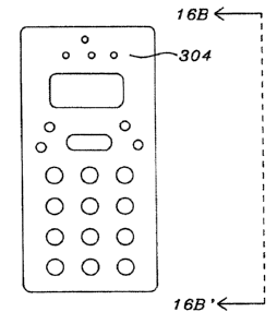
Fig. 16A shows a top view of a casing for an electronic communication
device, such as a cell phone, all or part of which is formed of conductive
loaded
resin-based material. Fig 16A shows the top element 304 of the casing. Fig.
16B shows
a side view, as viewed from line 16B-16B' of Fig. 16A, of the casing showing
the side
element 306 and bottom element 302. Part or all of the top element 304, bottom
element
302, and side element 306 can be fabricated from conductive loaded resin-based
materials. Fig 16C shows a cross section view, viewed from line I6C-I6C' of
Fig. 16B
showing segments of the side element 306. As shown in Fig. 16C an antenna
ele~.ent
308 and an EMF absorbing element 310 can be embedded in the side element 306.
As
shown in Fig. 16C, insulation elements 309 must be used to insulate the
antenna element
308 from the EMF absorbing element 310.
22
CA 02457610 2004-02-13
INT-03-001
Fig. 17A shows a top view and Fig. 17B shows a cross section view, taken
along line 17B-17B' of Fig. 17A, of a EMF absorbing integrated circuit package
formed
of conductive loaded resin-based material. Figs. 17A and 17B show a first
package
element 318 in which an insulating substrate 324 is embedded. A number of
integrated
circuit elements 326 are mounted on the substrate 324. In the example shown in
Fig. 17B
three integrated circuit elements are shown as an example however the number
of
integrated circuit elements could be more or less than three. Electronic
circuit traces, not
shown, can be formed on the substrate 324 to interconnect the integrated
circuit elements
326. Inputloutput leads 314 are used to bring electrical signals into and out
from the
integrated circuit elements 326. A second package element 312 then covers the
assembly,
as shown in Fig. 17B, and is joined to the first package element 318.
Insulation material
320 must be used to insulate the input/output leads 314 from both the first
package
element 318 and the second package element 312. The first package element 318
and the
second package element 312, both formed from conductive loaded resin-based
materials
provide electromagnetic absorption for the assembly in the package.
Antennas formed from the conductive loaded resin-based materials can be
designed to work at frequencies from about 2 Kilohertz to about 300 Gigahertz
or any
other allocated radio frequencies. The geometries scale linearly with the
frequencies of
application, the higher the frequency the smaller the dimensions. Antennas
formed from
conductive loaded resin-based materials can receive signals, which are
horizontally,
vertically, circularly, or cross polarized.
23
CA 02457610 2004-02-13
INT-03-001
The conductive loaded resin-based materials could also be formed as
probes for oscilloscopes and other electronic instruments in place of metal
probes.
While the invention has been particularly shown and described with
reference to the preferred embodiments thereof, it will be understood by those
skilled in
the art that various changes in form and details may be made without departing
from the
spirit and scope of the invention.
24