Note: Descriptions are shown in the official language in which they were submitted.
CA 02457869 2004-02-17
WO 03/021728 PCT/US02/27925
1
VERY NARROW BAND, TWO CHAMBER, HIGH REP RATE GAS DISCHARGE
LASER SYSTEM
The present invention claims priority to U.S. Serial No. 10/012,002 filed
November 30,
2001 and is a continuation-in-part of Serial No. 10/006,913, filed November
29, 2001,
Serial No. 09/943,343, filed August 29, 2001, Serial No. 09/854,097, filed May
11,
2001, Serial No. 09/848,043, filed May 3, 2001, Serial No. 09/459,165, filed
December
10, 1999, Serial No. 09/794,782, filed February 27, 2001, Serial No.
09/771,789, filed
January 29, 2001, Serial No. 09/768,753, filed January 23, 2001, Serial No.
09/684,629,
filed October 6, 2000, Serial No. 09/597,812, filed June 19, 2000 and Serial
No.
09/473,852, filed December 27, 1999. This invention relates to electric
discharge gas
lasers and in particular to very narrow band high repetition rate injection
seeded gas
discharge lasers.
BACKGROUND OF THE INVENTION
Electric Discharge Gas Lasers
Electric discharge gas lasers are well known and have been available since
soon after
lasers were invented in the 1960s. A high voltage discharge between 'two
electrodes
excites a laser gas to produce a gaseous gain medium. A resonance cavity
containing the
gain medium permits stimulated amplification of light which is then extracted
from the
cavity in the form of a laser beam. Many of these electric discharge gas
lasers are
operated in a pulse mode.
Excimer Lasers
Excimer lasers are a particular type of electric discharge gas laser and they
have been
known since the mid 1970s. A description of an excimer laser, useful for
integrated
circuit lithography, is described in U.S. Patent No. 5,023,884 issued June 11,
1991
entitled "Compact Excimer Laser." This patent has been assigned to Applicants'
employer, and the patent is hereby incorporated herein by reference. The
excimer laser
described in Patent '884 is a high repetition rate pulse laser. These excimer
lasers, when
used for integrated circuit lithography, are typically operated in an
integrated circuit
fabrication line "around-the-clock" producing many thousands of valuable
integrated
circuits per hour; therefore, down-time can be very expensive. For this reason
most of
CA 02457869 2004-02-17
WO 03/021728 PCT/US02/27925
2
the components are organized into modules which can be replaced within a few
minutes.
Excimer lasers used for lithography typically must have its output beam
reduced in
bandwidth to a fraction of a picometer. This "line-narrowing" is typically
accomplished
in a line narrowing module (called a "line narrowing package" or "LNP") which
forms
the back of the laser's resonant cavity. This LNP is comprised of delicate
optical
elements including prisms, mirrors and a grating. Electric discharge gas
lasers of the type
described in Patent '884 utilize an electric pulse power system to produce the
electrical
discharges, between the two electrodes. In such prior art systems, a direct
current power
supply charges a capacitor bank called "the charging capacitor" or "CD" to a
predetermined and controlled voltage called the "charging voltage" for each
pulse. The
magnitude of this charging voltage may be in the range of about 500 to 1000
volts in
these prior art units. After Co has been charged to the predetermined voltage,
a solid
state switch is closed allowing the electrical energy stored on Co to ring
very quickly
through a series of magnetic compression circuits and a voltage transformer to
produce
high voltage electrical potential in the range of about 16,000 volts (or
greater) across the
electrodes which produce the discharges which lasts about 20 to 50 ns.
Major Advances In Lithography Light Sources
Excimer lasers such as described in the '884 patent have during the period
1989 to 2001
become the primary light source for integrated circuit lithography. More than
1000 of
these lasers are currently in use in the most modern integrated circuit
fabrication plants.
Almost all of these lasers have the basic design features described in the
'884 patent.
This is:
(1) a single, pulse power system for providing electrical pulses across the
electrodes at pulse rates of about 100 to 2500 pulses per second;
(2) a single resonant cavity comprised of a partially reflecting mirror-type
output coupler and a line narrowing unit consisting of a prism beam
expander, a tuning mirror and a grating;
(3) a single discharge chamber containing a laser gas (either I~rF or ArF),
two
elongated electrodes and a tangential fan for circulating the laser gas
between the two electrodes fast enough to clear the discharge region
between pulses, and
CA 02457869 2004-02-17
WO 03/021728 PCT/US02/27925
3
(4) a beam monitor for monitoring pulse energy, wavelength and bandwidth
of output pulses with a feedback control system for controlling pulse
energy, energy dose and wavelength on a pulse-to-pulse basis.
During the 1989-2001 period, output power of these lasers has increased
gradually and
beam quality specifications for pulse energy stability, wavelength stability
and
bandwidth have also become increasingly tighter. Operating parameters for a'
popular
lithography laser model used widely in integrated circuit fabrication include
pulse energy
at 8 mJ, pulse rate at 2,500 pulses per second (providing an average beam
power of up to
about 20 watts), bandwidth at about 0.5 pm (FWHM) and pulse energy stability
at +/-
0.35%.
There is~ a need for further improvements in these beam parameters. Integrated
circuit
fabricators desire better control over wavelength, bandwidth, higher beam
power with
more precise control over pulse energy. Some improvements can be provided with
the
basic design as described in the '884 patent; however, major improvements with
that
basic design may not be feasible. For example, with a single discharge chamber
precise
control of pulse energy may adversely affect wavelength and/or bandwidth and
vice
versa especially at very high pulse repetition rates.
Injection Seeding
A well-known technique for reducing the band-width of gas discharge laser
systems
(including excimer laser systems) involves the injection of a narrow band
"seed" beam
into a gain medium. In one such system, a laser producing the seed beam called
a
"master oscillator" is designed to provide a very narrow bandwidth beam in a
first
gain medium, and that beam is used as a seed beam in a second gain medium. If
the
second gain medium functions as a power amplifier, the system is referred to
as a~
master oscillator, power amplifier (MOPA) system. If the second gain medium
itself
has a resonance cavity (in which laser oscillations take place), the system is
referred to
as an injection seeded oscillator (ISO) system or a master oscillator, power
oscillator
(MOPO) system in which case the seed laser is called the master oscillator and
the
downstream system is called the power oscillator. Laser systems comprised of
two
separate systems tend to be substantially more expensive, larger and more
complicated
CA 02457869 2004-02-17
WO 03/021728 PCT/US02/27925
4
than comparable single chamber laser systems. Therefore, commercial
application of
these two chamber laser systems has been limited.
What is needed is a better laser design for a pulse gas discharge laser for
operation at
repetition rates in the range of about 4,000 pulses per second or greater,
permitting
precise control of all beam quality parameters including wavelength, bandwidth
and
pulse energy.
SUMMARY OF THE INVENTION
The present invention provides an injection seeded modular gas discharge laser
system
capable of producing high quality pulsed laser beams at pulse rates of about
4,000 Hz
or greater and at pulse energies of about 5 to 10 mJ or greater for integrated
outputs of
about 20 to 40 Watts or greater. Two separate discharge chambers are provided,
one
of which is a part of a master oscillator producing a very narrow band seed
beam
which is amplified in the second discharge chamber. The chambers can be
controlled
separately permitting optimization of wavelength parameters in the master
oscillator
and optimization of pulse energy parameters in the amplifying chamber. A
preferred
embodiment is an ArF excimer laser system configured as a MOPA and
specifically
designed for use as a light source for integrated circuit lithography. In this
preferred
embodiment, both of the chambers and the laser optics are mounted on a
vertical
optical table within a laser enclosure. In the preferred MOPA embodiment, each
chamber comprises a single tangential fan providing sufficient gas flow to
permit
operation at pulse rates of 4000 Hz or greater by clearing debris from the
discharge
region in less time than the approximately 0.25 milliseconds between pulses.
The
master oscillator is equipped with a line narrowing package having a very fast
tuning
mirror capable of controlling centerline wavelength on a pulse-to-pulse basis
at
repetition rates of 4000 Hz or greater and providing a bandwidth of less than
0.2 pm
(FWHM). This preferred embodiment also includes a pulse multiplying module
dividing each pulse from the power amplifier into either two or four pulses in
order to
reduce substantially deterioration rates of lithography optics. Other
preferred
embodiments are configured as KrF or FZ MOPA laser systems. Preferred
CA 02457869 2004-02-17
WO 03/021728 PCT/US02/27925
embodiments of this invention utilize a "three wavelength platform" . This
includes an
enclosure optics table and general equipment layout that is the same for each
of the
three types of discharge laser systems expected to be in substantial use for
integrated
circuit fabrication during the early part of the 21S' century, i.e., KrF, ArF,
and Fz
lasers.
BRIEF DESCRIPTION OF THE DRAWINGS
FIG. 1 is a perspective drawing of a preferred embodiment of the present
invention.
FIGS. 1A and 1B show a U-shaped optical table.
FIGS. 1 C and 1 C 1 show a second preferred embodiment.
FIG. 1D show a third preferred embodiment.
FIGS. 2 and 2A show chamber features.
FIGS. 3A and 3B show a two-pass MOPA.
FIGS. 4, 4A, 4B and 4C show features of a preferred pulse power system.
FIGS. 5A, SB, SC1, SC2, SC3 and SD show additional pulse power features.
FIGS. 6A1 and 6A2 show various MOPA configurations and test results.
FIGS. 6B, 6C, 6D and 6E show test results of prototype MOPA systems.
FIGS. 7,~ 7A, 8, 9A, 9B, 10, 10A, 11, 12, 12A, 12B show features of pulse
power
components.
FIG. 13 shows a technique for minimizing fitter problems.
FIG. 14 shows elements of a wavemeter.
FIGS. 14A, 14B, 14C and 14D demonstrate a technique for measuring bandwidth.
FIGS. 14E-H show features of etalons used for bandwidth measurement.
FIG. 15 shows a technique for fast reading of a photodiode array.
FIG. 16 shows a technique for fine line narrowing of a master oscillator.
FIGS. 16A and 16B show a PZT controlled LNP.
FIG. 16C shows the result of the use of the PZT controlled LNP.
FIGS. 16D and 16E show techniques for controlling the LNP.
FIGS. 17, 17A, 17B and 17C show techniques for purging a grating face.
FIG. 18 shows a fan motor drive arrangement.
FIG. 18A show a preferred fan blade.
FIGS. 19 and 19A through 19G show features of a purge system.
FIGS. 20, 20A and 20B show features of a preferred shutter.
CA 02457869 2004-02-17
WO 03/021728 PCT/US02/27925
6
FIGS. 21 and 21A show heat exhanger features.
FIGS. 22A through 22D show features of a pulse multiplier unit.
FIGS. 23, 23A and 23B show a technique for spatially filtering a seed beam.
DETAILED DESCRTPTION OF PREFERRED EMBODIMENTS
FIRST PREFERRED EMBODIMENT
Three Wavelength Platform
First General Layout
FIG. 1 is a perspective view of a first preferred embodiment of the present
invention.
This embodiment is an injection seeded narrow band excimer laser system
configured as
a MOPA laser system. It is specially designed for use as a light source for
integrated
circuit lithography. The major improvement in the present invention as
exemplified in
this embodiment over the prior art lithography lasers is the utilization of
injection
seeding and in particular a master oscillator-power amplifier (MOPA)
configuration with
two separate discharge chambers.
This first preferred embodiment is an argon-fluoride (ArF) excimer laser
system;
however, the system utilizes a modular platform configuration which is
designed to
accommodate either krypton-fluoride (KrF), ArF or fluorine (Fa) laser
components. This
platform design permits use of the same basic cabinet and many of the laser
system
modules and components for either of these three types of lasers. Applicants
refer to this
platform as their "three wavelength platform" since the three laser designs
produce laser
beams with wavelengths of about 248 nm for I~rF, about 193 nm for ArF and
about
157.63 for F2. This platform is also designed with interface components to
make the
laser systems at each of the three wavelengths compatible with modern
lithography tools
of all the major makers of such tools. Preferred ArF product options includes:
Rep Rate Pulse EnergyPulse Duration
4 kHz 7 mJ 60 ns
4 kHz 7 mJ 100 ns
4 kHz 10 mJ 60 ns
4 kHz 12 mJ 30 ns
CA 02457869 2004-02-17
WO 03/021728 PCT/US02/27925
The major components of this preferred laser system 2 are identified in FIG.
1. These
include:
(1) laser system frame 4 which is designed to house all modules of the laser '
except the AC/DC power supply module,
(2) the AC/DC high voltage power supply module 6,
(3) a resonant charger module 7 for charging two charging capacitor banks to
about 1000 volts at rates of 4000 charges per second,
(4) two commutator modules 8A and 8B each comprising one of the charging
capacitor banks referred to above and each comprising a commutator
circuit for forming very short high voltage electrical pulses, of about
16,000 volts and about 1 ~s duration from the energy stored on the
charging capacitor banks,
(5) two discharge chamber modules mounted in a top bottom configuration in
frame 4 consisting of a master oscillator module 10 and a power amplifier
module 12. Each module includes a discharge chamber 10A and 12A and
a compression head lOB and 12B mounted on top of the chamber. The
compression head compresses (time-wise) the electrical pulses from the
commutator module from about 1 ~,s to about 50 ns with a corresponding
increase in current,
(6) master oscillator optics including line narrowing package lOC and output
coupler unit l OD,
(7) a wavefront engineering box 14 including optics and instruments for
shaping and directing the seed beam into the power amplifier, and
monitoring the MO output power,
(8) beam stabilizer module 16 including wavelength, bandwidth and energy
monitors,
(9) shutter module 18,
(10) an auxiliary cabinet in which are located a gas control module 20, a
cooling water distribution module 22 and an air ventilation module 24,
(11)a customer interface
module 26,
(12)a laser control module
28, and
(13)a status lamp 30
CA 02457869 2004-02-17
WO 03/021728 PCT/US02/27925
8
This preferred embodiment which is described in great detail herein is an ArF
MOPA
configuration as stated above. Some of the changes needed to convert this
specific
configuration to other configurations are the following. The MOPA design can
be
converted to MOPO design by creating a resonance cavity around the second
discharge
chamber. Many techniques are available to do this some of which are discussed
in the
patent applications incorporated by reference herein. I~rF laser designs tend
to be very
similar to ArF designs, so most of the features described herein are directly
applicable to
I~rF. In fact, the preferred grating used for ArF operation works also for
I~rF since the
wavelengths of both lasers correspond to integer multiples of the line spacing
of the
grating.
When this design is used for F2 lasers either MOPA or MOPO, preferably a line
selector
unit is used instead of the LNP described herein since the natural F2 spectrum
comprises
two primary lines one of which is selected and the other of which is
deselected.
U-Shaped Optical Table
Preferably the optics of both the MO and the PA are mounted on a U-shaped
optical
table as shown in FIGS. 1A and 1B. The U-shaped optical table is kinematically
mounted to the base of the laser in the manner described in U.S. Patent No.
5,863,017
incorporated herein by reference. Both chambers of the MO and the PA are not
mounted
on the table but each is supported by three wheels (two on one side and one on
the other)
on rails supported from the bottom frame of chamber 2. (The wheel and rails
are
preferably arranged as described in U.S. Patent No. 6,109,574 incorporated
herein by
reference.) This arrangement provides isolation of the optics from chamber
caused
vibrations.
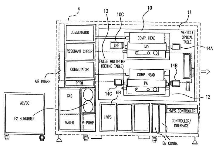
Second General Layout
A second general layout shown in FIG. 1 C is similar to the first general
layout described
above but including the following features:
(1) the two chambers and the laser optics are mounted on a vertical optical
table 11 which is kinematically mounted (as described in a following
section) within the laser cabinet 4. The chambers are supported on stiff
CA 02457869 2004-02-17
WO 03/021728 PCT/US02/27925
9
cantilever arms bolted to the optical table. In this design the master
oscillator 10 is mounted above the power amplifier 12.
(2) The high voltage power supply 6B is contained within laser cabinet 4.
This two chamber-ArF 4000 Hz needs only a single 1200 volt power
supply. The laser cabinet, however, is provided with space for two
additional high voltage power supplies which will be needed for a two
chamber, 6000 Hz, F2 laser system. One additional HVPS will be utilized
for a 6000 Hz ArF system.
(3) Each of the two laser chambers and the pulse power supplies for the
chambers are substantially identical to the chamber and pulse power
supply utilized in a 4000 Hz single chamber laser system described
United States Patent Application Serial No. 09/854,097 which has been
incorporated herein by reference.
(4) A pulse multiplier module 13 located behind the optical table 11 is
included in this embodiment to stretch the duration of the pulse exiting
the power amplifier.
(5) The master oscillator beam output optics 14A directs the output beam
from the MO to the power amplifier input-output optics 14B and for two
passes through the power amplifier 12 via power amplifier rear optics
14C. The first pass is at a small angle with the electrodes and the second
pass is aligned with the electrodes, all as described below. The entire
beam path through the laser system including the pulse stretcher is
enclosed in vacuum compatible enclosures (not shown) and the
enclosures are purged with nitrogen or helium.
Third General Layout
Portions of a third general layout is shown in FIG. 1D. This layout
accommodates an
embodiment of the present invention which utilizes laser chambers in which the
length
of the discharge region between the electrodes is about one-half the length
between the
electrodes in the first two embodiments. That is, the discharge region length
is about
26.5 cm as compared to typical length of about 53 cm. In this case, the
resonant cavity
of the master oscillator 10(1) is defined by two passes through the discharge
region
between output coupler lOD and LNP 10C. In this layout, the beam makes four
passes
CA 02457869 2004-02-17
WO 03/021728 PCT/US02/27925
through the power amplifier 12(1). The first pass after reflection from mirror
15A
through the bottom half of the discharge region at an angle with the alignment
of the
electrodes angling from (for example in the bottom half left to right at an
angle of about
10 milliradians). The second pass after reflection from mirrors 15B is through
the top
half at an angle right to left at an angle of about 4 degrees. The third pass
after reflection
from two mirrors 15C is aligned with the electrodes through the top half of
the discharge
region and the last pass after reflection from mirrors 15D is aligned with the
electrodes
through the bottom half of the discharge region. This last pass establishes
the power
amplifier output beam. It bypasses mirrors 15C and is directed by mirrors (not
shown) to
the pulse multiplier unit (also not shown).
In each of the above three layouts provisions are preferably made to permit
the output
beam to exit at the left of the laser enclosure or the right of the enclosure
in order to
accommodate customer preference without major design changes.
In each of the above layouts some improvement in performance could be achieved
by
combining the commutator and the compression head into a single module.
Applicants
have resisted this combination in the past because any component failure
requires
replacement of the entire module. However, Applicants experience is that these
units are
extremely reliable so that the combined module is now feasible. In fact, one
of the few
causes of failure in the pulse power units has been failure of the electrical
cable
connecting the two modules. This cable would not be needed in the combined
module.
The design and operation of the preferred laser systems and the modules
referred to
above are described in more detail below.
The Master Oscillator
The master oscillator 10 shown in FIGS. l and 1 C is in many ways similar to
prior art
ArF lasers such as described in the '884 patent and in U.S. Patent No.
6,128,323 and is
substantially equivalent to the ArF laser described in U.S. Patent Application
Serial No.
09/854,097 except the output pulse energy is about 0.1 mJ instead of about 5
mJ.
However, major improvements over the '323 laser are provided to permit
operation at
4000 Hz and greater. The master oscillator is optimized for spectral
performance
CA 02457869 2004-02-17
WO 03/021728 PCT/US02/27925
11
including bandwidth control. This result is a much more narrow bandwidth and
improved bandwidth stability. The master oscillator comprises discharge
chamber 10A
as shown in FIG. l, FIG. 2 and FIG. 2A in which are located a pair of
elongated
electrodes 10 A-2 and 10A-4, each about 50 cm long and spaced apart by about
0.5 inch.
Anode 10A-4 is mounted on flow shaping anode support bar 10A-6. Four separate
finned water cooled heat exchanger units 10A-8 are provided. A tangential fan
10A-10
is driven by two motors (not shown) for providing a laser gas flow at a
velocity of about
80 m/s between the electrodes. The chamber includes window units (not shown)
with
CaFa windows positioned at about 45° with the laser beam. An
electrostatic filter unit
having an intake at the center of the chamber, filters a small portion of the
gas flow as
indicated at 11 in FIG. 2 and the cleaned gas is directed into window units in
the manner
described in U.S. Patent No. 5,359,620 (incorporated herein by reference) to
keep
discharge debris away from the windows. The gain region of the master
oscillator is
created by discharges between the electrodes through the laser gas which in
this
embodiment is comprised of about 3% argon, 0.1% FZ and the rest neon. The gas
flow
clears the debris of each discharge from the discharge region prior to the
next pulse.
The resonant cavity is created at the output side by an output coupler lOD
which is
comprised of a CaF2 mirror mounted perpendicular to the beam direction and
coated to
reflect about 30% of light at 193 nm and to pass about 70% of the 193 nm
light. The
opposite boundary of the resonant cavity is a line narrowing unit l OC as
shown in FIG. 1
similar to prior art line narrowing units described in U.S. Patent No.
6,128,323. The
LNP is described in more detail below as in FIGS. 16, 16A, 16B1 and 16B2.
Important
improvements in this line narrowing package include four CaF beam expanding
prisms
lOCl for expanding the beam in the horizontal direction by 45 times and a
tuning mirror
10C2 controlled by a stepper motor for relatively large pivots and a
piezoelectric driver
for providing extremely fine tuning of the mirror echelle grating 10C3 having
about 80
facets per mm is mounted in the Litrow configuration reflects a very narrow
band of UV
light selected from the approximately 300 pm wide ArF natural spectrum.
Preferably
the master oscillator is operated at a much lower F2 concentration than is
typicaly used
in prior art lithography light sources. This results in substantial reductions
in the
bandwidth. Another important improvement is a narrow rear aperture which
limits the
cross section of the oscillator beam to 1.1 mm in the horizontal direction and
7 mm in the
vertical direction. Control of the oscillator beam is discussed below.
CA 02457869 2004-02-17
WO 03/021728 PCT/US02/27925
12
In preferred embodiments the main charging capacitor banks for both the master
oscillator and the power amplifier are charged in parallel so as to reduce
fitter problems.
This is desirable because the time for pulse compression in the pulse
compression
circuits of the two pulse power systems is dependent on the level of the
charge of the
charging capacitors. Preferably pulse energy output is controlled on a pulse-
to-pulse
basis.by adjustment of the chaxging voltage. This limits somewhat the use of
voltage to
control beam parameters of the master oscillator. However, laser gas pressure
and F2
concentration can be easily controlled to achieve desirable beam parameters
over a wide
range pulse energy increases and laser gas pressure. Bandwidth decreases with
F2
concentration and laser gas pressure. These control features are in addition
to the LNP
controls which are discussed in detail below. For the master oscillator the
time between
discharge and light-out is a function of F2 concentration (1 ns/kPa), so F2
concentration
may be changed to vary the timing.
Power Amplifier
The power amplifier in each of the three embodiments is comprised of a laser
chamber
which is very similar to the corresponding master oscillator discharge
chamber. Having
the two separate chambers allows the pulse energy and integrated energy in a
series of
pulses (called dose) to be controlled, to a large extent, separately from
wavelength and
bandwidth. This permits better dose stability. All of the components of the
chamber are
the same and are interchangeable during the manufacturing process. However, in
operation, the gas pressure is substantially lower in the MO as compared to
the PA. The
compression head 12B of the power amplifier is also substantially identical in
this
embodiment to the lOB compression head and the components of the compression
head
are also interchangeable during manufacture. One difference is that the
capacitors of the
compression head capacitor bank axe more widely positioned for the MO to
produce a
substantially higher inductance as compared to the PA. This close identity of
the
chambers and the electrical components of the pulse power systems helps assure
that the
timing characteristics of the pulse forming circuits are the same or
substantially the same
so that fitter problems are minimized.
CA 02457869 2004-02-17
WO 03/021728 PCT/US02/27925
13
The power amplifier is configured for two beam passages through the discharge
region
of the power amplifier discharge chamber in the FIG. 1 and FIG. 1 C
embodiments and
for four passages in its FIG. 1D embodiment as described above. FIGS. 3A and
3B
show the beam path through the master oscillator and the power amplifier for
the FIG. 1
embodiment. The beam oscillates several times through the chamber 10A and LNP
l OC
of the MO 10 as shown in FIG. 3A and is severely line narrowed on its passages
through
LNP l OC. The line narrowed seed beam is reflected upward by mirror 14A and
reflected
horizontally at an angle slightly skewed (with respect to the electrode
orientations)
through chamber 12A by mirror 14B. At the back end of the power amplifier two
mirrors 12C and 12D reflect the beam back for a second pass through PA chamber
12A
horizontally in line with the electrode orientation as shown in FIG. 3B.
The charging voltages preferably are selected on a pulse-to-pulse basis to
maintain
desired pulse and dose energies. F2 concentration and laser gas pressure can
be adjusted
to provide a desired operating range of charging voltage. This desired range
can be
selected to produce a desired value of dE/dV since the change in energy with
voltage is a
function of F2 concentration and laser gas pressure. The timing of injections
is
preferable based on charging voltage. The frequency of injections preferably
is
preferably high to keep conditions relatively constant and can be continuous
or nearly
continuous. Some users of these embodiments may prefer larger durations (such
as 2
hours) between F2 injections.
Test Results
Applicants have conducted extensive testing of the basic MOPA configuration
shown in
FIG.1 with various optical paths as shown in FIG. 6A1. FIGS.6A2 through 6E
display
some of the results of this proof of principal testing.
FIG. 6A shows how well the skewed double pass amplifier design performs as
compared
with other amplifier designs. Other designs that have been tested are single
pass, straight
double pass, single pass with divided amplifier electrodes, tilted double
pass. FIG. 6B
shows system output pulse energy as a function of PA input energy for the
skewed
double pass configuration at charging voltage ranging from 650 V to 1100 V.
FIG. 6C
shows the shape of the output pulse as a function of time delay between
beginning of the
CA 02457869 2004-02-17
WO 03/021728 PCT/US02/27925
14
oscillator and the amplifier pulses for four input energies. FIG. 6D shows the
effect of
time delay between pulses on output beam bandwidth. This graph also shows the
effect
of delay on output pulse energy. This graph shows that bandwidth can be
reduced at the
expense of pulse energy. FIG. 6E shows that the laser system pulse duration
can also be
extended somewhat at the expense of pulse energy.
Pulse Power Circuit
In the preferred embodiment shown in FIGS. 1, 1C and 1D, the basic pulse power
circuits are similar to pulse power circuits of prior art excimer laser light
sources for
lithography. However, separate pulse power circuits downstream of the charging
capacitors are provided for each discharge chamber. Preferably a single
resonant charger
charges two charging capacitor banks connected in parallel to assure that both
charging
capacitor banks are charged to precisely the same voltage. Important
improvements are
also provided to regulate the temperature of components of the pulse power
circuits. In
preferred embodiments the temperatures of the magnetic cores of saturable
inductors are
monitored and the temperature signals are utilized in a feedback circuit to
adjust the
relative timing of the discharge in the two chambers. FIGS. 5A and SB show
important
elements of a preferred basic pulse power circuit which is used for the MO.
The same
basic circuit is also used for the PA.
Resonant Charger
A preferred resonant charger system is shown in FIG. 5B. The principal circuit
elements
are:
I1 - A three-phase power supply 300 with a constant DC current output.
C-1 - A source capacitor 302 that is an order of magnitude or more larger than
the existing Co capacitor 42.
Q1, Q2, and Q3 - Switches to control current flow for charging and maintaining
a regulated voltage on Co.
D1, D2, and D3 - Provides current single direction flow.
R1, and R2 - Provides voltage feedback to the control circuitry.
R3 - Allows for rapid discharge of the voltage on Co in the event of a small
over
charge.
CA 02457869 2004-02-17
WO 03/021728 PCT/US02/27925
Ll - Resonant inductor between C-1 capacitor 302 and Co capacitor banks 42 to
limit current flow and setup charge transfer timing.
Control Board 304 - Commands Q1, Q2, and Q3 open and closed based upon
. circuit feedback parameters.
This circuit includes switch Q2 and diode D3, together known as a De-Qing
switch.
This switch improves the regulation of the circuit by allowing the control
unit to short
out the inductor during the resonant charging process. This "de-qing" prevents
additional energy stored in the current of the charging inductor, L1, from
being
transferred to capacitor Co.
Prior to the need for a laser pulse the voltage on C-1 is charged to 600-800
volts and
switches Q1-Q3 are open. Upon command from the laser, Q1 would close. At this
time
current would flow from C-1 to Co through the charge inductor L1. As described
in the
previous section, a calculator on the control board would evaluate the voltage
on Co and
the current flowing in L 1 relative to a command voltage set point from the
laser. Q 1 will
open when the voltage on the CO capacitor banks plus the equivalent energy
stored in
inductor Ll equals the desired command voltage. The calculation is:
Vf = L '' COs2 + ~~Ll ~ ILIs2OC0O0.5
Where:
V f = The voltage on Co after Q 1 opens and the current in L l goes to zero.
Vcos = The voltage on Co when Ql opens.
I Lis = The current flowing through L1 when Q1 opens.
After Q1 opens the energy stored in L1 starts transferring to the CO capacitor
banks
through D2 until the voltage on the CO capacitor banks approximately equals
the
command voltage. At this time Q2 closes and current stops flowing to CO and is
directed through D3. In addition to the "de-qing" circuit, Q3 and R3 from a
bleed-down
circuit allow additional fine regulation of the voltage on CO.
Switch Q3 of bleed down circuit 216 will be commanded closed by the control
board
when current flowing through inductor L1 stops and the voltage on Co will be
bled down
CA 02457869 2004-02-17
WO 03/021728 PCT/US02/27925
16
to the desired control voltage; then switch Q3 is opened. The time constant of
capacitor
C° and resistor R3 should be sufficiently fast to bleed down capacitor
C° to the command
voltage without being an appreciable amount of the total charge cycle.
As a result, the resonant charger can be configured with three levels of
regulation
control. Somewhat crude regulation is provided by the energy calculator and
the
opening of switch Q1 during the charging cycle. As the voltage on the CO
capacitor
banks nears the target value, the de-qing switch is closed, stopping the
resonant charging
when the voltage on C° is at or slightly above the target value. In a
preferred
embodiment, the switch Q 1 and the de-qing switch is used to provide
regulation with
accuracy better than +l- 0.1 %. If additional regulation is required, the
third control over
the voltage regulation could be utilized. This is the bleed-down circuit of
switch Q3 and
R3 (shown at 216 in FIG. 5B) to discharge the CO's down to the precise target
value.
Improvements Downstream of the CO's
As indicated above, the pulse power system of the MO and the PA of the present
invention each utilizes the same basic design (FIG. 5A) as was used in the
prior art
systems. However, some significant improvements in that basic design were
required for
the approximate factor of 3 increase in heat load resulting from the greatly
increased
repetition rate. These improvements are discussed below.
Detailed Commutator and Compression Head Description
In this section, we describe details of fabrication of the commutator and the
compression
head.
Solid State Switch
Solid state switch 46 is an P/N CM 800 HA-34H IGBT switch provided by Powerex,
Inc. with offices in Youngwood, Pennsylvania. In a preferred embodiment, two
such
switches are used in parallel.
Inductors
Inductors 48, 54 and 64 are saturable inductors similiar to those used in
prior systems as
described in U.S. Patents 5,448,580 and 5,315,611. FIG. 7 shows a preferred
design of
the L° inductor 48. In this inductor four conductors from the two IGBT
switches 46B
CA 02457869 2004-02-17
WO 03/021728 PCT/US02/27925
17
pass through sixteen ferrite toroids 49 to form part 48A an 8 inch long hollow
cylinder of
very high permability material with an ID of about 1 inch and an Od of about
1.5 inch.
Each of the four conductors are then wrapped twice around an insulating
doughnut
shaped core to form part 48B. The four conductors then connect to a plate
which is in
turn connected to the high voltage side of the C1 capacitor bank 52.
A preferred sketch of saturable inductor 54 is shown in FIG. 8. In this case,
the inductor
is a single turn geometry where the assembly top and bottom lids 541 and 542
and center
mandrel 543, all at high voltage, form the single turn through the inductor
magnetic
cores. The outer housing 545 is at ground potential. The magnetic cores are
0.0005"
thick tape wound 50-50% Ni-Fe alloy provided by Magnetics of Butler,
Pennsylvania or
National Arnold of Adelanto, California. Fins 546 on the inductor housing
facilitate
transfer of internally dissipated heat to forced air cooling. In addition, a
ceramic disk
(not shown) is mounted underneath the reactor bottom lid to help transfer heat
from the
center section of the assembly to the module chassis base plate. FIG. 8 also
shows the
high voltage connections to one of the capacitors of the C1 capacitor bank 52
and to a
high voltage lead on one of the induction units of the 1:25 step up pulse
transformer 56.
The housing 545 is connected to the ground lead of unit 56.
A top and section view of the saturable inductor 64 is shown respectively in
FIGS. 9A
and 9B. In the inductors of this embodiment, flux excluding metal pieces 301,
302, 303
and 304 are added as shown in FIG. 9B in order to reduce the leakage flux in
the
inductors. These flux excluding pieces substantially reduce the area which the
magnetic
flux can penetrate and therefore help to minimize the saturated inductance of
the
inductor. The current makes five loops through vertical conductor rods in the
inductor
assembly around magnetic core 307. The current enters at 305 travels down a
large
diameter conductor in the center labeled "1" and up six smaller conductors on
the
circumference also labeled "1" as shown in FIG. 9A. The current then flows
down two
conductors labeled 2 on the inside, then up the six conductors labeled 2 on
the outside
then down flux exclusion metal on the inside then up the six conductors
labeled 3 on the
outside, then down the two conductors labeled 3 on the inside, then up the six
conductors
labeled 4 on the outside, then down the conductor labeled 4 on the inside. The
flux
exclusion metal components are held at half the full pulsed voltage across the
conductor
CA 02457869 2004-02-17
WO 03/021728 PCT/US02/27925
18
allowing a reduction in the safe hold-off spacing between the flux exclusion
metal parts
and the metal rods of the other turns. The magnetic core 307 is made up of
three coils
307A, B and C formed by windings of 0.0005" thick tape 80-20% Ni-Fe alloy
provided
by Magnetics, Inc. of Butler, Pennsylvania or National Arnold of Adelanto,
California.
The reader should note that nano-crystoline materials such as VITROPERMTM
available
from VACUUM SCHITELZE GmbH, Germany and F1NEMETTM from Hitachi Metals,
Japan could be used for inductors 54 and 64.
In prior art pulse power systems, oil leakage from electrical components has
been a
potential problem. In this preferred embodiment, oil insulated components are
limited to
the saturable inductors. Furthermore, the saturable inductor 64 as shown in
FIG. 9B is
housed in a pot type oil containing housing in which all seal connections are
located
above the oil level to substantially eliminate the possibility of oil leakage.
For example,
the lowest seal in inductor 64 is shown at 308 in FIG. 8B. Since the normal
oil level is
below the top lip of the housing 306, it is almost impossible for oil to leak
outside the
assembly as long as the housing is maintained in an upright condition.
Capacitors
Capacitor banks 42, 52, 62 and 82 (i.e., C°, C1, Cp_1 and Cp) as shown
in FIG. 5 are all
comprised of banks of off the-shelf capacitors connected in parallel.
Capacitors 42 and
52 are film type capacitors available from suppliers such as Vishay
Roederstein with
offices in Statesville, North Carolina or Wima of Germany. Applicants
preferred method
of connecting the capacitors and inductors is to solder them to positive and
negative
terminals on special printed circuit board having heavy nickel coated copper
leads in a
manner similar to that described in U.S. Patent No. 5,448,580. Capacitor bank
62 and 64
is typically composed of a parallel array of high voltage ceramic capacitors
from vendors
such as Murata or TDK, both of Japan. In a preferred embodiment for use on
this ArF
laser, capacitor bank 82 (i.e., Cp) comprised of a bank of thirty three 0.3 nF
capacitors
for a capacitance of 9.9 nF; Cp_i is comprised of a bank of twenty four 0.40
nF
capacitors for a total capacitance of 9.6 nF; C1 is a 5.7 ~F capacitor bank
and C° is a 5.3
~,F capacitor bank.
CA 02457869 2004-02-17
WO 03/021728 PCT/US02/27925
19
Pulse Transformer
Pulse transformer 56 is also similar to the pulse transformer described in
U.S. Patent
Nos. 5,448,580 and 5,313,481; however, the pulse transformers of the present
embodiment has only a single turn in the secondary winding and 24 induction
units
equivalent to 1/24 of a single primary turn for an equivalent step-up ratio of
1:24. A
drawing of pulse transformer 56 is shown in FIG. 10. Each of the 24 induction
units
comprise an aluminum spool 56A having two flanges (each with a flat edge with
threaded bolt holes) which are bolted to positive and negative terminals on
printed circuit
board 56B as shown along the bottom edge of FIG. 10. (The negative terminals
are the
high voltage terminals of the twenty four primary windings.) Insulators 56C
separates
the positive terminal of each spool from the negative terminal of the adjacent
spool.
Between the flanges of the spool is a hollow cylinder 1 1/16 inches long with
a 0.875 OD
with a wall thickness of about 1/32 inch. The spool is wrapped with one inch
wide, 0.7
mil thick MetglasTM 2605 S3A and a 0.1 mil thick mylar film until the OD of
the
insulated MetglasTM wrapping is 2.24 inches. A prospective view of a single
wrapped
spool forming one primary winding is shown in FIG. 10A.
The secondary of the transformer is a single OD stainless steel rod mounted
within a
tight fitting insulating tube of PTFE (Teflono). The winding is in four
sections as shown
in FIG. 10. The low voltage end of stainless steel secondary shown as 56D in
FIG. 10 is
tied to the primary HV lead on printed circuit board 56B at 56E, the high
voltage
terminal is shown at 56F. As a result, the transformer assumes an auto-
transformer
configuration and the step-up ratio becomes 1:25 instead of 1:24. Thus, an
approximately
-1400 volt pulse between the + and - terminals of the induction units will
produce an
approximately -35,000 volt pulse at terminal 56F on the secondary side. This
single turn
secondary winding design provides very low leakage inductance permitting
extremely
fast output rise time.
Details of Laser Chamber Electrical Components
The Cp capacitor 82 is comprised of a bank of thirty-three 0.3 of capacitors
mounted on
top of the chamber pressure vessel. (Typically an ArF laser is operated with a
lasing gas
made up of 3.5% argon, 0.1% fluorine, and the remainder neon.) The electrodes
are
about 28 inches long which are separated by about 0.5 to 1.0 inch preferably
about 5l8
CA 02457869 2004-02-17
WO 03/021728 PCT/US02/27925
inch. Preferred electrodes are described below. In this embodiment, the top
electrode is
referred to as the cathode and the bottom electrode is connected to ground as
indicated in
FIG. 5 and is referred to as the anode.
Discharge Timing
In ArF, I~rF and F2 electric discharge lasers, the electric discharge lasts
only about 50 ns
(i.e., 50 billionths of a second). This discharge creates a population
inversion necessary
for lasing action but the inversion only exists during the time of the
discharge.
Therefore, an important requirement for an injection seeded ArF, KrF or F2
laser is to
assure that the seed beam from the master oscillator passes through discharge
region of
the power amplifier during the approximately 50 billionth of a second when the
population is inverted in the laser gas so that amplification of the seed beam
can occur.
An important obstacle to precise timing of the discharge is the fact that
there is a delay
of about 5 microseconds between the time switch 42 (as shown in FIG. 5) is
triggered to
close and the beginning of the discharge which lasts only about 40 - 50 ns. It
takes this
approximately 5 microseconds time interval for the pulse to ring through the
circuit
between the Co's and the electrodes. This time interval varies substantially
with the
magnitude of the charging voltage and with the temperature of the inductors in
the
circuit.
Nevertheless in the preferred embodiment of the present invention described
herein,
Applicants have developed electrical pulse power circuits that provide timing
control of
the discharges of the two discharge chambers within a relative accuracy of
less than
about 2 ns (i.e., 2 billionths of a second). A block diagram of the two
circuits are shown
in FIG. 4.
Applicants have conducted tests which show that timing varies with charging
voltage by
approximately 5 - 10 ns/volt. This places a stringent requirement on the
accuracy and
repeatability of the high voltage power supply charging the charging
capacitors. For
example, if timing control of 5 ns is desired, with a shift sensitivity of 10
ns per volt,
then the resolution accuracy would be 0.5 Volts. For a nominal charging
voltage of 1000
V, this would require a charging accuracy of 0.05% which is very difficult to
achieve
CA 02457869 2004-02-17
WO 03/021728 PCT/US02/27925
21
especially when the capacitors must be charged to those specific values 4000
times per
second.
Applicants' preferred solution to this problem is to charge the charging
capacitor of both
the MO and the PA in parallel from the single resonant charger 7 as indicated
in FIG. 1
and FIG. 4 and as described above. It is also important to design the two
pulse
compression/amplification circuits for the two systems so that time delay
versus
charging voltage curves match as shown in FIG. 4A. This is done most easily by
using
to the extent possible the same components in each circuit.
Thus, in order to minimize timing variations (the variations are referred to
as fitter) in
this preferred embodiment, Applicants have designed pulse power components for
both
discharge chambers with similar components and have confirmed that the time
delay
versus voltage curves do in fact track each other as indicated in FIG. 4A.
Applicants
have confirmed that over the normal operating range of charging voltage, there
is a
substantial change in time delay with voltage but the change with voltage is
virtually the
same for both circuits. Thus, with both charging capacitors charged in
parallel charging
voltages can be varied over a wide operating range without changing the
relative timing
of the discharges.
Temperature control of electrical components in the pulse power circuit is
also important
since temperature variations can affect pulse compression timing (especially
temperature
changes in the saturable inductors). Therefore, a design goal is to minimize
temperature
variations and a second approach is to monitor temperature of the temperature
sensitive
components and using a feedback control adjust the trigger timing to
compensate.
Controls can be provided with a processor programmed with a learning algorithm
to
make adjustments based on historical data relating to past timing variations
with known
operating histories. This historical data is then applied to anticipate timing
changes
based on the current operation of the laser system.
Trigger Control
The triggering of the discharge for each of the two chambers is accomplished
separately
utilizing for each circuit a trigger circuit such as one of those described in
U.S. Patent
No. 6,016,325. These circuits add timing delays to correct for variations in
charging
CA 02457869 2004-02-17
WO 03/021728 PCT/US02/27925
22
voltage and temperature changes in the electrical components of the pulse
power so that
the time between trigger and discharge is held as constant as feasible. As
indicated
above, since the two circuits are basically the same, the variations after
correction are
almost equal (i.e., within about 2 ns of each other).
As indicated in FIGS. 6C, D, and E, performance of this preferred embodiment
is greatly
enhanced if the discharge in the power amplifier occurs about 40 to 50 ns
after the
discharge in the master oscillator. This is because it takes several
nanoseconds for the
laser pulse to develop in the master oscillator and another several
nanoseconds for the
front part of the laser beam from the oscillator to reach the amplifier and
because the rear
end of the laser pulse from the master oscillator is at a much narrower
bandwidth than
the front part. For this reason, separate trigger signals are provided to
trigger switch 46
for each chamber. The actual delay is chosen to achieve desired beam quality
based on
actual performance curves such as those shown in FIGS. 6C, D and E. The reader
should note, for example, that narrower bandwidth and longer pulses can be
obtained at
the expense of pulse energy by increasing the delay between MO trigger and PA
trigger.
Other Techniques To Control Discharge Timing
Since the relative timing of the discharges can have important effects on beam
quality as
indicated in the FIGS. 6C, D and E graphs, additional steps may be justified
to control
the discharge timing. For example, some modes of laser operation may result in
wide
swings in charging voltage or wide swings in inductor temperature. These wide
swings
could complicate discharge timing control.
Monitor Timing
The timing of the discharges can be monitored on a pulse-to-pulse basis and
the time
difference can be used in a feedback control system to adjust timing of the
trigger signals
closing switch 42. Preferably, the PA discharge would be monitored using a
photocell to
observe discharge fluorescence (called ASE) rather than the laser pulse since
very poor
timing could result if no laser beam being produced in the PA. For the MO
either the
ASE or the seed laser pulse could be used.
CA 02457869 2004-02-17
WO 03/021728 PCT/US02/27925
23
Bias Voltage Adjustment
The pulse timing can be increased or decreased by adjusting the bias currents
through
inductors LB1 Lsa and LB3 which provide bias for inductors 4~, 54 and 64 as
shown in
FIG. 5. Other techniques could be used to increase the time needed to saturate
these
inductors. For example, the core material can be mechanically separated with a
very fast
responding PZT element which can be feedback controlled based on a feedback
signal
from a pulse timing monitor.
Adjustable Parasitic Load
An adjustable parasitic load could be added to either or both of the pulse
power circuits
downstream of the CO's.
Additional Feedback Control
Chaxging voltage and inductor temperature signals, in addition to the pulse
timing
monitor signals can be used in feedback controls .to adjust the bias voltage
or core
mechanical separation as indicated above in addition to the adjustment of the
trigger
timing as described above.
Burst Type Operation
Feedback control of the timing is relatively easy and effective when the laser
is operating
on a continuous .basis. However, normally lithography lasers operate in a
burst mode
such as the following to process 20 areas on each of many wafers:
Off for 1 minute to move a wafer into place
4000 Hz for 0.2 seconds to illuminate area 1
Off for 0.3 seconds to move to area 2
4000 Hz for 0.2 seconds to illuminate area 2
Off for 0.3 seconds to move to area 3
4000 Hz for 0.2 seconds to illuminate area 3
4000 Hz for 0.2 seconds to illuminate area 199
Off for 0.3 seconds to move to area 200
4000 Hz for 0.2 seconds to illuminate area 200
Off for one minute to change wafers
4000 Hz for 0.2 seconds to illuminate area 1 on the next wafer, etc.
CA 02457869 2004-02-17
WO 03/021728 PCT/US02/27925
24
This process may be repeated for many hours, but will be interrupted from time-
to-time
for periods longer than 1 minute.
The length of down times will affect the relative timing between the pulse
power
systems of the MO and the PA and adjustment may be required in the trigger
control to
assure that the discharge in the PA occurs when the seed beam from the MO is
at the
desired location. By monitoring the discharges and the timing of light out
from each
chamber the laser operator can adjust the trigger timing (accurate to within
about 2 ns) to
achieve best performance.
Preferably a laser control processor is programmed to monitor the timing and
beam
quality and adjust the timing automatically for best performance. Timing
algorithms
which develop sets of bin values applicable to various sets of operating modes
are
utilized in preferred embodiments of this invention. These algorithms are in
preferred
embodiments designed to switch to a feedback control during continuous
operation
where the timing values for the current pulse is set based on feedback data
collected for
one or more preceding pulse (such as the immediately preceding pulse).
No Output Discharge
Timing algorithms such as those discussed above work very well for continuous
or
regularly repeated operation. However, the accuracy of the timing may not be
good in
unusual situations such as the first pulse after the laser is off for an
unusual period of
time such as 5 minutes. In some situations imprecise timing for the first one
or two
pulses of a burst may not pose a problem. A preferred technique is to
preprogram the
laser so that the discharges of the MO and the PA are intentionally out of
sequence for
one or two pulses so that amplification of the seed beam from the MO is
impossible. For
example, laser could be programmed to trigger the discharge of the PA ~0 ns
prior to the
trigger of the MO. In this case, there will be no significant output from the
laser but the
laser metrology sensors can determine the timing parameters so that the timing
parameters for the first output pulse is precise.
Water Cooling of Components
To accommodate greater heat loads water cooling of pulse power components is
provided in addition to the normal forced air cooling provided by cooling fans
inside the
laser cabinet in order to support operation at this higher average power mode.
CA 02457869 2004-02-17
WO 03/021728 PCT/US02/27925
~5
One disadvantage of water cooling has traditionally been the possibility of
leaks near the
electrical components or high voltage wiring. This specific embodiment
substantially
avoids that potential issue by utilizing a single solid piece of cooling
tubing that is
routed within a module to cool those components that normally dissipate the
majority of
the heat deposited in the module. Since no joints or connections exist inside
the module
enclosure and the cooling tubing is a continuous piece of solid metal (e.g.
copper,
stainless steel, etc.), the chances of a leak occurring within the module are
greatly
diminished. Module connections to the cooling water are therefore made outside
the
assembly sheet metal enclosure where the cooling tubing mates with a quick-
disconnect
type connector.
Saturable Inductor
In the case of the commutator module a water cooled saturable inductor 54A is
provided
as shown in FIG. 11 which is similar to the inductor 54 shown in FIG. 8 except
the fins
of 54 are replaced with a water cooled jacket 54A1 as shown in FIG. 11. The
cooling
line 54A2 is routed within the module to wrap around jacket 54A1 and through
aluminum base plate where the IGBT switches and Series diodes are mounted.
These
three components make up the majority of the power dissipation within the
module.
Other items that also dissipate heat (snubber diodes and resistors,
capacitors, etc.) are
cooled by forced air provided by the two fans in the rear of the module.
Since the jacket 54A1 is held at ground potential, there are no voltage
isolation issues in
directly attaching the cooling tubing to the reactor housing. This is done by
press-fitting
the tubing into a dovetail groove cut in the outside of the housing as shown
at 54A3 and
using a thermally conductive compound to aid in making good thermal contact
between
the cooling tubing and the housing.
Cooling High Voltage Components
Although the IGBT switches "float" at high voltage, they are mounted on an
aluminum
base electrically isolated from the switches by a 1/16 inch thick alumina
plate. The
aluminum base plate which functions as a heat sink and operates at ground
potential and
is much easier to cool since high voltage isolation is not required in the
cooling circuit.
CA 02457869 2004-02-17
WO 03/021728 PCT/US02/27925
26
A drawing of a water cooled aluminum base plate is shown in FIG. 7A. In this
case, the
cooling tubing is pressed into a groove in an aluminum base on which the
IGBT's are
mounted. As with the inductor 54a, thermally conductive compound is used to
improve
the overall joint between the tubing and the base plate.
The series diodes also "float" at high potential during normal operation. In
this case, the
diode housing typically used in the design provides no high voltage isolation.
To
provide this necessary insulation, the diode "hockey puck" package is clamped
within a
heat sink assembly which is then mounted on top of a ceramic base that is then
mounted
on top of the water-cooled aluminum base plate. The ceramic base is just thick
enough
to provide the necessary electrical isolation but not too thick to incur more
than
necessary thermal impedance. For this specific design, the ceramic is 1/16"
thick
alumina although other more exotic materials, such as beryllia, can also be
used to
further reduce the thermal impedance between the diode junction and the
cooling water.
A second embodiment of a water cooled commutator utilizes a single cold plate
assembly which is attached to the chassis baseplate for the IGBT's and the
diodes. The
cold plate may be fabricated by brazing single piece nickel tubing to two
aluminum
"top" and "bottom" plates. As described above, the IGBT's and diodes are
designed to
transfer their heat into the cold plate by use of the previously mentioned
ceramic disks
underneath the assembly. In a preferred embodiment of this invention, the cold
plate
cooling method is also used to cool the IGBT and the diodes in the resonant
charger.
Thermally conductive rods or a heat pipe can also be used to transfer heat
from the
outside housing to the chassis plate.
Detailed Compression Head Description
The water-cooled compression head is similar in the electrical design to a
prior art air-
cooled version (the same type ceramic capacitors are used and similar material
is used in
the reactor designs). The primary differences in this case are that the module
must run at
higher rep-rates and therefore, higher average power. In the case of the
compression head
module, the majority of the heat is dissipated within the modified saturable
inductor 64A.
Cooling the subassembly is not a simple matter since the entire housing
operates with
short pulses of very high voltages. The solution to this issue as shown in
FIGS. 12, 12A
CA 02457869 2004-02-17
WO 03/021728 PCT/US02/27925
27
and 12B is to inductively isolate the housing from ground potential. This
inductance is
provided by wrapping the cooling tubing around two cylindrical forms that
contain a
ferrite magnetic core. Both the input and output cooling lines are coiled
around cylindrical
portions of a ferrite core formed of the two cylindrical portions and the two
ferrite blocks
as shown in FIGS. 12, 12A and 12B.
The ferrite pieces are made from CN-20 material manufactured by Ceramic
Magnetics,
Inc. of Fairfield, New Jersey. A single piece of copper tubing (0.187"
diameter) is press
fit and wound onto one winding form, around the housing 64A1 of inductor 64A
and
around the second winding form. Sufficient length is left at~the ends to
extend through
fittings in the compression head sheet metal cover such that no cooling tubing
joints exist
within the chassis.
The inductor 64A comprises a dovetail groove as shown at 64A2 similar to that
used in
the water-cooled commutator first stage reactor housing. This housing is much
the same
as previous air-cooled versions with the exception of the dovetail groove. The
copper
cooling-water tubing is press fit into this groove in order to make a good
thermal
connection between the housing and the cooling-water tubing. Thermally
conductive
compound is also added to minimize the thermal impedance.
The electrical design of inductor 64A is changed slightly from that of 64
shown in FIGS
9A and 9B. Inductor 64A provides only two loops (instead of five loops) around
magnetic
core 64A3 which is comprised of four coils of tape (instead of three).
As a result of this water-cooled tubing conductive path from the output
potential to
ground, the bias current circuit is now slightly different. As before, bias
current is
supplied by a dc-do converter in the commutator through a cable into the
compression
head. The current passes through the "positive" bias inductor LB2 and is
connected to the
Cp-1 voltage node. The current then splits with a portion returning to the
commutator
through the HV cable (passing through the transformer secondary to ground and
back to
the dc-do converter). The other portion passes through the compression head
reactor Lp-
1 (to bias the magnetic switch) and then through the cooling-water tubing
"negative"
bias inductor LB3 and back to ground and the dc-do converter. By balancing the
CA 02457869 2004-02-17
WO 03/021728 PCT/US02/27925
28
resistance in each leg, the designer is able to ensure that sufficient bias
current is
available for both the compression head reactor and the commutator
transformer.
The "positive" bias inductor LBa is made very similarly to the "negative" bias
inductor
LB3. In this case, the same ferrite bars and blocks axe used as a magnetic
core. However,
two 0.125" thick plastic spacers axe used to create an air gap in the magnetic
circuit so that
the cores do not saturate with the do current. Instead of winding the inductor
with cooling-
water tubing, 18 AWG teflon wire is wound around the forms.
Quick Connections
In this preferred embodiment, three of the pulse power electrical modules
utilize blind
mate electrical connections so that all electrical connections to the portions
of the laser
system are made merely by sliding the module into its place in the laser
cabinet. These
are the AC distribution module, the power supply module and the resonant
charges
module. In each case a male or female plug on the module mates with the
opposite sex
plug mounted at the back of the cabinet. In each case two approximately 3-inch
end
tapered pins on the module guide the module into its precise position so that
the
electrical plugs properly mate. The blind mate connectors such as AMP Model
No.
194242-1 are commercially available from AMP, Inc. with offices in Harrisburg,
Pennsylvania. In this embodiment connectors are for the various power circuits
such as
208 volt AC, 400 volt AC, 1000 Volt DC (power supply out and resonant charges
in) and
several signal voltages. These blind mate connections permit these modules to
be
removed for servicing and replacing in a few seconds or minutes. In this
embodiment
blind mate connections are not used for the commutator module the output
voltage of the
module is in the range of 20 to 30,000 volts. Instead, a typical high voltage
connector is
used.
Discharge Components
FIGS. 2 and 2A show details of an improved discharge configuration utilized in
preferred embodiments of the present invention. This configuration includes an
electrode configuration that Applicants call a blade-dielectric electrode. In
this design,
the anode 10A4 comprises a blunt blade shaped electrode with dielectric spaces
mounted
on both sides of the anode as shown to improve the gas flow in the discharge
region.
CA 02457869 2004-02-17
WO 03/021728 PCT/US02/27925
29
The anode is 26.4 inches long and 0.439 inches high. It is 0.284 inches wide
at the
bottom and 0.141 inches wide at the top. It is attached to flow shaping anode
support bar
10A6 with screws through sockets that allow differential thermal expansion of
the
electrode from its center position. The anode is comprised of a copper based
alloy
preferably C36000, C95400, or C19400. Cathode 10A2 has a cross section shape
as
shown in FIG. 2A which is slightly pointed at the anode facing position. A
preferred
cathode material is C36000. Additional details of this blade dielectric
configuration are
provided in U.S. Patent Application Serial No. 09/768,753 incorporated herein
by
reference. The current return 10A8 in this configuration is comprised of a
single long
section of thin (about 1/16" diameter) copper or brass wire formed into a
whale bone
shaped with 27 ribs equally spaced along the length of electrode, the cross
section of
which is shown in FIGS. 2 and 2A. The wire is clamped into line grooves at the
bottom
of anode and semi-circular grooves at the chamber top inside surface.
Alternate Pulse Power Circuit
A second preferred pulse power circuit is shown in FIGS. 5C1, SC2 and SC3.
This
circuit is similar to the one described above but utilizes a higher voltage
power supply
for charging Co to a higher value. As in the above described embodiments, a
high
voltage pulse power supply unit operating from factory power at 230 or 460
volts AC, is
power source for a fast charging resonant charger as described above and
designed for
precise charging two 2.17 ~F at frequencies of 4000 to 6000 Hz to voltages in
the range
of about 1100 V to 2250 V. The electrical components in the commutator and
compression head for the master oscillator are as identical as feasible to the
corresponding components in the power amplifier. This is done to keep time
responses
in the two circuits as identical as feasible. Switches 46 are banks of two
IGBT switches
each rated at 3300 V and arranged in parallel. The Co capacitor banks 42 is
comprised of
128 0.068 ~,F 1600 V capacitors arranged in 64 parallel legs to provide the
2.17 ~F Co
bank. The Cl capacitor banks 52 are comprised of 136 0.068 ~,F 1600 V
capacitors
arranged in 68 parallel legs to provide a bank capacitance of 2.33 ~,F. The
Cp_1 and Cp
capacitor banks are the same as those described above with reference to FIG.
5. The 54
saturable inductors are single turn inductors providing saturated inductance
of about 3.3
nH with five cores comprised of 0.5 inch thick 50%-50% Ni-Fe with 4.9 inch OD
and
3.8 inch ID. The 64 saturable inductors are two turn inductors providing
saturated
CA 02457869 2004-02-17
WO 03/021728 PCT/US02/27925
inductance of about 38 nH each comprised of 5 cores, 0.5 inch thick made with
80%-
20% Ni-Fe with an OD of 5 inches and an ID of 2.28 inches. Trigger circuits
are
provided for closing IGBT's 46 with a timing accuracy of two nanoseconds. The
master
oscillator is typically triggered about 40 ns prior to the triggering of the
IGBT 46 for
power amplifier. However, the precise timing is preferably determined by
feedback
signals from sensors which measure the timing of the output of the master
oscillator and
the power amplifier discharge.
Alternate Technique For Timing Control
As described earlier, the throughput timing of the magnetic pulse compression
in the
Pulsed Power system is dependent upon the magnetic material properties that
can be a
function of the material temperature, etc. In order to maintain precise
timing, it- is
therefore extremely important to either directly or indirectly monitor and/or
predict these
material properties. One method described previously would utilize temperature
monitors along with previously collected data (delay time as a function of
temperature)
to predict the timing.
An alternate approach would utilize the magnetic switch bias circuit to
actually measure
the magnetic properties (the saturation time) as the magnetics were reverse
biased in
between pulses (or prior to the first pulse). The bias circuit would apply
sufficient
voltage to the magnetic switch to reverse bias the material and at the same
time measure
the saturation time so that the laser timing could be accurately controlled.
Since the volt-
second product utilized in reverse biasing the switch should be equal to that
required
during normal discharge operation in the forward direction, the throughput
delay time of
the Pulsed Power system could be easily calculated knowing the operating
voltage of the
upcoming pulse.
A schematic diagram of the proposed approach is shown in Figure SD. Initial
operation
assumes that the magnetic switch, L1, is already saturated in the forward
direction,
provided by power supply BTl through the two bias isolation inductors, Lbias,
and
switch S4. This current is then interrupted by opening S4 and closing S2 which
applies
~100V to the magnetic switch, Ll, which then saturates after ~30 us. A timer
is
triggered when S2 closes and stops counting when a current probe detects
saturation of
L1, thus calculating the saturation time of L1 for the 100V applied voltage.
L1 is now
CA 02457869 2004-02-17
WO 03/021728 PCT/US02/27925
31
reverse biased and ready for the main pulse discharge sequence once residual
voltage has
been drained from the circuit by S3 and other components.
PULSE LENGTH
As indicated in FIG. 6E, the output pulse length measured in tests conducted
by
Applicants is in the range of about 20 ns and is to some extent a function of
the relative
timing of the two discharges. A longer pulse length (other things being equal)
can
increase the lifetime of optical components of lithography equipment.
Applicants have identified several techniques for increasing pulse length. As
indicated
above, the relative time between discharges can be optimized for pulse length.
The pulse
power circuits of both the MO and the PA could be optimized for longer pulses
using
techniques such as those described in U.S. Patent Application Serial No.
09/451,995
incorporated herein by reference. An optical pulse multiplier system such as
one of
those described in U.S. Patent No. 6,067,311, incorporated by reference
herein, could be
added downstream of the PA to reduce the intensity of individual pulses. A
preferred
pulse multiplier unit is described in the next section. This pulse multiplier
could be
made a part of the beam path to lens components of a lithography tool. The
chamber
could be made longer and the electrodes could be configured to produce
traveling wave
discharges designed for longer pulse lengths.
Pulse Multiplier Unit
A preferred pulse multiplier unit is shown in FIG. 22A. Light beam 20 from
laser 50 hits
the beam splitter 22. Beam splitter has a reflectivity of about 40%. About 40%
of the
light reflects a first portion of the output beam 30. The rest of the incoming
beam
transmits through the beam splitter 22 as beam 24. The beam is reflected back
at a small
angle by a mirror 26, which is a spherical mirror with the focal length equal
the distance
from beam splitter 22 to the mirror. So, the beam is focused to a point 27
near the beam
splitter 22 but missing it slightly. This beam spreads again and is now
reflected by
mirror 28, which is also a spherical mirror with the focal length equal the
distance from
this mirror to point 27. The mirror 28 reflect the beam back at a small angle
and also
collimates the reflected beam. This reflected beam 32 propagates to the right
and is
reflected by mirror 29 to beam splitter 22 where about 60% of the beam is
transmitted
CA 02457869 2004-02-17
WO 03/021728 PCT/US02/27925
32
through beam splitter 22 to merge into and become the second portion of output
beam
30. A portion (about 40%) of beam 34 is reflected by the beam splitter 22 in
the direction
of beam 24 for a repeat of the trip of beam 32. As a result, a short input
pulse is split into
several portions, so that total duration of the beam is increased and its peak
intensity is
decreased. Mirrors 26 and 28 create a relay system which images the portions
of the
outcoming beam onto each other. Because of that imaging, each portion of the
output
beam is virtually the same. (If mirrors 26 and 28 were flat, beam divergence
would
spread the beam for each subsequent repetition, so beam size would be
different for each
repetition.) The total optical path length from beam splitter 22 to mirror 26
to mirror 28
to mirror 27 and, finally, to beam splitter 22 determines the time delay
between
repetitions. FIG. 22B 1 shows the pulse profile of a typical pulse produced by
an ArF
excimer laser. FIG. 22B2 shows the simulated output 'pulse profile of a
similar ArF laser
pulse after being spread in a pulse stretcher built in accordance with FIG. 6.
In this
example the T;S of the pulse was increased from 18.16 ns to 45.78 ns. (T;S is
a measure of
pulse duration used for describing laser pulses. It refers to the integral
square pulse
duration.)
FIG. 22C shows a layout similar to the FIG. 22A layout but with an additional
delay
path. In this case, the first beam splitter 22A is designed for a reflection
of 25 percent
and the second beam splitter 22B is designed for a reflection of 40 percent.
The
resulting beam shape produced by computer simulation is shown in FIG. 22D. The
T;s
for this stretched pulse is about 73.2 ns. In the FIG. 22C embodiment, the
portions of the
beam is transmitted through beam splitter 22B are flipped in orientation when
they return
and are joined into exit beam 30. This reduces significantly the spatial
coherence of the
beam.
FIGS. 22E and F show beam splitter designs which use optical elements without
coatings. FIG. 22E shows a beam splitter design to take advantage of
frustrated internal
reflection and FIG. 22F shows a transparent uncoated plate tilted to produce a
Fresnel
reflection from both sides of the plate to achieve the desired reflection-
transmission
ratio.
CA 02457869 2004-02-17
WO 03/021728 PCT/US02/27925
33
The pulse stretcher unit could be installed in the back of vertical optical
table 11 as
suggested above or it could be installed on top of the table or even inside of
it.
Pulse and Dose Energy Control
Pulse energy and dose energy are preferably controlled with a feedback control
system
and algorithm such as that described above. The pulse energy monitor can be at
the laser
as closer to the wafer in the lithography tool. Using this technique charging
voltages are
chosen to produce the pulse energy desired. In the above preferred embodiment,
both
the MO and the PA are provided with the same charging voltage since the CO's
are
charged in parallel.
Applicants have determined that this technique works very well and greatly
minimize
timing fitter problems. This technique, however, does reduce to an extent the
laser
operator's ability to control the MO independently of the PA. However, there
are a
number of operating parameters of the MO and the PA that can be controlled
reparably
to optimize performance of each unit. These other parameters include: laser
gas
pressure, F2 concentration and laser gas temperature, These parameters
preferably axe
controlled independently in each of the two chambers and regulated in a
processor
controlled feedback arrangement.
Additional Optical Quality Improvement
The present invention provides a laser system capable of much greater pulse
energy and
output power than prior art single chamber high repetition rate gas discharge
lasers.
With this system the master oscillator to a large extent determines the
wavelength and
the bandwidth and the power amplifier primarily controls the pulse energy. The
pulse
energy needed for an efficient seeding of the power amplifier is can be as low
as a small
fraction of a mJ as shown in FIG. 6B. Since the master oscillator type of
laser is easily
capable of producing 5 mJ pulses, it has energy to spare. This additional
pulse energy
provides opportunities for using certain techniques for improving beam quality
which axe
not particularly energy efficient.
CA 02457869 2004-02-17
WO 03/021728 PCT/US02/27925
34
These techniques include:
~ Pulse trimming as described in U.S. Patent No. 5,852,621, incorporated
herein by reference. The pulse energy is monitored, the pulse is delayed and
a portion of the delayed pulse is trimmed using a very fast optical switch
such
as a Pockels cell.
~ Using line-narrowing module with very high beam expansion and small
apertures, as described later in this application.
~ Wavefront engineering
Intercavity wavefront correction in addition to the single bend of the grating
as shown in U.S. Patent No. 6,094,448 can be added to the master oscillator.
This could include multiple bends of the grating as described in U.S. Patent
Application Serial No. 09/703,317 incorporated herein by reference, a
deformable tuning mirror 14, (as described in U.S. Patent No. 6,192,064
incorporated herein by reference), wavefront correction can also be a static
correction such as a non-flat prism face configured to correct a known
wavefront distortion.
~ Beam filtering
Beam filters such as a spacial filter as described in U.S. Patent Application
Serial No. 09/309,478, incorporated by reference herein, and shown at 11 in
FIG. 23 could be added to reduce bandwidth. Beam filters could be within
the MO resonance cavity or between the MO and the PA. The could also be
added downstream of the PA. A preferred spatial filter which does not
require the beam to propogate through a focus is a total internal spatial
filter
and is described in the following section.
~ Coherence control
Coherence of the laser beam can be a problem for integrated circuit
fabricators. Gas discharge lasers typically produce a laser beam which has
low coherence. However, as the bandwidth is made very narrow, a
consequence is greater coherence of the output beam. For this reason, some
induced spacial in-coherence may be desired. Preferably optical components
for reducing the coherence would be added either in the MO resonance cavity
or between the MO and the PA. Several optical components are known for
reducing coherence such as moving phase plates or acoustic-optic devices.
CA 02457869 2004-02-17
WO 03/021728 PCT/US02/27925
~ Aperturing
Beam quality of the seed beam can also be improved by tighter aperturing of
the beam.
Total Internal Spatial Filter
Spatial filtering is effective at reducing the integrated 95% bandwidth.
However, all
direct spatial filtering techniques previously proposed required at least
concentrating the
beam and in most cases actually focusing the beam. Additionally all previous
designs
required multiple optical elements. A simple, compact spatial filter, that
does not require
a focused beam, would be more readily adaptable for incorporation inside the
laser
resonator.
The filter is a single prism approximately 2 inches in length. The entrance
and exit faces
of the prism are parallel to each other and normal to the incident beam. Two
other faces
would.be parallel to each other but orientated at an angle equal to the
critical angle with
respect to the entrance and exit faces. At a wavelength of 193.35 nm the
critical angle in
CaFa is 41.77 degrees. The only coatings required would be normal incidence
anti-
reflection coatings on the entrance and exit faces of the prism.
The spatial filter would work in the following manner. The beam would enter at
normal
incidence to the entrance face of the prism. The beam would then propagate to
the
critical angle face of the prism. If the beam was collimated all rays would be
incident at
the critical angle at this second face. However, if the beam if diverging or
converging
some of the rays will strike this face at angles greater than and less than
the critical
angle. All rays striking this face at or greater than the critical angle will
be reflected at
100%. Rays striking this face at an angle less than the critical angle will be
reflected at
values less than 100% and will be attenuated. All rays that are reflected will
be incident
at the opposite face of the prism at the same angle where they will also be
attenuated by
the same amount. In the design proposed there will be a total of six
reflections for each
pass. The reflectivity for P-polarized light at an angle of 1 mrad less than
the critical
angle is about 71%. Therefore, all rays with incident angles that differ from
the critical
angle by 1 mrad or more will be transmitted at the exit face at less than 13%
of their
original intensity.
CA 02457869 2004-02-17
WO 03/021728 PCT/US02/27925
36
However, a single pass of this filter will only be one sided. All rays that
are incident at
angles greater than the critical angle reflect at 100%. Once exiting the
spatial filter
prism, the beam will be incident upon a mirror. Inside the laser resonator
this mirror
could be the output coupler or the diffraction grating in the LNP. After
reflecting of the
mirror, the rays will re-enter the spatial filter prism, but with one critical
difference. All
rays that exited the spatial filter at angles that were greater than the
critical angle will be
inverted after reflecting off the mirror. These rays will now re-enter the
prism at values
less than the critical angle and will be attenuated. It is this second pass
through the prism
that changes the transmission function of the prism from a one sided filter
into a true
bandpass filter. FIG. 23A shows the theoretical transmission function for a
total internal
reflection spatial filter made from CaF2 at 193.35 nm.
FIG. 23B shows the design of the spatial filter. The input and output faces of
the prism
are.l/2 inch. The critical angle faces are about 2 inches. The input beam
width is 2.6 mm
and represents the width of the beam in the short axis. The prism would have a
height of
1 inch in the plane of the drawing. The figure shows three sets of rays. The
first set of
rays is collimated and strikes the surfaces at the critical angle. These are
the green rays.
A second set of rays is incident at the surface less than the critical angle
and is
terminated at the first reflection. They are the blue rays. These rays are
more visible in
the magnified section. They represent the rays that are attenuated on the
first pass. The
final set of rays is incident at an angle greater than the critical angle.
These rays
propagate through the entire first pass but are terminated at the first
reflection of the
second pass. They represent the rays that are attenuated on the second pass.
Telescope Between Chambers
In preferred embodiments a cylindrical refractive telescope is provided
between the
output of the master oscillator and the input of the power amplifier. This
controls the
horizontal size of the beam entering the power amplifier. This telescope can
also be
designed using well known techniques to control the horizontal divergence.
CA 02457869 2004-02-17
WO 03/021728 PCT/US02/27925
37
Gas Control
The preferred embodiment of this invention has a gas control module as
indicated in
FIG. I and it is configured to fill each chamber with appropriate quantities
of laser gas.
Preferably appropriate controls and processor equipment is provided to
maintain
continuous flow of gas into each chamber so as to maintain laser gas
concentrations
constant or approximately constant at desired levels. This may be accomplished
using
techniques such as those described in U.S. Patent No. 6,028,880 or U.S. Patent
No.
6,151,349 or U.S. Patent No. 6,240,117 (both of which are incorporated hereby
reference).
Another technique for providing continuous flow of laser gas into the chambers
which
Applicants call its binary fill technique is to provide a number (such as 5)
fill lines each
successive line orificed to permit double the flow of the previous line with
each line
having a shut off valve. The lowest flow line is orificed to permit minimum
equilibrium
gas flow. Almost any desired flow rate can be achieved by selecting
appropriate
combinations of valves to be opened. Preferably a buffer tank is provided
between the
orificed lines and the laser gas source which is maintained at a pressure at
about twice
the pressure of the laser chambers.
Variable Bandwidth Control
As described above, this preferred embodiment of the present invention
produces laser
pulses much more narrow than prior art excimer laser bandwidths. In some
cases, the
bandwidth is more narrow than desired giving a focus with a very short depth
of focus.
In some cases, better lithography results are obtained with a larger
bandwidth.
Therefore, in some cases a technique for tailoring the bandwidth will be
preferred. Such
a technique is described in detail in U.S. Patent Application, Serial No.
09/918,773 and
09/608,543, which are incorporated herein by reference. This technique
involves use of
computer modeling to determine a preferred bandwidth for a particular
lithography
results and then to use the very fast wavelength control available with the
PZT tuning
mirror control shown in FIGS. 16B 1 and 16B2 to quickly change the laser
wavelength
during a burst of pulses to simulate a desired spectral shape. This technique
is especially
useful in producing relatively deep holes in integrated circuits.
CA 02457869 2004-02-17
WO 03/021728 PCT/US02/27925
38
Vertical Optical Table
In preferred embodiments the two chambers and the laser optics are mounted on
a
vertically oriented optical table. The table is preferably supported in the
laser frame with
a three-point kinematic mount. One preferred embodiment arrangement is shown
in
FIG. 1 C 1. Metal straps are provided on table 11 at locations A, B, and C
where the table
is mounted to the laser frame 4 (not shown in FIG. 1C1). A swivel joint is
provided at
location A which anchors the table but permits it to swivel. A ball and V-
groove is
provided at location B which restricts rotation in the plane of the bottom
surface of the
table and rotation in the plane of the table front surface. A ball and slot
groove is
provided at location C which restricts rotation around the A-B axis.
ULTRA FAST WAVEMETER WITH FAST CONTROL ALGORITHM
Controlling Pulse Energy, Wavelength and Bandwidth
Prior art excimer lasers used for integrated circuit lithography are subject
to tight
specifications on laser beam parameters. This has typically required the
measurement of
pulse energy, bandwidth and center wavelength for every pulse and feedback
control of
pulse energy and bandwidth. In prior art devices the feedback control of pulse
energy
has been on a pulse-to-pulse basis, i.e., the pulse energy of each pulse is
measured
quickly enough so that the resulting data can be used in the control algorithm
to control
the energy of the immediately following pulse. For a 1,000 Hz system this
means the
measurement and the control for the next pulse must take less than 1/1000
second. For a
4000 Hz system speeds need to be four times as fast. A technique for
controlling center
wavelength and measuring wavelength and bandwidth is described in U.S. Patent
No.
5,025,455 and in U.S. Patent No. 5,97,394. These patents are incorporated
herein by
reference.
Control of beam parameters for this preferred embodiment is also different
from prior art
excimer light source designs in that the wavelength and bandwidth of the
output beam is
set by conditions in the master oscillator 10 whereas the pulse energy is
mostly
determined by conditions in the power amplifier 12. In preferred embodiments,
wavelength bandwidths and pulse energy are preferably measured on a pulse to
pulse
basis at the output of the pulse multiplier and the measurements are used in a
feedback
control system to control wavelength and pulse energy. These beam parameters
can also
CA 02457869 2004-02-17
WO 03/021728 PCT/US02/27925
39
be measured at other locations such as the output of the power amplifier and
the output
of the master oscillator.
Preferably power monitors (p-cells) should be provided at the output of the
master
oscillator, after the power amplifies and after the pulse multiplies.
Preferably a p-cell
should also be provided for monitoring any back reflections into the master
oscillator.
Such back reflections could be amplified in the oscillator and damage the LNP
optical
components. The back reflection signal from the back reflection monitor is
used to shut
the laser down if a danger threshold is exceeded. Also, the system should be
designed to
avoid glint in the beam path that might cause any significant back reflection.
Fast Measurement and Control of Beam Parameters
The beam parameter measurement and control for this laser is described below.
The
wavemeter used in the present embodiment is similar to the one described in
U.S: Patent
No. 5,978,394 and some of the description below is extracted from that patent.
Measuring Beam Parameters
FIG. 14 shows the layouts of a preferred wavemeter unit 120, an absolute
wavelength
reference calibration unit 190, and a wavemeter processor 197.
The optical equipment in these units measure pulse energy, wavelength and
bandwidth.
These measurements are used with feedback circuits to maintain pulse energy
and
wavelength within desired limits. The equipment calibrates itself by reference
to an
atomic reference source on the command from the laser system control
processor.
As shown in FIG. 14, the laser output beam intersects partially reflecting
mirror 170,
which passes about 95.5% of the beam energy as output beam 33 and reflects
about 4.5%
for pulse energy, wavelength and bandwidth measurement.
Pulse Energy
About 4% of the reflected beam is reflected by mirror 171 to energy detector
172 which
comprises a very fast photo diode 69 which is able to measure the energy of
individual
CA 02457869 2004-02-17
WO 03/021728 PCT/US02/27925
pulses occurring at the rate of 4,000 pulses per second. The pulse energy is
about 10 mJ,
and the output of detector 69 is fed to a computer controller which uses a
special
algorithm to adjust the laser charging voltage to precisely control the pulse
energy of
future pulses based on stored pulse energy data in order to limit the
variation of the
energy of individual pulses and the integrated energy of bursts of pulses.
Linear Photo Diode Array
The photo sensitive surface of linear photo diode array 180 is depicted in
detail in FIG.
14A. The array is an integrated circuit chip comprising 1024 separate photo
diode
integrated circuits and an associated sample and hold readout circuit (not
shown). The
photo diodes are on a 25 micrometer pitch for a total length of 25.6 mm (about
one inch).
Each photo diode is 500 micrometer long.
Photo diode arrays such as this are available from several sources. A
preferred supplier
is Hamamatsu. In our preferred embodiment, we use a Model 53903-1024Q which
can
be read at the rate of up to 4 x 106 pixels/sec on a FIFO basis in which
complete 1024
pixel scans can be read at rates of 4,000 Hz or greater. The PDA is designed
for 2 x 10⁶
pixel/sec operation but Applicants have found that it can be over-clocked to
run much
faster, i.e., up to 4 x 106 pixel/sec. For pulse rates greater than 4,000 Hz,
Applicants can
use the same PDA but only a fraction (such as 60%) of the pixels are normally
read on
each scan.
Coarse Wavelength Measurement
About 4% of the beam which passes through mirror 171 is reflected by mirror
173
through slit 177 to mirror 174, to mirror 175, back to mirror 174 and onto
echelle
grating 176. The beam is collimated by lens 178 having a focal length of 458.4
mm.
Light reflected from grating 176 passes back through lens 178, is reflected
again from
mirrors 174, 175 and 174 again, and then is reflected from mirror 179 and
focused onto
the left side of 1024-pixel linear photo diode array 180 in the region of
pixel 600 to pixel
950 as shown in the upper part of FIG. 14B (Pixels 0-599 are reserved for fine
wavelength measurement and bandwidth.) The spatial position of the beam on the
photo
diode array is a coarse measure of the relative nominal wavelength of the
output beam.
CA 02457869 2004-02-17
WO 03/021728 PCT/US02/27925
41
For example, as shown in FIG. 14B, light in the wavelength range of about
193.350 pm
would be focused on pixel 750 and its neighbors.
Calculation of Coarse Wavelength
The coarse wavelength optics in wavemeter module 120 produces a rectangular
image of
about 0.25 mm x 3 mm on the left side of photo diode array 180. The ten or
eleven
illuminated photo diodes will generate signals in proportion to the intensity
of the
illumination received (as indicated in FIG. 14C) and the signals are read and
digitized by
a processor in wavemeter controller 197. Using this information and an
interpolation
algorithm controller 197 calculates the center position of the image.
This position (measured in pixels) is converted into a coarse wavelength value
using two
calibration coefficients and assuming a linear relationship between position
and
wavelength. These calibration coefficients are determined by reference to an
atomic
wavelength reference source as described below. For example, the relationship
between
image position and wavelength might be the following algorithm:
~._ (2.3 pm / pixel) P + 191,625 pm
where P = coarse image central positions.
Alternatively, additional precision could be added if desired by adding a
second order
term such as "+( ) Pa.
Fine Wavelength Measurement
About 95% of the beam which passes through mirror 173 as shown in FIG. 14 is
reflected off mirror 182 through lens 183 onto a diffuser (preferably a
diffraction diffuser
as explained in a following section entitled "Improved Etalon") at the input
to etalon
assembly 184. The beam exiting etalon 184 is focused by a 458.4 mm focal
length lens
in the etalon assembly and produces interference fringes on the middle and
right side of
linear photo diode array 180 after being reflected off two mirrors as shown in
FIG. 14.
The spectrometer must measure wavelength and bandwidth substantially in real
time.
Because the laser repetition rate may be 4,000 Hz to 6,000 Hz or higher, it is
necessary
CA 02457869 2004-02-17
WO 03/021728 PCT/US02/27925
42
to use algorithms which are accurate but not computationally intensive in
order to
achieve the desired performance with economical and compact processing
electronics.
Calculational algorithm therefore preferably should use integer as opposed to
floating
point math, and mathematical operations should preferably be computation
efficient (no
use of square root, sine, log, etc.).
The specific details of a preferred algorithm used in this preferred
embodiment will now
be described. FIG. 14D is a curve with 5 peaks as shown which represents a
typical
etalon .fringe signal as measured by linear photo diode array 180. , The
central peak is
drawn lower in height than the others. As different wavelengths of light enter
the etalon,
the central peak will rise and fall, sometimes going to zero. This aspect
renders the
central peak unsuitable for the wavelength measurements. The other peaks will
move
toward or away from the central peak in response to changes in wavelength, so
the
position of these peaks can be used to determine the wavelength, while their
width
measures the bandwidth of the laser. Two regions, each labeled data window,
are
shown in FIG. 14D. The data windows are located so that the fringe nearest the
central
peak is normally used for the analysis. However, when the wavelength changes
to move
the fringe too close to the central peak (which will cause distortion and
resulting errors),
the first peak is outside the window, but the second closest peak will be
inside the
window, and the software causes the processor in control module 197 to use the
second
peak. Conversely, when the wavelength shifts to move the current peak outside
the data
window away from the central peak the software will jump to an inner fringe
within the
data window. The data windows are also depicted on FIG. 14B.
For very fast computation of bandwidth for each pulse at repetition rates up
to the range
of 4,000 Hz to 6,000 Hz or higher a preferred embodiment uses the hardware
identified
in FIG. 15. The hardware includes a microprocessor 400, Model MPC 823 supplied
by
Motorola with offices in Phoenix, Arizona; a programmable logic device 402,
Model EP
6016QC240 supplied by Altera with offices in San Jose, California; an
executive and
data memory bank 404; a special very fast R.AM 406 for temporary storage of
photodiode array data in table form; a third 4X1024 pixel R.AM memory bank 408
operating as a memory buffer; and an analog to digital converter 410.
CA 02457869 2004-02-17
WO 03/021728 PCT/US02/27925
43
As explained in U.S. Patent Nos. 5,025,446 and U.S. Patent No. 5,978,394,
prior art
devices were required to analyze a large mass of PDA data pixel intensity data
representing interference fringes produced by etalon 184 an photodiode array
180 in
order to determine center line wavelength and bandwidth. This was a relatively
time
consuming process even with a computer processor because about 400 pixel
intensity
values had to be analyzed to look for and describe the etalon fringes for each
calculation
of wavelength and bandwidth. A preferred embodiment of the present invention
greatly
speeds up this process by providing a processor for finding the important
fringes which
operates in parallel with the processor calculating the wavelength
information.
The basic technique is to use programmable logic device 402 to continuously
produce a
fringe data table from the PDA pixel data as the pixel data are produced.
Logic device
402 also identifies which of the sets of fringe data represent fringe data of
interest. Then
when a calculation of center wavelength and bandwidth are needed,
microprocessor
merely picks up the data from the identified pixels of interest and calculates
the needed
values of center wavelength and bandwidth. This process reduces the
calculation time
for microprocessor by about a factor of 10.
Specific steps in a preferred process of calculating center wavelength and
bandwidth are
as follows:
1) With PDA 180 clocked to operate at 2.5 MHz, PDA 180 is directed by
processor
400 to collect data from pixels 1 to 600 at a scan rate of 4,000 Hz and to
read
pixels 1 to 1028 at a rate of 100 Hz.
2) The analog pixel intensity data produced by PDA 180 is converted from
analog
intensity values into digital 8 bit values (0 to 255) by analog to digital
converter
410 and the digital data are stored temporily in RAM buffer 408 as 8 bit
values
representing intensity at each pixel of photodiode array 180.
3) Programmable logic device 402 analyzes the data passing out of RAM buffer
408
continuously on an almost real time basis looking for fringes, stores all the
data
in RAM memory 406, identifies all fringes for each pulse, produces a table of
fringes for each pulse and stores the tables in RAM 406, and identifies for
further
CA 02457869 2004-02-17
WO 03/021728 PCT/US02/27925
44
analysis one best set of two fringes for each pulse. The technique used by
logic
device 402 is as follows:
A) PLD 402 analyzes each pixel value coming through buffer 408 to
determine if it exceeds an intensity threshold while keeping track
of the minimum pixel intensity value. If the threshold is exceeded
this is an indication that a fringe peak is coming. The PLD
identifies the first pixel above threshold as the "rising edge" pixel
number and saves the minimum pixel value of the pixels
preceeding the "rising edge" pixel. The intensity value of this
pixel is identified as the "minimum" of the fringe.
B) PLD 402 then monitors subsequent pixel intensity values to search
for the peak of the fringe. It does this by keeping track of the
highest intensity value until the intensity drops below the
threshold intensity.
C) When a pixel having a value below threshold is found, the PLD
identifies it as the falling edge pixel number and saves the
maximum value. The PLD then calculates the "width" of the
fringe by substracting the rising edge pixel number from the
falling edge pixel number.
D) The four values of rising edge pixel number, maximum fringe
intensity, minimum fringe intensity and width of the fringe are
stored in the circular table of fringes section of RAM memory
bank 406. Data representing up to 15 fringes can be stored for
each pulse although most pulses only produce 2 to 5 fringes in the
two windows.
E) PLD 402 also is programmed to identify with respect to each pulse
the "best" two fringes for each pulse. It does this by identifying
the last fringe completely within the 0 to 199 window and the first
fringe completely within the 400 to 599 window.
The total time required after a pulse for (1) the collection of the pixel
data, and (2) the
formation of the circular table of fringes for the pulse is only about 200
micro seconds.
CA 02457869 2004-02-17
WO 03/021728 PCT/US02/27925
The principal time saving advantages of this technique is that the search for
fringes is
occurring as the fringe data is being read out, digitized and stored. Once the
two best
fringes are identified for a particular pulse, microprocessor 400 secures the
raw pixel
data in the region of the two fringes from RAM memory bank 406 and calculates
from
that data the bandwidth and center wavelength. The calculation is as follows:
Typical shape of the etalon fringes are shown in FIG. 14D. Based on the prior
work of
PLD 402 the fringe having a maximum at about pixel 180 and the fringe having a
maximum at about pixel 450 will be identified to microprocessor 400. The pixel
data
surrounding these two maxima are analyzed by microprocessor 400 to define the
shape
and location of the fringe. This is done as follows:
A) A half maximum value is determined by subtracting the fringe minimum
from the fringe maximum dividing the difference by 2 and adding the
result to the fringe minimum. For each rising edge and each falling edge
of the two fringes the two pixels having values of closest above and
closest below the half maximum value are calculated. Microprocessor
then extrapolates between the two pixel values in each case to define the
end points of D1 and D2 as shown in FIG. 18B with a precision of 1/32
pixel. From these values the inner diameter D 1 and the outer diameter D2
of the circular fringe are determined.
Fine Wavelength Calculation
The fine wavelength calculation is made using the course wavelength measured
value
and the measured values of D1 and D2.
The basic equation for wavelength is:
~, _ ( 2*n*d/m ) cos( R / f ) ( 1 )
where
~, is the wavelength, in picometers,
n is the internal index of refraction of the etalon, about 1.0003,
d is the etalon spacing, about 1542um for KrF lasers and about 934 ~m for ArF
lasers, controlled to +/-lum,
CA 02457869 2004-02-17
WO 03/021728 PCT/US02/27925
46
m is the order, the integral number of wavelengths at the fringe peak, about
12440
for KrF and 9,664 for ArF,
R is the fringe radius, 130 to 280 PDA pixels, a pixel being 25 microns,
f is the focal distance from the lens to the PDA plane.
Expanding the cos term and discarding high order terms that are negligibly
small yields:
~,=(2*n*d/m)[1- (1/2)(R/f)Z] (2)
Restating the equation in terms of diameter D = 2*R yields:
7~=(2*n*d/m)[1-(1/8)(Dlf)z] (3)
The wavemeter's principal task is to calculate ~, from D. This requires
knowing f, n, d
and m. Since n and d are both intrinsic to the etalon we combine them into a
single
calibration constant named ND. We consider f to be another calibration
constant named
FD with units of pixels to match the units of D for a pure ratio. The integer
order m
varies depending on the wavelength and which fringe pair we choose. m is
determined
using the coarse fringe wavelength, which is sufficiently accurate for the
purpose.
A couple of nice things about these equations is that all the big numbers are
positive
values. The WCM's microcontroller is capable of calculating this while
maintaining
nearly 32 bits of precision. We refer to the bracketed terms as FRAC.
FRAC=[1-(1/8)(D/FD)z] (4)
Internally FRAC is represented as an unsigned 32 bit value with its radix
point to the left
of the most significant bit. FRAC is always just slightly less than one, so we
get
maximal precision there. FR.AC ranges from [1 - 120E-6] to [1 - 25E-6] for D
range of {
560 ~ 260 } pixels.
When the ND calibration is entered, the wavemeter calculates an internal
unsigned 64 bit
value named 2ND = 2*ND with internal wavelength units of femtometers (fm) =
10~-15
meter = O.OOlpm. Internally we represent the wavelength ~, as FWL for the fine
wavelength, also in fm units. Restating the equation in terms of these
variables:
FWL = FRAC * 2ND/m ( 5 )
CA 02457869 2004-02-17
WO 03/021728 PCT/US02/27925
47
The arithmetic handles the radix point shift in FRAC yielding FWL in fm. We
solve for
m by shuffling the equation and plugging in the known coarse wavelength named
CWL,
also in fin units:
m = nearest integer ( FRAC * 2ND/CWL ) ( 6 )
Taking the nearest integer is equivalent to adding or subtracting FSRs in the
old scheme
until the nearest fine wavelength to the coarse wavelength was reached.
Calculate
wavelength by solving equation (4) then equation (6) then equation (5). We
calculate
WL separately for the inner and outer diameters. The average is the line
center
wavelength, the difference is the linewidth.
Bandwidth Calculation
The bandwidth of the laser is computed as (~.Z- x,1)/2. A fixed correction
factor is applied
to account for the intrinsic width of the etalon peals adding to the true
laser bandwidth.
Mathematically, a deconvolution algorithm is the formalism for removing the
etalon
intrinsic width from the measured width, but this would be far too computation-
intensive, so a fixed correction O~.E is subtracted, which provides sufficient
accuracy.
Therefore, the bandwidth is:
D' - 0~,~
2
D~,E depends on both the etalon specifications and the true laser bandwidth.
It typically
lies in the range of 0.1-1 pm for the application described here.
Improved Etalon
This embodiment utilizes an improved etalon. Conventional etalon mounting
schemes
typically employ an elastomer to mount the optical elements to the surrounding
structure,
to constrain the position of the elements but minimize forces applied to the
elements. A
compound commonly used for this is room-temperature vulcanizing silicone
(RTV).
However, various organic vapors emitted from these elastomers can deposit onto
the
optical surfaces, degrading their performance. In order to prolong etalon
performance
CA 02457869 2004-02-17
WO 03/021728 PCT/US02/27925
48
lifetime, it is desirable to mount the etalon in a sealed enclosure that does
not contain any
elastomer compounds.
A preferred embodiment includes an improved etalon assembly shown at 184 in
FIGS.
14 and 14E. The fused silica etalon 79 shown in FIG. 14G itself is comprised
of a top
plate 80 having a flange 81 and a lower plate 82, both plates being comprised
of
premium grade fused silica. The etalon is designed to produce fringes having
free
spectral range of 20.00 pm at 193.35 nm when surrounded by gas with an index
of
refraction of 1.0003 and a finesse equal to or greater than 25. Three fused
silica spacers
83 with ultra low thermal expansion separate the plates and are 934 micrometer
~ 1
micrometer thick. These hold the etalon together by optical contact, a
technique well
known in the optics manufacturing art. The reflectance of the inside surfaces
of the
etalon are each about 92 percent and the outside surfaces are anti-reflection
coated. The
transmission of the etalon is about 50 percent.
The etalon 79 is held in place in aluminum housing 84 only by gravity and
three low
force springs 86 pressing the flange against three pads not shown but
positioned on 120
degree centers under the bottom edge of flange 81 at the radial location
indicated by
leader 85. A clearance of only 0.004 inch along the top edge of flange 81 at
87 assures
that the etalon will remain approximately in its proper position. This close
tolerance fit
also ensures that if any shock or impulse is transferred to the etalon system
through the
mounting, the relative velocities between the optical components and the
housing contact
points will be kept to a minimum. Other optical components of etalon assembly
184
include diffuser 88, window 89 and focusing lens 90 having a focal length of
458.4 mm.
The diffuser 88 may be a standard prior art diffuser commonly used up-stream
of an
etalon to produce a great variety of incident angles needed for the proper
operation of the
etalon. A problem with prior art diffusers is that about 90 percent of the
light passing
through the diffuser is not at a useful angle and consequently is not focused
on the photo
diode array. This wasted light, however, adds to the heating of the optical
system and
can contribute to degradation of optical surfaces. In a much preferred
embodiment, a
diffractive lens array is used as the diffuser 88. With this type of diffuser,
a pattern is
produced in the diffractive lens array which scatters the light thoroughly but
only within
CA 02457869 2004-02-17
WO 03/021728 PCT/US02/27925
49
an angle of about 5 degrees. The result is that about 90 percent of the light
falling on the
etalon is incident at useful angles and a much greater portion of the light
incident on the
etalon is ultimately detected by the photo diode array. The result is the
light incident on
the etalon can be greatly reduced which greatly increases optical component
life.
Applicants estimate that the incident light can be reduced to less than 5% or
10% of prior
art values with equivalent light on the photo diode array.
Better Collimation With Diffractive Diffuser
FIG. 14H shows features of a preferred embodiment providing even further
reduction of
light intensity passing through the etalon. This embodiment is similar to the
embodiment
discussed above. The sample beam from mirror 182 (approximately l5mm x 3mm)
passes upward through condensing lens 400 and is then re-collimated by lens
402. The
beam now colliminated and reduced in dimension to about Smm x lmm passes
through
etalon housing window 404 and then passes through a diffractive diffusing
element 406
which in this case (for an ArF laser) is a diffractive diffusing element
provided by Mems
Optical, Inc. with offices in Huntsville, Alabama. The element is part number
D023-193
which converts substantially all 193rsm light in any incoming collimated beam
of any
cross sectional configuration into a beam expanding in a first direction at 2
° and in a
second direction perpendicular to the first direction at 4°. Lens 410
then "focuses" the
expanding beam onto a rectangular pattern covering photodiode array 180 shown
in FIG.
1,4. The active area of the photo diode array is about O.Smm wide and 25.6 mm
long and
the spot pattern formed by lens 410 is about l5mm x 30mm. Diffractive
diffusing
element thoroughly mixes the spacial components of the beam but maintains
substantially all of the beam energy within the 2 ° and 4 °
limits so that the light passing
through the etalon can be substantially reduced and efficiently utilized. The
reader
should recognize that further reductions in beam energy passing through the
etalon could
be realized by reducing the spot pattern in the short dimension of the photo
diode array.
However, further -reductions to less than l5mm will make optical alignment
more
difFcult. Therefore, the designer should consider the spot pattern size to be
a trade-off
issue.
In another system designed for a KrF laser operating at about 248.327nm a
similar
design is provided with adjustments for wavelength. In this embodiment lens
400 has a
CA 02457869 2004-02-17
WO 03/021728 PCT/US02/27925
focal length of about SOmm. (The lens is Melles Griot Corporation part number
OILQP001.) Collimating lens 402 has a focal length of -20mm (EVI Laser
Corporation
part number PLCC-10.0-10.3-UV). The diffractive diffusing element 406 is Mems
Optical Corporation part number D023-248. In this embodiment and in the ArF
embodiment, the spacing between the two lenses can be properly positioned with
spacer
416. Applicants estimate that the energy of the beam passing through the
etalon with the
laser operating in this design range is not sufficient to cause significant
thermal problems
in the etalon.
In other preferred embodiments, the beam could be allowed to come to a focus
between
lenses 400 and 402. Appropriate lenses would in this case be chosen using well
known
optical techniques.
Feedback Control of Pulse Energy and Wavelength
Based on the measurement of pulse energy of each pulse as described above, the
pulse
energy of subsequent pulses are controlled to maintain desired pulse energies
and also
desired total integrated dose of a specified number of pulses all as described
in U.S.
Patent No. 6,005,879, Pulse Energy Control for Excimer Laser which is
incorporated by
reference herein.
Wavelength of the laser may be controlled in a feedback arrangement using
measured
values of wavelengths and techniques known in the prior art such as those
techniques
described in U.S. Patent No. 5,978,394, Wavelength System for an Excimer Laser
also
incorporated herein by reference. Applicants have recently developed
techniques for
wavelength tuning which utilize a piezoelectric driver to provide extremely
fast
movement of tuning mirror. Some of these techniques are described in United
States
Patent Application Serial No. 608,543, Bandwidth Control Technique for a
Laser, filed
June 30, 2000 which is incorporated herein by reference. The following section
provides
a brief description of these techniques. The piezoelectric stack adjusts the
position of the
fulcrum of the lever arm.
CA 02457869 2004-02-17
WO 03/021728 PCT/US02/27925
51
NEW LNP WITH COMBINATION PZT-STEPPER MOTOR DRIVEN TUNING
MIRROR
Detail Design with Piezoelectric Drive
FIG. 16 is a block diagram showing features of the laser system which are
important for
controlling the wavelength and pulse energy of the output laser beam.
Line narrowing is done by a line narrowing module 110, which contains a four
prism
beam expander (112a - 112d), a tuning mirror 114, and a grating 10C3. In order
to
achieve a very narrow spectrum, very high beam expansion is used in this line
narrowing
module. This beam expansion is 45X as compared to 20X - 25X typically used in
prior
art microlithography excimer lasers. In addition, the horizontal size of front
(116a) and
back (116B) apertures are made also smaller, i.e., 1.6 and 1.1 mm as compared
to about
3 mm and 2 mm in the prior art. The height of the beam is limited to 7 mm. All
these
measures allow to reduce the bandwidth from about 0.5 pm (FWHM) to about 02 pm
(FWHM). The laser output pulse energy is also reduced, from 5 mJ to about 1
mJ. This,
however, does not present a problem, because this light will be amplified in
the amplifier
to get the 10 mJ desired output. The reflectivity of the output coupler 118 is
30%, which
is close to that of prior art lasers.
FIG. 16B is a drawing showing detail features of a preferred embodiment of the
present
invention. Large changes in the position of mirror 14 are produced by stepper
motor
through a 26.5 to 1 lever arm 84. In this case a diamond pad 81 at the end of
piezoelectric drive 80 is provided to contact spherical tooling ball at the
fulcrum of lever
arm 84. The contact between the top of lever arm 84 and mirror mount 86 is
provided
with a cylindrical dowel pin on the lever arm and four spherical ball bearings
mounted
(only two of which are shown) on the mirror mount as shown at 85.
Piezoelectric drive
80 is mounted on the LNP frame with piezoelectric mount 80A and the stepper
motor is
mounted to the frame with stepper motor mount 82A. Mirror 14 is mounted in
mirror
mount 86 with a three point mount using three aluminum spheres, only one of
which are
shown in FIG. 16B 1. Three springs 14A apply the compressive force to hold the
mirror
against the spheres. This embodiment includes a bellows 87 (which functions as
a can) to
isolate the piezoelectric drive from the environment inside the LNP. This
isolation
CA 02457869 2004-02-17
WO 03/021728 PCT/US02/27925
52
prevents W damage to the piezoelectric element and avoid possible
contamination
caused by out-gassing from the piezoelectric materials.
Pretuning and Active Tuning
The embodiments described above can be used for purposes other than chirp
corrections.
In some cases the operator of a integrated circuit lithography machine may
desire to
change wavelength on a predetermined basis. In other words the target center
wavelength ~,T may not be a fixed wavelength but could be changed as often as
desired
either following a predetermined pattern or as the result of a continuously or
periodically
updating learning algorithm using early historical wavelength data or other
parameters.
Adaptive Feedforward
Preferred embodiments of the present invention includes feedforward
algorithms. These
algorithms can be coded by the laser operator based on known burst operation
patterns.
Alternatively, this algorithm can be adaptive so that the laser control
detects burst
patterns such as those shown in the above charts and then revises the control
parameters
to provide adjustment of mirror 14 in anticipation of wavelength shifts in
order to
prevent or minimize the shifts. The adaptive feedforward technique involves
building a
model of the chirp at a given rep rate in software, from data from one or more
previous
bursts and using the PZT stack to invert the effect of the chirp.
To properly design the chirp inversion, two pieces of information are needed:
(1) the
pulse response of the PZT stack, and (2) the shape of the chirp. For each
repetition rate,
deconvolution of the chirp waveform by the pulse response of the PZT stack
will yield a
sequence of pulses, which, when applied to the PZT stack (with appropriate
sign), will
cancel the chirp. This computation can be done off line through a survey of
behavior at a
set of repetition rates. The data sequences could be -saved to tables indexed
by pulse
number and repetition rate. This table could be referred to during operation
to pick the
appropriate waveform data to be used in adaptive feedforward inversion. It is
also
possible, and in fact may be preferable, to obtain the chirp shape model in
almost real-
time using a few bursts of data at the start of operation each time the
repetition rate is
changed. The chirp shape model, and possibly the PZT pulse response model as
well,
CA 02457869 2004-02-17
WO 03/021728 PCT/US02/27925
53
could then be updated (e.g. adapted) every N-bursts based on accumulated
measured
error between model and data. A preferred algorithm is described in FIG. 16E.
The chirp at the beginning of bursts of pulses can be controlled using the
algorithm
described in FIG. 16E. The letter k refers to the pulse number in a burst. The
burst is
separated into two regions, a k region and an 1 region. The k region is for
pulse numbers
less than kth (defining a time period long enough to encompass the chirp).
Separate
proportional constant Pk, integral constant Ik and integral sum of the line
center error
ELCEk are used for each pulse number. The PZT voltage for the corresponding
pulse
number in the k region in the next burst is determined by these constants and
sums.
After the kth pulse, a traditional proportional integral routine controls the
PZT voltage.
The voltage for next pulse in the burst will be the current voltage plus P*LCE
+
I*ELCE. A flow diagram explaining the major steps in this algorithm is
provided in
FIG. 16E.
Vibration Control
In preferred embodiments active vibration control can be applied to reduce
adverse
impacts resulting from chamber generated vibrations. One such technique
utilizes a
piezoelectric load cell to monitor LNP vibrations to provide a feedback signal
used to
provide additional control functions to the Rm~ mirror. This technique is
described in
U.S. Patent Application Serial No. 09/794,782 incorporated by reference
herein.
Other Bandwidth Measuring Techniques
The bandwidth of the laser beam from preferred embodiments of the present
invention
are substantially reduced compared to prior art lithography lasers. Therefore,
it may be
desirable to provide metrology systems for providing even greater accuracy in
bandwidth
measurement than is provided by the above described systems. One such method
is
described in U.S. Patent Application Serial No. 10/003,513 filed October 31,
2001
entitled "High Resolution Etalon Grating Spectrometer, which is incorporated
by
reference herein. Other high accuracy methods for measuring bandwidth, both
full width
half maximum and the 95% integral bandwidth can be incorporated either as a
laser
component or provided as test equipment.
CA 02457869 2004-02-17
WO 03/021728 PCT/US02/27925
54
LASER CHAMBERS
Heat Exchangers
Preferred embodiments are designed to operate at pulse repetition rates of
4,000 pulses
per second. Clearing the discharge region of discharge affected gas between
pulses
requires a gas flow between the electrodes 18A and 20A of up to about 67 m/s.
. To
achieve these speeds, the diameter of tangential fan unit has been set at 5
inches (the
length of the blade structure is 26 inches) and the rotational speed has been
increased to
about 3500 rpm. To achieve this performance the embodiment utilizes two motors
which together deliver up to about 4 kw of drive power to the fan blade
structure. At a
pulse rate of 4000 Hz, the discharge will add about 12 kw of heat energy to
the laser gas.
To remove the heat produced by the discharge along with the heat added by the
fan four
separate water cooled finned heat exchanger units 58A are provided. The motors
and the
heat exchangers are described in detail below.
A preferred embodiment of the present invention utilizes four finned water
cooled .heat
exchangers 58A shown generally in FIG. 4. Each of these heat exchangers is
somewhat
similar to the single heat exchangers shown at 58 in FIG. 1 having however
substantial
improvements.
Heat Exchanger Components
A cross sectional drawing of one of the heat exchangers is shown in FIG. 21.
The
middle section of the heat exchanger is cut out but both ends are shown. FIG.
21A
shows an enlarged view of the end of the heat exchanger which accommodates
thermal
expansion and contraction.
The components of the heat exchanger includes a finned structure 302 which is
machined from solid copper (CU 11000) and contains twelve fins 303 per inch.
Water
flow is through an axial passage having a bore diameter of 0.33 inch. A
plastic
turbulator 306 located in the axial passage prevents stratification of water
in the passage
and prevents the formation of a hot boundary layer on the inside surface of
the passage.
A flexible flange unit 304 is a welded unit comprised of inner flange 304A,
bellows
304B and outer flange 304C. The heat exchanger unit includes three c-seals 308
to seal
the water flowing in the heat exchanger from the laser gas. Bellows 304B
permits
CA 02457869 2004-02-17
WO 03/021728 PCT/US02/27925
expansion and contraction of the heat exchanger relative to the chamber. A
double port
nut 400 connects the heat exchanger passage to a standard 5/16 inch positional
elbow
pipe fitting which in turn is connected to a water source. O-ring 402 provides
a seal
between nut 400 and finned structure 302. In preferred embodiments cooling
flow
direction in two of the units is opposite the other two minimizing axial
temperature
gradients.
The Turbulator
In a preferred embodiment, the turbulator is comprised of four off the-shelf,
long in-line
mixing elements which are typically used to mix epoxy components and are
available
from 3M Corporation (Static Mixer, Part No. 06-D1229-00). The in-line mixers
are
shown at 306 in FIG. 21 and 21A. The in-line mixers force the water to flow
along a
generally helical path which reverses its clockwise direction about every
pitch distance
(which is 0.3 inch). The turbulator substantially improves heat exchanger
performance.
Tests by Applicants have shown that the addition of the turbulator reduces the
required
water flow by a factor of roughly 5 to maintain comparable gas temperature
conditions.
Flow Path
In this preferred embodiment, gas flow into and out of the discharge region
has been
greatly improved over prior art laser chambers. The region upstream of the
discharge
and adjacent to the exit of the cross flow fan is shaped to form a smooth
transition from a
large cross section to the small cross section of the discharge. The cross
section of the
region directly downstream of the discharge increases smoothly for the small
value of
the discharge to a much greater value before the gas is forced to turn
90° into the heat
exchangers. This arrangement minimizes the pressure drop and associated
turbulence
caused by high velocity flow over sharp steps.
Blower Motors and Large Blower
This first preferred embodiment of the present invention provides a large
tangential fan
driven by dual motors for circulating the laser gas. This preferred
arrangement as shown
in FIG. 24 provides a gas flow between the electrode of 67 m/sec which is
enough to
clear a space of about 1.7 cm in the discharge region between 4,000 Hzpulses.
CA 02457869 2004-02-17
WO 03/021728 PCT/US02/27925
56
A cross section blade structure of the fan is shown as 64A in FIG. 4. A
prospective view
is shown in FIG. 18A. The blade structure has a 5 inch diameter and is
machined out of
a solid aluminum alloy 6061-T6 bar stock. The individual blade in each section
is
slightly offset from the adjacent section as shown in FIG. 18A. The offset is
preferably
made non-uniform so as to avoid any pressure wave front creation. As an
alternative, the
individual blades can be slightly angled with respect to the blade axis (again
to avoid
creation of pressure wave fronts). The blades also have sharp leading edges to
reduce
acoustic reflections from the edge of the blade facing the discharge region.
This embodiment as shown in FIG. 18 utilizes two 3 phase brushless DC motors
each
with a magnetic rotor contained within a metallic pressure cup which separates
the stator
portion of the motors from the laser gas environment as described in U.S.
Patent No.
4,950,840. In this embodiment, the pressure cup is thin-walled nickel alloy
400, 0.016
inch thick which functions as the laser gas barrier. The two motors 530 and
532 drive
the same shaft and are. programmed to rotate in opposite directions. Both
motors are
sensorless motors (i.e., they operate without position sensors). Right motor
controller
534 which controls right motor 530 functions as a master controller
controlling slave
motor controller 536 via analog and digital signals to institute start/stop,
current
command, current feedback, etc. Communication with the laser controller 24A is
via a
RS-232 serial port into master controller 534.
HIGH DUTY CYCLE LNP
It is known to purge line narrowing packages; however, the prior art teaches
keeping the
purge flow from flowing directly on the grating face so that purge flow is
typically
provided through a port located at positions such as behind the face of the
grating.
Applicants have discovered, however, that at very high repetition rates a
layer of hot gas
(nitrogen) develops on the face of the grating distorting the wavelength. This
distortion
can be corrected at least in part by the active wavelength control discussed
above.
Another approach is to purge the face of the grating as shown in FIG. 17. In
FIG. 17,
small holes (1 mm on 1/4 inch spacings) in the top of 10-inch long 3/8 inch
diameter
purge tube 61 provides the purge flow. The purge gas can be nitrogen from a
pure
nitrogen supply as described in a following section. However, for the LNP
helium is the
CA 02457869 2004-02-17
WO 03/021728 PCT/US02/27925
57
preferred purge gas since it can be more effective at removing heat from the
LNP
components. Other techniques are shown in FIGS. 17A, 17B and 17C.
PURGE SYSTEM
This first embodiment of the present invention includes an ultra-pure N2 purge
system
which provides greatly improved performance and substantially increases
component
lifetime.
FIG. 19 is a block diagram showing important features of a first preferred
embodiment
the present invention. Five excimer laser components which are purged by
nitrogen gas
in this embodiment of the present system are LNP 2P, high voltage components
4P
mounted on laser chamber 6P, high voltage cable 8P connecting the high voltage
components 4P with upstream pulse power components 10P, output coupler 12P and
wavemeter 14P. Each of the components 2P, 4P, 8P, 12P, and 14P are contained
in
sealed containers or chambers each having only two ports an N2 inlet port and
an N2
outlet port. An N2 source 16P which typically is a large N2 tank (typically
maintained at
liquid nitrogen temperatures) at a integrated circuit fabrication plant but
may be a
relatively small bottle of Na. N2 source gas exits Na source 16P, passes into
N2 purge
module 17P and through N2 filter 18P to distribution panel 20P containing flow
control
valves for controlling the N2 flow to the purged components. With respect to
each
component the purge flow is directed back to the module 17P to a flow monitor
unit 22P
where the flow returning from each of the purge units is monitored and in case
the flow
monitored is less than a predetermined value an alarm (not shown) is
activated.
FIG. 19A is a line diagram showing specific components of this preferred
embodiment
including some additional Na features not specifically related to the purge
features of the
present invention.
N2 Filter
An important feature of the present invention is the inclusion of N2 filter
18. In the past,
makers of excimer lasers for integrated circuit lithography have believed that
a filter for
Na purge gas was not necessary since NZ gas specification for commercially
available N2
is almost always good enough so that gas meeting specifications is clean
enough.
CA 02457869 2004-02-17
WO 03/021728 PCT/US02/27925
5~
Applicants have discovered, however, that occasionally the source gas may be
out of
specification or the Na lines leading to the purge system may contain
contamination.
Also lines can become contaminated during maintenance or operation procedures.
Applicants have determined that the cost of the filter is very good insurance
against an
even low probability of contamination caused damage.
A preferred N2 filter is Model SOOK Inert Gas Purifier available from Aeronex,
Inc. with
offices in San Diego, California. This filter removes H20, 02, CO, C02, H2 and
non-
methane hydrocarbons to sub-parts-per-billion levels. It removes 99.9999999
percent of
all particulate 0.003 microns or larger.
Flow Monitors
A flow monitor in unit 22 is provided for each of the five purged components.
These are
commercially available units having an alarm feature for low flow.
Piping
Preferably all piping is comprised of stainless steel (316SST) with electro
polished
interior. Certain types of plastic tubing, comprised of PFA 400 or ultra-high
purity
Teflon, may be also used.
Recirculation and Clean LTp
A portion or all of the purge gas could be recirculated as shown in FIG. 19B.
In this
case, a blower and a water-cooled heat exchanger are added to the purge
module. For
example, purge flow from the optical components could be recirculated and
purge flow
from the electrical components could be exhausted or a portion of the combined
flow
could be exhausted. Also, an ozone clean-up element could be added to remove
ozone
from the enclosed beam path. This could include a filter made of one of
several
materials reactive with 03.
Helium Purge of LNP
In preferred embodiments the LNP is purged with helium and the remainder of
the beam
path is surged with nitrogen. Helium has a much lower index of refraction than
nitrogen
CA 02457869 2004-02-17
WO 03/021728 PCT/US02/27925
59
so thermal effects in the LNP are minimized with the use of helium. However,
helium is
about 1000 times more expensive than nitrogen.
Improved Seals
Preferred techniques for enclosing the beam path are described in U.S. Patent
Application Serial No. 10/000,991 filed November 14, 2001, entitled "Gas
Discharge
Laser With Improved Beam Path" which is incorporated by reference herein.
FIGS.
19C, D, E and F are extracted from that application. FIG. 19C is a drawing
showing
bellows seals between the various components of gas discharge system similar
to the
master oscillator is described above. FIG. 19D shows a modification including
a bellows
arrangement to the LNP stepper motor to seal the interface between the motor
and the
LNP enclosure. FIG. 19E shows a thermally decoupled aperture for the LNP which
minimizes heating in the LNP and also encloses the LNP entrance so that it can
be
purged with helium. Helium exits the LNP through a chamber window unit as
shown at
95 in FIG. 19C. FIGS. 19F l, 2, 3, 4 and 5 show easy sealing bellows seal used
to
provide seals between the laser modules but allowing quick easy decoupling of
the
modules to permit quick module replacement. FIG. 19G shows a special purge
arrangement to purge the high intensity portion of a wavemeter.
Advantages of the System
The system described herein represents a major improvement in long term
excimer laser
performance especially for ArF and F2 lasers. Contamination problems are
basically
eliminated which has resulted in substantial increases in component lifetimes
and beam
quality. In addition, since leakage has been eliminated except through outlet
ports the
flow can be controlled to desired values which has the effect of reducing Na
requirements by about 50 percent.
Sealed Shutter TJnit With Power Meter
This first preferred embodiment includes a sealed shutter unit 500 with a
built in power
meter as shown in FIGS. 20, 20A and 20B. With this important improvement, the
shutter
has two functions, first, as a shutter to block the laser beam and, second, as
a full beam
power meter for monitoring beam power whenever a measurement is needed.
CA 02457869 2004-02-17
WO 03/021728 PCT/US02/27925
FIG. 20 is a top view showing the main components of the shutter unit. These
are
shutter 502, beam dump 504 and power meter 506. The path of the laser output
beam
with the shutter in the closed position is shown at 510 in FIG. 20. The path
with the
beam open is shown at 512. The shutter active surface of beam stop element 516
is at
45° with the direction of the beam exiting the chamber and when the
shutter is closed the
beam is both absorbed in the shutter surface and reflected to beam dump 504.
Both the
beam dump active surface and the shutter active surface is chrome plated for
high
absorption of the laser beam. In this embodiment, beam stop element 516 is
mounted on
flexible spring steel arm 518. The shutter is opened by applying a current to
coil 514 as
shown in FIG. 20B which pulls flexible arm 518 and beam stop element 516 to
the coil
removing beam stop element 516 from the path of the output laser beam. The
shutter is
closed by stopping the current flow through coil 514 which permits permanent
magnets
520 to pull beam stop element 516 and flexible arm 518 back into the close
position. In
a preferred embodiment the current flow is carefully tailored to produce an
easy transmit
of the element and arm between the open and close positions.
Power meter 506 is operated in a similar fashion to place pyroelectric photo
detector in
the path of the output laser beam as shown in FIGS. 20 and 20A. In this case,
coil 520
and magnets 522 pull detector unit 524 and its flexible arm 526 into and out
of the beam
path for output power measurements. This power meter can operate with the
shutter
open and with the shutter closed. Current to the coil is as with the shutter
controlled to
provide easy transit of unit 524 into and out of the beam path.
Special FZ Laser Features
The above descriptions generally apply directly to an ArF laser system but
almost all of
the features are equally applicable to I~rF lasers with minor modifications
which are well
known in the industry. Some significant modifications are required, however,
for the F2
version of this invention. These changes could include a line selector in the
place of the
LNP and/or a line selector between the two chambers or even downstream of the
power
amplifier. Line selectors preferably are a family of prisms. Transparent
plates oriented
at angles of about * degrees with the beam could be used between the chambers
to
improve the polarization of the output beam. A diffuser could be added between
the
chambers to reduce the coherence of the output beam.
CA 02457869 2004-02-17
WO 03/021728 PCT/US02/27925
61
Various modifications may be made to the present invention without altering
its scope.
Those skilled in the art will recognize many other possible variations. For
example, the
pulse power circuit could be a common circuit up to the output of pulse
transformer 56
as shown in FIG. 5. This approach provides for a further reduction in fitter
as explained
in U.S. Patent Application Serial No. 09/848,043 which is incorporated herein
by
reference. FIG. 3B of that patent application showing the input and output to
the pulse
transformer is included herein as FIG. 13 for the convenience of the reader.
Active
feedback control of bandwidth can be provided by adjusting the curvature of
the line
narrowing grating using a motor driver to adjust the bending mechanism shown
in FIG.
22A. Or much faster control of bandwidth could be provided by using
piezoelectric
devices to control the curvature of the grating. Other heat exchanger designs
should be
obvious modifications to the one configuration shown herein. For example, all
four units
could be combined into a single unit. There could be significant advantages to
using
much larger fins on the heat exchanger to moderate the effects of rapid
changes in gas
temperature which occurs as a result of burst mode operation of the laser. The
reader
should understand that at extremely high pulse rates the feedback control on
pulse
energy does not necessarily have to be fast enough to control the pulse energy
of a
particular pulse using the immediately preceding pulse. For examples control
techniques
could be provided where measured pulse energy for a particular pulse is used
in the
control of the second or third following pulse. Many variations and
modifications in the
algorithm for converting wavemeter etalon and grating data to wavelength
values are
possible. For example, Applicants have discovered that a very minor error
results from a
focusing error in the etalon optical system which causes the measured line
width to be
larger than it actually is. The error increases slightly as the diameter of
the etalon fringe
being measured gets larger. This can be corrected by scanning the laser and a
range of
wavelengths and watch for step changes as the measured fringes leave the
windows. A
correction factor can then be determined based on the position of the measured
fringes
within the windows. Many other layout configurations other than the one shown
in FIG.
1 could be used. For example, the chambers could be mounted side-by-side or
with the
PA on the bottom. Also, the second laser unit could be configured as a slave
oscillator
CA 02457869 2004-02-17
WO 03/021728 PCT/US02/27925
62
by including an output coupler such as a partially reflecting mirror. Other
variations are
possible. Fans other than the tangential fans could be used. This may be
required at
repetition rates much greater than 4 kHz. The fans and the heat exchanger
could be
located outside the discharge chambers. Pulse timing techniques described in
U.S.
Patent Application Serial No. 09/837,035 (incorporated by reference herein)
could also
be utilized. Since the bandwidth of the preferred embodiment can be less than
0.2 pm,
measurement of the bandwidth with additional precision may be desired. This
could be
done with the use of an etalon having a smaller free spectral range than the
etalons
described above. Other techniques well known could be adapted for use to
precisely
measure the bandwidth. Accordingly, the above disclosure is not intended to be
limiting
and the scope of the invention should be determined by the appended claims and
their
legal equivalents.