Note: Descriptions are shown in the official language in which they were submitted.
CA 02457880 2004-02-17
WO 03/019395 PCT/IT02/00549
1
METHOD OF TRANSFERRING DATA IN AN EhECTRONIC CIRCUIT;
EhECTRONIC CIRCUIT AND REhATING DEVICE
Technical Field
The present invention concerns a method of transferring
data in an electronic circuit, incorporating a control unit
(CPU), a first circuit block having storage means and a
second circuit block capable of exchanging data with said
first circuit block.
The present invention also concerns an electronic circuit
and a device, designed to implement the method according to
the invention.
In particular, the present invention concerns test
subsystems capable for instance of implementing and emulating
transmission and. reception chains in which circuit blocks
implemented in the form of hardware,blocks and/or in the form
of firmware blocks co-exist, and in which the test procedure
consists of selectively activating the functions of the
blocks forming the chain and monitoring for instance the data
transfer from one block to the other through the RAM.
Background Art
As is well known, the data exchange between hardware
and/or firmware circuit blocks, capable of performing
specific processing functions, heavily engages the CPU, in
particular within the test or emulation subsystems of
electronic circuits.
Let us consider by way of example the logic diagram of
Figure 1, relating to an emulation or test subsystem 10, of a
known type, for instance, the emulation subsystem model ARM
INTEGRATOR/AP by ARM Corp., designed for the behaviour
emulation of a circuit formed by a plurality of hardware and
/or firmware blocks.
Said subsystem 10 incorporates in one of its possible
configurations a basic board 12, a first module 14, in which
CA 02457880 2004-02-17
WO 03/019395 PCT/IT02/00549
2
at least one programmable logic circuit of FPGA (Field
Programmable Gate Array) type, 41, can be housed, and a
second module 16, in which at least one microprocessor of DSP
(Digital Signal Processor) type, 61, can be housed.
Basic board 12 of said subsystem 10 incorporates a control
microprocessor (CPU) 21, for instance of the ARM7TDMI type, a
random access memory (RAM) 22 and a channel for addresses,
controls and data (BUS) 24. To BUS 24 there are connected, in
a known way, the CPU 21, the RAM 22, the PFGA 41 and the DSP
microprocessor 61.
As generally known, during the emulation phases the data
transfer from a hardware block, which is emulated for
instance by means of the logic circuit PFGA 41, and a
firmware block, emulated for instance by means of the DSP 61,
l5 is performed in the following way:
- once logic circuit FPGA 41 has carried out the processing
functions implemented in the same PFGA 41 and has informed
CPU 21 of the completion of said operation, CPU 21 starts
checking step by step the transfer to RAM 22 of the data
processed by PFGA 41, through
- access to BUS 24 to read the processed data from logic
circuit FPGA 41;
- access to BUS 24 to write the data just read into RAM 22
and
- upon completion of the transfer to RAM 22, CPU 21 reads the
data from RAM 22 and transfers them to DSP 61 through:
access to BUS 24 to read the previously stored data
from RAM 22; and
- access to BUS 24 to write the data just read into DSP
61.
Obviously, the transfer process from DSP 61 to FPGA 41 is
substantially similar, but in the inverse direction.
CA 02457880 2004-02-17
WO 03/019395 PCT/IT02/00549
3
A first technical problem in the background technique is
due to the fact that by each transfer from FPGA (hardware
block) 41 or from DSP (firmware block) 61, and vice-versa,
BUS 2~ is engaged twice and that by each transfer from
hardware block 41 to firmware block 61, or vice-versa, BUS 24
is engaged four times, thus causing the overloading of BUS
24, in particular in the cases in which the subsystem 10 is
required to emulate for instance a transmission chain in real
time.
A second problem of the state of the art lies in the
fact that, during any transfer of data, CPU 21 is required to
manage and monitor the data transfer step by step, and all
this prevents CPU 21 from carrying out additional processing
functions required for the emulation of the electronic
circuit to be tested.
Owing to the issues of the state of the art set out
above, it is often necessary to increase the characteristics
of the BUS or CPU of the system being used, so as to support
the overloading resulting from the data transfer from block
to block or from block to RAM.
Obviously, the problems indicated above may be present
not only within the emulation subsystems described herein,
but also in general in all the electronic circuits of a
medium or high complexity, in which the data transfer between
circuit blocks performing specific processing functions does
follow methodologies similar to those highlighted here.
Disclosure of the Invention
The aim of the present invention is a method of
transferring data in an electronic circuit that allows a
reduction in the load of CPU and BUS by at least 50 o as
compared to the present state of the art, without a
significant cost increase.
CA 02457880 2004-02-17
WO 03/019395 PCT/IT02/00549
4
Aim of the present invention is also an electronic
circuit and device, capable of reducing the overload of CPU
and BUS during the data transfer from a circuit block to the
RAM or from a first circuit block to another block.
This aim is attained by the method, the circuit and the
device described herein, as set forth in the claims.
Tn particular the aim is attained by the method according
to the invention whereby the CPU functions relating to the
data transfer from a circuit block to the RAM or from block
to block are intercepted and directly managed by electronic
devices associated to the same circuit blocks.
Further, the aim is attained by the electronic circuit
according to the invention in which the circuit blocks,
either hardware or firmware, are associated to corresponding
devices designed to directly manage the transfer from or to
the RAM or from block to block without the CPU control.
By virtue of an additional characteristic of the present
invention, each electronic device associated to a circuit
block, in addition to easing up the load of CPU and BUS, is
also designed, being programmable,. to provide for instance
adaptation functions of the block to the circuit and to make
the same circuit block, either hardware or firmware,
substantially "neutral", i.e. independent of the circuit on
which the block itself is located.
Brief Description of Drawings
This and other characteristics of the present invention
will be clarified by the following description of a preferred
form of embodiment, made by way of a non limiting example, by
means of the attached drawings wherein:
Figure 1 shows a block diagram of an emulation sub ystem,
according to the state of the art;
CA 02457880 2004-02-17
WO 03/019395 PCT/IT02/00549
Figure 2 illustrates a block diagram of an emulation
subsystem or electronic circuit according to the present
invention; and
Figure 3 depicts a block diagram of the device designed to
5 implement the electronic circuit of Figure 2.
Best mode for Carrying Out the Invention
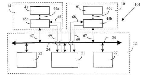
With reference to Figure 2, an electronic circuit 101
according to the invention is for instance formed by an
emulation subsystem of the type described in Figure 1,
wherein to the hardware block 41 and to the firmware block 61
are associated a first interface device (first device) 45a
and a second interface device 45b, situated between the
respective blocks 41 and 61, and BUS 24, respectively.
In particular, in agreement with the present example of
embodiment, the first module 14, formed for instance by the
ARM INTEGRATOR/LM module, includes a programmable logic
circuit of FPGA type (hardware block) 41, for instance type
XC200E by XILINK Corp., and the first device 45a.
The first device 45a is connected by means of a first
connection 46a to the hardware block 41, by means of a second
connection 47 to BUS 24 (Figures 2 and 3), incorporating as
known an ADDRESS BUS 24a, a CONTROL BUS 24b and a DATA BUS
24c, and by means of control wires 48 and 49 of a known type,
for instance, for the exchange of Interrupt I/0 signals with
the CPU 21.
The second module 61, formed for instance by a PCI
(Peripheral Component Interconnect) module of a known type,
includes a DSP microprocessor (firmware block) 61, for
instance TMS320C6201 by Texas Instruments Corp., and the
second device 45b.
The second device 45b is connected by means of a first
connection 46b to the firmware block 61, by means of a second
CA 02457880 2004-02-17
WO 03/019395 PCT/IT02/00549
6
connection 67 to the BUS 24 and by means of control wires 68
and 69 of a known type, to the CPU 21.
As will be explained in detail in the sequel, circuits 45a a
45b are designed to intercept determined control commands
(commands) coming from the CPU 21 and to control the transfer
of data from their respective blocks 41 and 61 to RAM 22, and
vice-versa, or from the hardware block 41 to the firmware
block 61, and vice-versa, without the control by CPU 21.
Obviously, as is easily understood by those skilled in the
art, the presence on circuit 101 of devices 45a and 45b, also
requires the presence of a control circuit (BUS arbiter) 27,
of a known type, designed to control the sequential acoess to
BUS 24 by CPU 21 and devices 45a and 45b.
Device 45a a 45b only differ by specialisation features
relating to the characteristics of the block to which they
are associated. Structure and functions of first device 45a
will be therefore described in the sequel.
Concerning the connections, as will be set forth hereinafter,
connections 46a and 46b are specific and bound to the
characteristics ~of respective blocks 41 and 61, whilst
connections 47, 48 and 49 and their corresponding 67, 68 and
~9 are of an equivalent type.
Device 45a comprises, for instance, a component capable
of controlling the data transfer (TRAMS CONTROLLER) 51, a
component for controlling the memory.(MEMORY CONTROLLER) 55,
and a block interface component (BLOCK CONTROLLER) 54a.
The TRAMS CONTROLLER 51 is connected to MEMORY CONTROLLER
55, BLOCK CONTROLLER 54a, ADDRESS BUS 24a and DATA BUS 24c,
and is designed to exchange commands with CPU 21, over
control wires 48 and 49, and to exchange data for instance
with RAM 22 by interacting with MEMORY CONTROLLER 55, or
collecting data from DATA BUS 24c, and transferring them to
BLOCK CONTROLLER 54a, or vice-versa.
CA 02457880 2004-02-17
WO 03/019395 PCT/IT02/00549
7
The TRAMS CONTROLLER 51 is also designed to exchange commands
with CPU 21 by means of DATA BUS 24c, in order to carry out,
for instance, initialisation functions or special functions
defined at the design stage of electronic circuit 101 and/or
device 45a, as will be described in detail later.
The TRAMS CONTROLLER 51 is formed, for instance, by a
state machine of a known type, capable of effecting a
sequence of predefined operations in connection with
predefined commands, such as Interrupt I/O signals coming
from CPU 21 or a partioular bit configuration present on DATA
BUS 24c during the initialisation stage.
In a preferred form of embodiment, the state machine of
TRAMS CONTROLLER 51 comprises, for instance, a memory for
storing programs (program memory) 511, and a sequences
circuit 512, both of a known type.
The program memory 511 serves, for instance, to store a
plurality of instruction sequences, developed at the design
stage, or defined at the configuration stage of the
electronic circuit 101.
The sequences circuit 512 is connected to the program memory
511 and is capable selectively reading and carrying out,
according to predefined commands coming from CPU 21, the
instruction sequences stored on the program memory 511.
Obviously, the different instruction sequences may be
implemented at the development or configuration stages of
electronic circuit 101, and are diversified, in a preferred
form of embodiment, into standard operation functions and
initialisation functions.
The MEMORY CONTROLLER 55 is connected to the TRAMS
CONTROLLER 51, ADDRESS BUS 24a and CONTROL BUS 24b, and has
the duty of requesting CONTROL BUS 24b, in a known manner, in
connection with commands coming from TRAMS CONTROLLER 51, to
activate read or write operations from or to an address of
CA 02457880 2004-02-17
WO 03/019395 PCT/IT02/00549
8
RAM 22, or an address of an additional circuit block on
ADDRESS BUS 24a, or on registers internal to MEMORY
CONTROLLER 55 itself.
For general use purposes, MEMORY CONTROLLER 55 comprises, for
instance, a MEMORY CONTROLLER GENERIC 551, capable of
generating a generic request function towards CONTROL BUS
24b, and an adaptation unit or MEMORY CONTROLLER SPECIFIC
552, capable of specialising the requests to CONTROL BUS 24b
as a function of the type of CONTROL BUS being used on the
electronic circuit 101.
The MEMORY CONTROLLER 55 may be implemented for instance
by using a discrete logic of a known type, or also, through
synthesis, starting from a memory controller belonging to a
library of components of said type and it will preferably
incorporate some registers to store addresses of RAM 22 to be
used for reading or writing data or addresses of additional
circuit blocks for a direct transfer of data.
Obviously, said addresses may be defined at the configuration
stage of device 45a, as a function of the characteristics of
the associated block 41, or predefined at the design stage of
the electronic circuit 101.
The BLOCK CONTROLLER 54a is connected to the hardware
block 41 and to the TRAMS CONTROLLER 51 and is designed to
control hardware block 41, on the basis of the commands
coming from the TRAMS CONTROLLER 51, in order that the
specific functions of the hardware block 41 are carried out.
The BLOCK CONTROLLER 54a has also the duty, upon
completion of the specific functions by hardware block 41, of
informing TRAMS CONTROLLER 51 about the completion of said
functions by the same block 41.
The BLOCK CONTROLLER 54a preferably comprises an I/O
BUFFER 541a, of a known type, for storing, in accordance with
CA 02457880 2004-02-17
WO 03/019395 PCT/IT02/00549
9
the present example of embodiment, data to be exchanged
between hardware block 41 and RAM 22, or another block.
In particular, I/O BUFFER 541a serves for instance to
alternatively store either data at the input of block 41 at
the time of activation of the same block, or data at the
output of block 41 upon completion of the functions of the
same block.
The BLOCK CONTROLLER 54a of the interface device 45a and
the BLOCK CONTROLLER of the interface device 45b are
specialised on the block to which they are associated, since
the activation characteristics of respective blocks (41 and
61) and the size of the data to be exchanged for each block
are generally diversified from block to block thus, devices
45a and 45b differ, in accordance with the present example of
embodiment, only by the characteristics of respective BLOCK
CONTROLLERs, which, as described before, depend in turn on
the characteristics of blocks 41 and 61 to which they are
interfaced.
The BLOCK CONTROLLERS may be implemented for, instance
through elementary logic circuits or also through state
machines having predefined functions in relation to commands
coming from the associated TRAMS CONTROLLER or respective
block 41 or 61.
Preferably, at the initialisation stage of electronic
circuit 101, the BLOCK CONTROLLERS are designed to be
programmed by CPU 21 by means of the associated TRAMS
CONTROLLER. Therefore by virtue of said characteristic they
are able to allow the adaptation of the characteristics of
respective blocks to those of the electronic circuit on which
they are placed.
By virtue of the described architecture and in agreement
with the present invention, device 45a associated to hardware
block 41 and device 45b associated to firmware block 61 are
CA 02457880 2004-02-17
WO 03/019395 PCT/IT02/00549
able to activate and perform the data transfer from RAM 22 to
respective blocks (41 and 61), and vice-versa, by greatly
reducing the load of CPU 21 and BUS 24.
Let us consider as an example the data transfer from the
5 hardware block 41 to the RAM 22.
In connection with the signalling by BLOCK CONTROLLER 54b of
the completion of the functions of hardware block 41, TRAMS
CONTROLLER 51 sends the request - without requiring CPU 21 to
intervene - to MEMORY CONTROLLER 55 to activate the writing
10 on RAM 22 of content of I/0 BUFFER 541a to the addresses
indicated on the registers inside MEMORY CONTROLLER 55.
Following the activation of write commands, the TRAMS
CONTROLLER 51 transfers the content of I/0 BUFFER 541a to the
RAM 22, and when said transfer has ended, it sends CPU 21
over wire 49 an Interrupt I/O signal to inform of transfer
completion.
As will be easily appreciated by those skilled in the
art, thanks to the present invention the data transfer from
hardware block 41 to RAM 22 does not require the intervention
of CPU 21 and occupies BUS 24 only once; thus allowing, all
conditions being equal, a reduction of CPU~21 load and by 50
0 of BUS 24 occupation, as compared to the state of the
art.
For the sake of completeness, the description also
includes an example relating to the determination of the
addresses of RAM 22 on which the data are to be stored.
Said operation may be carried out at a initialisation or
start up stage of the electronic circuit 101 by envisaging
for instance that over DATA BUS 24c during said stage 51 a
predefined command of initialisation is presented to the
TRAMS CONTROLLER 51 by the CPU 21 and that upon this
instruction the TRAMS CONTROLLER 51 reads from the ADDRESS
BUS 24c the addresses of RAM 22 to be used for read and write
CA 02457880 2004-02-17
WO 03/019395 PCT/IT02/00549
11
operations by the associated block and stores them into the
registers internal to the MEMORY CONTROLLER 55.
The operation of electronic circuit 101 described so far
is the following.
At the initialisation step, the CPU 21 configures all
the devices present on the electronic circuit, for instance
devices 45a and 45b, by sending specific commands to each
device, 45a or 45b, and presenting on the ADDRESS BUS 24a the
addresses of RAM 22 or of the blocks which each device must
use at the write and read phases for exchanging data in
operation.
During the operation phases, for instance, data reading
from RAM 22, the CPU 21 notifies, by means of Interrupt I/0
signals, to devices 45a or 45b that the data are available
for reading, in order that devices 45a or 45b may collect the
data from RAM 2'2, at the address defined at the
initialisation stage, and make them available to the
respective blocks 41 and 61, without any additional
intervention by CPU 21.
During the writing of data on RAM 22, for instance, the'
devices 45a or 45b engage BUS 24 and directly transfer the
data from respective blocks 41 or 61 to RAM,22 to the
addresses assigned at.the initialisation stage, and only upon
transfer completion they notify, by means of Tnterrupt I/0
signals, the end of the write operation to CPU 21.
Thanks to devices 45a and 45b, write and read operations
from and to RAM 22 are performed in such a way that
- CPU 21 only carries out the control functions of electronic
circuit 101 and does not look, for instance, to the specific
function of data transfer in the transmission chain;
- BUS 24 is not engaged by CPU 21 during the data transfer
operations; as a matter of fact, CPU 21 only acts on the
basis of Interrupt I/0 signals, and uses BUS 24 only in the
CA 02457880 2004-02-17
WO 03/019395 PCT/IT02/00549
12
event of initialisation commands or in the event of specific
control commands, such as, for instance, the emptying of the
output buffer of block 41 or 61, without extracting data from
RAM 22, etc.
In case of direct data transfer from a first block to a
second circuit block, the configuration of electronic
circuit 10l is such that devices associated to the blocks
contain write and read addresses corresponding to the devices
on which the read and write operations must be performed.
In this form of implementation, for instance, at the
initialisation stage CPU 21 sends to device 45a the address
of the I/O BUFFER of device 45b, for its storing on the
internal registers of the MEMORY COI~TROLhER 55.
During the operation phases, in connection with Interrupt I/0
signals coming from CPU 21, device 45a activates hardware
block 41 for carrying out the defined functions, and upon
completion of said functions, it directly transfers the
processed data to device 45b; only at the end of said
transfer, in accordance with such form of embodiment, device
45a informs, through Interrupt O/I signals, CPU 21 of the end
of block 41 activity and of the transfer.
As will become evident to those skilled in the art, this form
of embodiment reduces the occupation of BUS 24 and CPU 21 by
more than 50 0 ,as compared to the existing state of the art.
The description has been effected making reference to a
first device 41a, associated to a hardware block 41, and to a
second device 41b, associated to a firmware block 61, and the
data exchange between said blocks, but it will become evident
to those skilled in the art that the characteristics of the
invention remain unchanged in the case in which the devices
are associated to homogeneous blocks, for instance, all of
hardware type or firmware type, and the data exchange takes
place between homogeneous blocks.
CA 02457880 2004-02-17
WO 03/019395 PCT/IT02/00549
13
Devices 45a a 45b have been described as separate from
their respective circuit blocks 41 and 61 to which they are
associated. As will be clear to those skilled in the art,
device 45a may be for instance implemented by synthesis and
integrated into hardware block 41, being formed, as already
described, by circuit elements the models of which may be
easily retrieved from a library of components.
Likewise, device 45b, associated to firmware block 61,
may be implemented in the form of a firmware performing the
logic architecture of the described device, provided that, as
will become evident to those skilled in the art, the
microprocessor or DSP used as firmware block is capable of
being directly connected to BUS 24 and to control wires 68
and 69.
The present description has been made by associating a
respective device to each circuit block, but as will be clear
to those skilled in the art, said condition is strictly
required only to guarantee that each block may directly
transfer data to other blocks, without increasing the CPU and
BUS load.
Obvious modifications or variations are possible to the
above description, concerning size, dimensions, forms,
materials, components, circuit elements, connections and
contacts, as well as details of the circuitry and
~5 implementation presented herein, and of the method of
operation, without departing from the spirit and scope of the
invention, as defined by the appended claims.