Note: Descriptions are shown in the official language in which they were submitted.
CA 02458060 2004-02-18
WO 03/030009 PCT/US02/30240
1
PROGRAMMABLE GATE ARRAY HAVING INTERCONNECTING LOGIC TO
SUPPORT EMBEDDED FIXED LOGIC CIRCUITRY
TECHNICAL FIELD OF THE INVENTION
This invention relates generally to programmable gate
arrays and in particular to embedding fixed logic circuits
within such programmable gate arrays.
BACKGROUND OF THE INVENTION
Programmable devices are a class of general-purpose
integrated circuits that can be configured for a wide
variety of applications. Such programmable devices have
two basic versions, mask programmable devices, which are
programmed only by a manufacture, and field programmable
devices, which are programmable by the end user. In
addition, programmable devices can be further categorized
as programmable memory devices or programmable logic
devices. Programmable memory devices include programmable
2o read only memory (PROM), erasable programmable read only
memory (EPROM) and electronically erasable programmable
read only memory (EEPROM). Programmable logic devices
include programmable logic array (PLA) devices,
programmable array logic (PAL) devices, erasable
programmable logic devices (EPLD) devices, and programmable
gate arrays (PGA).
Field programmable gate arrays (FPGA) have become very
popular for telecommunication applications, Internet
applications, switching applications, routing applications,
and a variety of other end user applications. Figure 1
illustrates a generic schematic block diagram of a field
programmable gate array (FPGA) 10. The FPGA 10 includes
programmable logic fabric 12 (containing programmable logic
gates and programmable interconnects) and programmable
input/output blocks 14. The programmable input/output
blocks 14 are fabricated on a substrate supporting the FPGA
10 and are coupled to the pins of the integrated circuit,
allowing users to access the programmable logic fabric 12.
The programmable logic fabric 12 may be programmed to
CA 02458060 2004-02-18
WO 03/030009 PCT/US02/30240
2
perform a wide variety of functions corresponding to
particular end user applications. The programmable logic
fabric 12 may be implemented in a variety of ways. For
example, the programmable logic fabric 12 may be
implemented in a symmetric array configuration, a row-based
configuration, a column-based configuration, a sea-of-gates
configuration, or a hierarchical programmable logic device
configuration.
Figure 2 illustrates the programmable logic fabric 12
lo implemented in accordance with a symmetrical array
configuration. As shown, a plurality of logic blocks 16 is
configured as an array of rows and columns. Each of the
plurality of logic blocks 16 may be programmed by the end
user to perform a specific logic function. More complex
logic functions may be obtained by interconnecting
individually programmed logic blocks using a plurality of
programmable interconnections 18. Accordingly, between
each of the logic blocks of each row and each column are
programmable interconnections 18.
The programmable interconnections 18 provide the
selective connectivity between the logic blocks of the
array of logic blocks 16 as well as between the logic
blocks and the programmable input/output blocks 14. The
programmable interconnections 18 may be implemented using
any programmable element, including static RAM cell
technology, fuse and/or anti-fuse cell technologies, EPROM
transistor technology, and/or EEPROM transistor technology.
If the FPGA utilizes static RAM programmable connections,
the connections can be made using a variety of components,
including pass transistors, transmission gates, and/or
multiplexers that are controlled by the static RAM cells.
If the FPGA utilizes anti-fuse interconnections, the
interconnections typically reside in a high impedance state
and can be reprogrammed into a low impedance, or fused,
state to provide the selective connectivity. If the FPGA
utilizes EPROM or EEPROM based interconnections, the
interconnection cells may be reprogrammed, thus allowing
the FPGA to be reconfigured.
CA 02458060 2004-02-18
WO 03/030009 PCT/US02/30240
3
Figure 3 illustrates a schematic block diagram of the
programmable logic fabric 12 being implemented as a row
based configuration. In this configuration, the
programmable logic fabric 12 includes a plurality of logic
blocks 16 arranged in rows. Between each row of the logic
blocks are programmable interconnections 18. The
interconnections may be implementing utilizing any
programmable storage elements, including RAMs (static,
dynamic and NVRAM), fuse and/or anti-fuse technologies,
EPROM technology, and/or EEPROM technology.
Figure 4 illustrates a schematic block diagram of the
programmable logic fabric 12 being implemented as a column-
based configuration. Logic blocks 16 and programmable
interconnections 18 in Figures 3 and 4 are substantially
similar.
Figure 5 illustrates the programmable logic fabric 12
being implemented as a hierarchical programmable logic
device. In this implementation, the programmable logic
fabric 12 includes programmable logic device blocks 22 and
programmable interconnections 18. As shown, four
programmable logic block devices 22 are in the corners with
an interconnection block 18 in the middle of the logic
device blocks. In addition, the.interconnections include
lines coupling the programmable logic device blocks 22 to
the interconnection block 18.
As is known, field programmable gate arrays allow end
users the flexibility of implementing custom integrated
circuits while avoiding the initial cost, time delay and
inherent risk of application specific integrated circuits
(ASIC). While FPGAs have these advantages, there are some
disadvantages. For instance, an FPGA programmed to perform
a similar function as implemented in an ASIC can require
more die area than the ASIC. Further, the performance of a
design using a FPGA may in some cases be lower than that of
a design implemented using an ASIC.
One way to mitigate these disadvantages is to embed
into an FPGA certain commonly used complex functions as
fixed logic circuits. Therefore, a need exists for a
CA 02458060 2008-08-26
74842-43
4
programmable gate array that includes embedded fixed logic
circuits yet retains programmable components.
SUMMARY
In accordance with one particular aspect of the
invention, there is provided a programmable gate array
comprising: programmable logic fabric; a first fixed logic
circuit having at least one input and at least one output,
and the first fixed logic circuit is physically located
within the programmable logic fabric; and first
interconnecting logic operable to couple the at least one
input and the at least one output of the first fixed logic
circuit to the programmable logic fabric, the first
interfacing logic comprises a first switch matrix connected
to the at least one input of the first fixed logic circuit,
a second switch matrix connected to the at least one output
of the first fixed logic circuit, a first term tile
connected to the first switch matrix and a second term tile
connected to the second switch matrix.
BRIEF DESCRIPTION OF THE DRAWINGS
Figure 1 illustrates a schematic block diagram of
a prior art field programmable gate array;
Figure 2 illustrates a schematic block diagram of
the programmable logic fabric of the programmable gate array
of Figure 1 being implemented in a symmetrical array
configuration;
Figure 3 illustrates a schematic block diagram of
the programmable logic fabric of the programmable gate array
of Figure 1 being implemented as a row based configuration;
CA 02458060 2008-08-26
74842-43
Figure 4 illustrates a schematic block diagram of
a programmable logic fabric of the programmable gate array
of Figure 1 being implemented as a column based
configuration;
5 Figure 5 illustrates a schematic block diagram of
the programmable logic fabric of the programmable gate array
of Figure 1 being implemented as a hierarchical programmable
logic device configuration;
Figure 6 illustrates a graphical diagram of a
programmable gate array in accordance with an embodiment of
the present invention;
Figure 7 illustrates a graphical diagram of an
alternate programmable gate array in accordance with an
embodiment of the present invention;
Figure 8 illustrates a graphical diagram of
another programmable gate array in accordance with an
embodiment of the present invention;
Figure 9 illustrates a more detailed graphical
diagram of the programmable gate array of Figure 3;
Figures 10A illustrates a schematic block diagram
of the interconnecting tiles and interfacing logic in
accordance with an embodiment of the present invention;
Figure l0B illustrates a schematic block diagram
of the interconnecting tiles and an embodiment of the
interfacing logic in accordance with the present invention;
Figure 11 illustrates a schematic block diagram of
the interconnecting tiles interfacing with the programmable
CA 02458060 2008-08-26
74842-43
5a
logic fabric in accordance with an embodiment of the present
invention;
Figure 12 illustrates a graphical diagram of yet
another programmable gate array in accordance with an
embodiment of the present invention;
Figure 13 illustrates a graphical diagram of a
variation of the programmable gate array of Figure 12; and
Figure 14 illustrates a graphical diagram of a
further variation of the programmable gate array of
Figure 12.
DETAILED DESCRIPTION
Generally, some embodiments of the present
invention provide interconnecting logic that interfaces an
embedded fixed logic circuit, or circuits, with programmable
logic fabric of a programmable gate array. The
interconnecting logic enables any fixed logic circuit
(e.g., a digital signal processor, microprocessor, physical
layer interface, link layer interface, network layer
interface, audio processor, video graphics processor, and/or
applications specific integrated circuit) to be embedded
within the programmable logic fabric of a programmable gate
array. In addition, the interconnecting logic provides
connectivity between the fixed logic circuit and the
programmable logic fabric such that the fixed logic circuit
can be connected to any other blocks in the programmable
logic fabric.
The interconnecting logic includes interconnecting
tiles and may further include interfacing logic. The
interconnecting tiles provide programmable connectivity
between inputs and/or outputs of the fixed logic circuit and
CA 02458060 2008-08-26
74842-43
5b
the interconnects of the programmable logic fabric. The
interfacing logic, when included, conditions signals between
the fixed logic circuit and the programmable logic fabric.
The signal conditioning can include data format changes,
parallel-to-serial conversion, serial-to-parallel
conversion, multiplexing, demultiplexing, performing logic
functions and/or control signal generation, etc. With such
interconnecting logic, any fixed logic circuit may be
CA 02458060 2004-02-18
WO 03/030009 PCT/US02/30240
6
readily embedded within a programmable gate array to
provide additional functionality to the end users of FPGAs.
The present invention can be more fully described with
reference to Figures 6 through 18. Figure 6 illustrates a
block diagram of a programmable gate array 30. The
programmable gate array may be a field programmable gate
array or a mask programmable gate array. In addition, the
programmable gate array may include programmable logic
device functionality, programmable array logic
functionality, programmable logic arrays, et cetera. The
programmable gate array 30 includes the programmable logic
fabric 12, the programmable input/output blocks 14,
interconnecting logic 34, and a fixed logic circuit 32.
The fixed logic circuit 32, which may include any
logic function, such as a digital signal processor,
microprocessor, physical layer interface, link layer
interface, network layer interface, network processor,
audio processor, video graphics processor, logic circuitry,
and/or application specific integrated circuits, includes
at least one input and at least one output. Typically, the
fixed logic circuit 32 includes a plurality of inputs and a
plurality of outputs, which are represented by input/output
ports 36, 38, 40 and 42. The input/output ports 36-42 are
operably coupled to the interconnecting logic 34, which
provides connectivity between the input/output ports of the
fixed logic circuit 32 and the programmable logic fabric 12
of the programmable gate array 30, as well as between the
various logic functions in the interconnecting logic. It
should be noted that more than one fixed logic circuit can
3o be included in the programmable gate array 30.
The programmable logic fabric 12 includes a plurality
of configurable logic blocks (CLB's) and programmable
interconnects. The architecture of the programmable logic
fabric may be row or column based, hierarchical-PLD,
symmetrical array, and/or a sea of gates. The configurable
logic blocks may be of the type found in the XC4000E family
of FPGAs, Virtex and/or the Virtex-II FPGAs manufactured
and distributed by Xilinx, Inc. The interconnects may
include a plurality of programmable switch matrices that
CA 02458060 2004-02-18
WO 03/030009 PCT/US02/30240
7
utilize static RAM cell technology, fuse and/or anti-fuse
cell technologies, EPROM transistor technology, EEPROM
transistor technology and/or any other programmable
technology. The switch matrices may be of the type found
in the XC4000E family of FPGAs, Virtex and/or the Virtex-II
FPGAs manufactured and distributed by Xilinx, Inc. The
programmable I/0 blocks 14 may be of the type found in the
XC4000E family of FPGAs, Virtex and/or the Virtex-II FPGAs
designed and manufactured by Xilinx, Inc.
The programmable gate array 30 may be implemented as
an integrated circuit. In one embodiment, the circuitry of
each of these elements 12, 14, 32 and 34, are implemented
using CMOS technology on a silicon substrate. However, as
one of average skill in the art will appreciate, other
integrated circuit technologies and substrate compositions
may be used.
In operation, the interconnecting logic 34 provides
coupling between the programmable logic fabric 12 and the
fixed logic circuit 32. As such, end users of the
programmable gate array 30 may program the PGA 30 treating
the fixed logic circuit 32 as a component of the
programmable logic fabric 12. For example, if the fixed
logic circuit 32 is a microprocessor, the interconnecting,
logic 34 might include memory for storing programming
25,instructions and/or data for the microprocessor and may
further include logic functions (e.g., memory controller)
to interface with other blocks of the PGA 30. Accordingly,
the programmable logic fabric 12 is programmed to perform
desired functions in combination with the fixed logic
functions of the microprocessor. Thus, with an embedded
microprocessor, the programmable gate array 30 offers the
flexibility of a FPGA with the processing efficiency of a
custom designed microprocessor. In addition, by embedding
a microprocessor within the programmable logic fabric, as
opposed to having two separate integrated circuits (one for
the microprocessor and another for the FPGA), power
consumption is reduced and performance increased due to the
elimination of interconnecting pins and traces between the
two separate integrated circuits. Other advantages include
CA 02458060 2004-02-18
WO 03/030009 PCT/US02/30240
8
easier implementation of multi-processor designs and
support for a wider range of system level designs (e.g.,
processor systems with no external memory). Further, the
programmable gate array 30 requires less printed circuit
board real estate than separate integrated circuits for an
FPGA and a microprocessor.
Figure 7 illustrates a graphical diagram of an
alternate programmable gate array 50. The programmable
gate array 50 includes the programmable logic fabric 12,
so the programmable input/output blocks 14, a lst fixed logic
circuit 32, lst interconnecting logic 34, a 2 d fixed logic
circuit 52 and 2 d interconnecting logic 54. In this
illustration, the interconnecting logic 34 and fixed logic
circuit 32 are as generally described with reference to
Figure 6.
The 2nd fixed logic circuit 52 may include any logic
functions, such as a digital signal processor,
microprocessor, physical layer interface, link layer
interface, network layer interface, audio processor, video
graphics processor, logic circuitry, and/or an application
specific integrated circuit. The 2 d fixed logic circuit 52
includes a plurality of input/output ports 56, 58, 60 and
62 that allow it to interface with the 2d interconnecting
logic 54. The 2d interconnecting logic 54 provides the
connectivity between the 2a fixed logic circuit 52 and the
programmable logic fabric 12.
Figure 8 illustrates a graphical diagram of another
programmable gate array 70. The programmable gate array 70
includes the programmable logic fabric 12, the programmable
input/output blocks 14, and four fixed logic circuits 32,
52, 72 and 76. The structure of each fixed logic circuit
is similar to the fixed logic circuit shown in Fig. 7 (note
that the I/Os in each fixed logic circuit are not shown
because of the limited size of the drawings). Each fixed
logic circuit 32, 52, 72 and 76 has its own corresponding
interconnecting logic.34, 54, 74 and 78, respectively. The
interconnecting logic 34, 54, 74 and 78 provide its
respective fixed logic circuit connectivity to the
programmable logic fabric 12.
CA 02458060 2004-02-18
WO 03/030009 PCT/US02/30240
9
The construct of interconnecting logic 34, 54, 74 and
78 will be dependent upon the type of fixed logic circuit
it is supporting. For instance, if the fixed logic circuit
is a simple fixed logic function, such as a state machine
or a combinational logic circuit to perform a particular
logic function, the interconnecting logic 34, 54, 74 and/or
78 would include interconnecting tiles. The '
interconnecting tiles will be described in greater detail
with reference to Figures 9 through 11. If, however, the
lo fixed logic circuit is more complex, such as a digital
signal processor, microprocessor, physical layer interface,
link layer interface, network layer interface, audio
processor, video graphics processor, network processor,
and/or applications specific integrated circuit, the
interconnecting logic 34, 54, 74 and/or 78 may include a
plurality of interconnecting tiles and (optionally)
interfacing logic. The interfacing logic will be described
in greater detail with reference to Figures 9 and 10.
Figure 9 illustrates a more detailed graphical diagram
of a portion of the programmable gate array 30 of Figure 6.
While Figure 9 is illustrated with reference to the PGA 30
of Figure 6, the concepts regarding the interconnecting
logic 34 are equally applicable to the interconnecting
logic 54 of Figure 7, and the interconnecting logic 54, 74,
and 78 of Figure 8. As one of average skill in the art
will appreciate, any number of fixed logic circuits may be
embedded within the programmable logic fabric using
interconnecting logic.
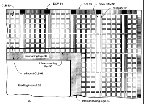
As shown in Figure 9, the programmable logic fabric 12
includes a plurality of configurable logic blocks (CLB) 80,
a plurality of memory blocks (Block RAM) 90, and a
plurality of multipliers 92. The programmable I/0 block
section 14 includes a plurality of individual I/0 blocks
(IOB) 86 and a plurality of digital clock managers (DCM)
84. The operations of the configurable logic blocks 80,
the digital clock managers 84, the input/output blocks 86,
the block RAM 90, and the multipliers 92 function in a
similar manner as corresponding components found in the
XC4000E family of field programmable gate arrays, Virtex
CA 02458060 2004-02-18
WO 03/030009 PCT/US02/30240
and/or the Virtex-II field programmable gate arrays
designed and manufactured by Xilinx, Inc.
As shown, the configurable logic blocks 80, the block
RAM 90 and the multipliers 92 are arranged in a series of
5 rows and columns. The fixed logic circuit 32 displaces
some of the components in programmable logic fabric 12
while at the same time is able to integrate with the
remaining components in the programmable logic fabric. With
some of the programmable logic fabric displaced, regular
10 operation of the FPGA would be interrupted. This
interruption occurs as a result of discontinuity of
connectivity between the plurality of configurable logic
blocks 80, the block RAMs 90, and multipliers 92. One
aspect of the present invention is an architecture that
allows for full integration of the fixed logic circuit 32
into the programmable logic fabric 12 without discontinuity
of connectivity.
In the FPGA 30, each CLB 80, IOB 86, block RAM 90, and
multiplier 92 is associated with at least one of the
plurality of programmable switch matrices. The plurality
of programmable switch matrices provides selective
connectivity throughout the programmable logic fabric.
With the.insertion of the fixed logic circuit 32 and
interconnecting logic 34, the connectivity pattern of the
programmable logic fabric is interrupted. The present
invention uses a plurality of interconnecting tiles 96 to
provide programmable connectivity between (a) the
interfacing logic 94, when included, and the fixed logic
circuit 32 and (b) the plurality of CLBs 80, block RAM's 90
and/or multipliers 92 of the programmable logic fabric 12.
The intetconnecting tiles 96 will be discussed in greater
detail with reference to Figure 11.
The interfacing logic 94 conditions signal transfers
between the fixed logic 32 and the CLBs 80, block RAM 90
and/or multipliers 92 of the programmable logic fabric 12.
Such conditioning is dependent upon the functionality of
the fixed logic circuit 32. For example, if the fixed
logic circuit 32 processes video and/or audio signals in
the analog domain, the interfacing logic 94 could include
CA 02458060 2004-02-18
WO 03/030009 PCT/US02/30240
11
analog to digital converters and digital to analog
converters. If the fixed logic circuit 32 is a
microprocessor, the interfacing logic generates and
conditions the signals for interfacing the FPGA with the
microprocessor (e.g., address buses, data buses and/or
control signals of the microprocessor, and FPGA control
signals for various modes of operations, such as power-up
and configuration). The interfacing logic 94 may include
test circuitry for testing the embedded fixed logic circuit
lo and the surrounding programmable logic fabric. In addition,
hard peripherals of the microprocessor may also be included
in the interfacing logic.
Figure l0A illustrates a schematic block diagram of a
microprocessor 100 being embedded in the FPGA 30 as an
example of a fixed logic circuit. It should be noted that
the present invention is applicable to processors of any
design, and is not limited to a particular type of
processor. As one of average skill in the art will
appreciate, the physical design of the microprocessor 100
can have a variety of geometric configurations. The
microprocessor 100 is surrounded by the interconnecting
logic 34 (shown in Fig. 9) that includes the interfacing
logic 94 and a plurality of interconnecting tiles 96. The
microprocessor 100 may be connected to block RAMs 96
through memory controllers (not shown). The microprocessor
100 may be directly connected to the block RAMs 90. By
providing coupling between the microprocessor 100 and the
block RAMs 90, the block RAMs 90 may be shared by the
microprocessor 100 and the programmable logic fabric 12.
Such direct sharing eliminates the need for programming the
programmable logic fabric to provide the microprocessor
with access to the RAMs 90.
The interface logic 94 may contain one or more blocks
of logic gates. These blocks may be designed to perform any
logic function, and may communicate in any manner with the
microprocessor 100, the block RAMs 90, and the
interconnecting tiles 96. In Fig. 10A, only one such block
(114) of logic functions is shown. The interface logic 94
may also contain one or more blocks of configurable logic
CA 02458060 2004-02-18
WO 03/030009 PCT/US02/30240
12
gates. These blocks may be configured to perform any logic
function, and may communicate in any manner with the
microprocessor 100, the block RAMs 90, and the
interconnecting tiles 96. In Fig. 10A, only one such block
(116) of configurable logic functions is shown. The
interface logic 94 may further contain a test module 103
that, controls the manufacturing testing of the
microprocessor 100, interconnecting tiles 96, and/or
various parts of the interfacing logic 94. In Fig. 10A,
even though the test module 103 is shown as an isolated
block to simplify the diagram, in reality it will be
connected to some or all of the above mentioned components.
A control module 105 can be used to control the operations
of the microprocessor 100 and various components in the
interfacing logic 94. The interface logic 94 may also
contain a timing module 107 that generates various timing
signals for the microprocessor 100 and other components in
the interface logic 94. The timing module 107 may contain
clock generation circuits (such as oscillators), or may use
some of the clock signals of the programmable logic fabric.
In Fig. 10A, even though the control module 105 and timing
module 107 are shown as isolated blocks, they are in
reality connected to some or all of the above mentioned
components. In addition, modules performing other functions
may also be included.
The microprocessor 100 may communicate directly with
the interfacing tiles 96 (which are programmably connected
to the CLBs 98 shown in Fig. 9). The microprocessor 100 may
also communicate with the interfacing tiles 96 through the
3o blocks of logic gates 114 and blocks of programmable logic
gates 116. The connections-shown in Figure 10A could be
unidirectional and/or bidirectional.
The block RAM 90 may store at least a portion of the
executable instruction code for the microprocessor 100. In
addition, such memory may store the data to be processed by
the microprocessor 100 and the data already processed by
the microprocessor 100. Because the memory is shared
between the microprocessor 100 and the programmable logic
fabric 12, configured portions of the programmable logic
CA 02458060 2004-02-18
WO 03/030009 PCT/US02/30240
13
fabric 12 may retrieve the data to be processed and/or the
data already processed to perform a certain function upon
the data.
It should be noted that the block RAM 90 may be at any
position relative to the microprocessor 100 (top, down,
left or right).
A specific implementation of an interface logic is
shown in Figure 10B. To efficiently input and output
signals from microprocessor 100, which may include more
than nine hundred input and/output connections, the
interfacing logic 94 includes a plurality of multiplexers
118, 128, 132, 136, 142, 146, and 150 and/or a plurality of
demultiplexers 120, 130, 134, 138, 140, 144, and 148. The
multiplexers 118, 128, 132, 136 142, 146, and 150 function
to transmit two or more signals over a single path, to
serialize parallel data, and/or to select one of multiple
input signals. The demultiplexers 120, 130, 134, 138, 140,
144, and 148 function to separate multiple signals on one
path into separate signals on multiple paths or to convert
serial data into parallel data. It should be noted that
multiplexers/demultiplexers may have inputs and outputs of
multiple signal widths (i.e., the output of a multiplexer
may have more than one signal and the input of a
demultiplexer may have more than one signal).
As shown, demultiplexer 134 facilitates reading data
and/or instructions from memory 108. Memory 108 may be
single or multi port memory. For example, demultiplexer 134
receives a serial stream of data from memory 108 and
provides it in parallel to an address bus interface, data
3o bus interface, and/or an instruction bus interface of the
microprocessor 100. Multiplexer 132 facilitates writing
data to memory 108. In this example, multiplexer 132
receives parallel data from the microprocessor 100 and
converts the parallel data into serial data for storing in
memory 108. As one of average skill in the art will
appreciate, the microprocessor 100 may also have one or
more direct connections to memory 108 exclusive of the
multiplexer 132 and demultiplexer 134 or in combination
therewith. As one of average skill in the art will further
CA 02458060 2004-02-18
WO 03/030009 PCT/US02/30240
14
appreciate, the microprocessor 100 may have more or less
multiplexers and demultiplexers coupling it to memory 108.
Multiplexer 128 provides multiplexing of multiple
signals from the BRAM 90 to the left of the microprocessor
100 into a single stream of data to memory 108. As such,
data and/or instructions from the BRAM 90 may be delivered
to the microprocessor 100. Demultiplexer 130 provides
demultiplexing of a single stream of data from memory 108
in to a plurality of separate signals, which are coupled to
BRAM 90. As such, the microprocessor 100 may write data to
the BRAM 90 via memory 108. As one of average skill in the
art will appreciate, multiplexer 128 may include direct
coupling to the microprocessor 100, such that data being
retrieved from BRAM 90 does not have to be intermediately
stored in memory 108. As one of average skill in the art
will further appreciate, demultiplexer 130 may be directly
coupled to the microprocessor 100 such that data may be
directly written to the BRAM 90. As one of average skill
in the art will also appreciate, the microprocessor 100 may
2o have a direct connection to the BRAM 90 or through a memory
controller.
It should be noted that memory 108 may be connected to
the microprocessor 100 without the use of multiplexer 132
and demultiplexer 134. It should also be noted that memory
108 may be of any width (generally up to the width of the
microprocessor 100). Further, memory 108 may be used for
storing instructions, data or a combination of both.
Multiplexers 136 and 142 and demultiplexers 138 and
140 provide the microprocessor 100 with similar access to
memory 122 and the BRAM 90 on the right of the
microprocessor 100 as multiplexers 128 and 132 and
demultiplexers'130 and 134 provided the microprocessor 100
access to memory 108 and the BRAM 90 on the left. As one
of average skill in the art will appreciate, the
interconnecting logic 94 may include more are less memory
than the memory shown (i.e., memory 108 and memory 122) and
that such memory may be of any size to support the
microprocessor. In addition, the memory 108 and 122 may be
CA 02458060 2004-02-18
WO 03/030009 PCT/US02/30240
static RAM, dynamic RAM, and/or erasable programmable read
only memory.
As further shown in Figure 10B, Multiplexer 146
provides a direct connection between the microprocessor 100
5 and one of the plurality of interconnecting tiles 96 on the
left side of the microprocessor 100. As coupled,
multiplexer 146 receives parallel data and/or a plurality
of signals from a plurality of pins of the microprocessor
100. Depending on the functionality of multiplexer 146, it
lo can either select one of the plurality of signals to pass
to the interconnecting tile 96 and/or multiplex the
plurality of signals into a single signal. Multiplexer 150
provides similar connectivity between the microprocessor
100 and an interconnecting tile 96 on the right of the
15 microprocessor. As one of average skill in the art will
appreciate, the interconnecting logic 94 may include more
or less multiplexers like multiplexer 146 and multiplexer
150 on any side of the microprocessor 100, depending on the
desired connectivity to the microprocessor 100, the type of
microprocessor 100, and/or the size of the microprocessor
100.
Demultiplexer 144 provides a direct connection between
the microprocessor 100 and one of the plurality of
interconnecting tiles 96 on the left side of the
microprocessor 100. As coupled, demultiplexer 144 receives
serial data and/or a plurality of multiplexed signals from
at least one of the plurality of interconnecting tiles 96.
Depending on the functionality of demultiplexer 144, it
either converts the plurality of multiplexed signals into a
plurality of signals carried on separate paths or converts
the serial signal stream into parallel signals.
Demultiplexer 148 provides similar connectivity between the
microprocessor 100 and an interconnecting tile 96 on the
right of the microprocessor. As one of average skill in
the art will appreciate, the interconnecting logic 94 may
include more or less demultiplexers like demultiplexer 144
and demultiplexer 148, depending on the desired
connectivity to the microprocessor 100, the type of
CA 02458060 2004-02-18
WO 03/030009 PCT/US02/30240
16
microprocessor 100, and/or the size of the microprocessor
100.
The interfacing logic 94 may further include direct
connections between the microprocessor 100 and one or more
of the interconnecting tiles 96. Such direct connections
may be unidirectional communication paths for inputting
signals into the microprocessor 100 or for outputting
signals from the microprocessor 100. In addition, such
direct connections may be bidirectional communication paths
lo for inputting and outputting signals from the
microprocessor 100. Such direct connections are shown
coupled to the lower left and lower right portions of the
microprocessor 100. As one of average skill in the art
will appreciate, more or less direct connections may be
provided between the interconnecting tiles 96 and the
microprocessor 100 than those shown in Figure 10B (from any
side of the microprocessor 100).
The interfacing logic 94 may further include a test
module 102. The test module 102 is selectively coupled to
2o a plurality of interconnecting tiles 96 and to the
plurality of circuits within the interfacing logic 94.
(Such connections are not shown for clarity purposes.) In
general, the test module 102 controls the manufacturing
testing of the microprocessor, the interface logic and/or
the surrounding programmable logic fabric.
The interfacing logic 94 may further include a control
module 104, which is operably coupled to a plurality of
multiplexers 118 and 126 and demultiplexers 124 and 120.
The multiplexers 118 and 126 function to transmit two or
more control signals over a single path, to serialize
parallel control data, and/or to select one of multiple
control signals. The demultiplexers 120 and 124 function
to separate multiple control signals on one path in to
separate control signals on multiple paths or to convert
serial control signals into parallel control signals:
Multiplexers 118 and 126 and demultiplexers 120 and 124 are
operably coupled to a plurality of interconnecting tiles
96. As coupled, control signals can be inputted to the
control module 104 or outputted from the control module 104
CA 02458060 2004-02-18
WO 03/030009 PCT/US02/30240
17
via the interconnecting tiles 96 to the programmable logic
fabric and/or the IOBs 86 and between the control module
104 and the microprocessor 100. It should be noted that the
control module 104 may have direct connections to the
microprocessor 100 without any mult'iplexers/
demultiplexers.
In this illustration, the control module 104 is
operably coupled to the microprocessor 100, which is
essentially a microprocessor core. In general, the control
module 104 provides control signals that control the
operations of the microprocessor 100 and receive related
control information from the microprocessor 100. For
example, the control module 104 may provide control
functions for interrupts, clocks, resets, power management,
instruction cache control, data cache control, direct
memory access (DMA) control, RAM memory control, external
peripheral bus control, UART control, and/or general
purpose I/0 control. Such control functions of a
microprocessor are known, thus no further discussion will
2o be presented except to enhance the understanding of the
present invention.
The interfacing logic 94 may further include a timing
module 106 that includes timing circuits. The timing
circuits can perform such functions as generating 64-bit
time-based timers, programmable interval timers, fixed
interval timers, and watchdog timers. In addition, the
timing module may provide clock signals to the configurable
logic gates 116 and/or the logic gate 114 (shown in Figure
10A) to latch data into and out of the circuits. Still
further, the timing module 106 may provide the timing to
latch data into and out of each of the multiplexers,
demultiplexers, and interconnecting tiles 96. The timing
module 106 may also obtain inputs (e.g. tick counter) from
and send outputs to the interconnecting tiles 96. The
functionality of timing circuits and debug modules used in
conjunction with a microprocessor 100 is known, thus no
further discussion will be presented except to further
illustrate the concepts of the present invention. As
mentioned in Figure 10A, the timing module may be connected
CA 02458060 2004-02-18
WO 03/030009 PCT/US02/30240
18
to all the components in the interfacing logic 94 and the
microprocessor 100.
As one of average skill in the art will further
appreciate, the interfacing logic 94 conditions signal
transfers between the fixed logic device 32, in this
example microprocessor 100, and the surrounding
programmable logic fabric 12, which includes the CLBs 80,
block RAM 90, and multipliers 92. Accordingly, the
interfacing logic 94 can perform a variety of logical
lo functions, including providing multiplexing of signals into
and/or out of the microprocessor, performing logic
functions upon input and/or output signals, storing the
signals, and providing direct coupling between the
programmable logic fabric and the microprocessor 100. In
addition, the interfacing logic 94 includes testing
functionality.
As one of average skill in the art will still further
appreciate, the circuitry embodying the interfacing logic
94 of Figure 10B represents one of an almost endless
combination of circuits that could comprise the interfacing
logic 94. As such, the interfacing logic 94 may include
more or less circuitry than that depicted in Figure 10B.
For example, the interfacing logic 94 may further include
analog to digital converters, digital to analog converters,
analog filters, digital filters, arithmetic logic units,
floating point units, interrupt controllers, memory
controllers, and/or memory management blocks.
As one of average skill in the art will also further
appreciate, while Figure 10B illustrates a microprocessor
100 as the embedded fixed logic circuit, the same concept
of interfacing logic 94 and a plurality of interconnecting
tiles 96 applies for any fixed logic circuit. For example,
the microprocessor 100 may be replaced with a digital
signal processor, video graphics processor, audio
processor, network processor, physical layer interface,
link layer interface, and/or network layer interface.
Depending on which type of fixed logic circuit is used, the
interfacing logic 94 may include more or less circuitry
than that shown in Figure 10B, but its function is the
CA 02458060 2004-02-18
WO 03/030009 PCT/US02/30240
19
same: condition signals transfers between the fixed logic
circuit and the programmable logic fabric.
Figure 11 illustrates a schematic block diagram of a
few of the interconnecting tiles 96-1 through 96-6 operably
coupling to the surrounding programmable logic fabric. The
surrounding programmable logic fabric includes a plurality
of configurable logic elements (CLE) 80-1 through 80-13 and
corresponding programmable switch matrices 154 through 188.
Solid lines between the programmable switch matrices
lo represent various interconnect lines that provide
connectivity in the programmable logic fabric. Dashed lines
in Figure 11 are provided to help visualization of the
geometry. An example of a FPGA architecture that can be
used in the present invention can be found in a U.S. patent
(Pat. No. 5,914,616) entitled "FPGA Repeatable Interconnect
Structure with Hierarchical Interconnect Lines."
Each interconnecting tile contains a programmable
switch matrix that is programmably connected to (a) a
programmable switch matrix in the programmable logic
fabric, (b) a termination tile (called herein "term tile"),
and (c) adjacent interconnecting tiles. Figure 11 shows six
matrices labeled 96-1-s to 96-6-s in the interconnecting
tiles 96-1 to 96-6, respectively. As an example, the
switch matrix 96-2-s is connected to the switch matrix 156
in the programmable logic fabric, a term tile T2, and
adjacent interconnecting tiles 96-1-s and 96-3-s.
Similarly, the switch matrix 96-5-s is connected to the
switch matrix 168 in the programmable logic fabric, a term
tile T4, and adjacent interconnecting tiles 96-4-s and 96-
3o 6-s. The six programmable switch matrices 96-1-s to 96-6-s
each contains a plurality of connections (shown as lines
151-1 to 151-6, respectively) that are connected to the
microprocessor 100 and/or components in the interfacing
logic 94.
The structure of switch matrices 96-1-s to 96-6-s is
substantially the same as that of the switch matrices in
the programmable logic fabric..
The function of the term tiles is to terminate the
interconnect lines and/or provide connectivity to the lines
CA 02458060 2004-02-18
WO 03/030009 PCT/US02/30240
that are interrupted by the microprocessor 100 and/or
components of the interfacing logic 94. In one embodiment
(e.g., the FPGA described in the above mentioned Pat No.
5,914,616), the programmable logic fabric contains single,
5 hex and long lines. In the term tiles, the single lines are
U-turned to other singles, the hex lines are rebuffered and
span to the far side of the microprocessor 100, and the
long lines span the microprocessor 100.
Figure 12 illustrates a schematic block diagram of an
10 alternate programmable gate array 230. The programmable
gate array 230 includes the programmable logic fabric 12,
the programmable input/output blocks 14, a fixed processing
module 234, 2nd interconnecting logic 238, another fixed
logic module (such as a high speed data interface 232) and
15 ls` interconnecting logic 236. The lst and 2nd
interconnecting logic 236 and 238 may include interfacing
logic and interconnecting tiles as previously described.
The high-speed data interface 232 may be a network layer
interface, such as TCP/IP interface, a physical layer
20 interface, such as Ethernet or asynchronous transfer mode
(ATM) interface, or a link layer interface. The fixed
processing module 234 may be a digital signal processor,
network processor, microprocessor, and/or microcomputer,
such that the programmable gate array provides a high-speed
data interface, a fixed processor and programmable logic
for a wide variety of telecommunication, networking, and/or
computing applications.
Figure 13 illustrates a variation of the gate array
230 of Figure 12. In Figure 13, the gate array 240 has the
high-speed data interface 232 positioned adjacent to the
programmable input/output blocks 14. As such, the high-
speed data interface 232 directly couples to at least some
of the programmable input/output blocks 14. In this
configuration, the lst interconnecting logic 232 partially
encircles the high-speed data interface 232.
Figure 14 illustrates a further variation of a
programmable gate array 250 that includes a high-speed data
interface 232 and a fixed processing module 234. In this
embodiment, the high-speed data interface is positioned in
CA 02458060 2004-02-18
WO 03/030009 PCT/US02/30240
21
a corner of the programmable gate array. As such, the
high-speed data interface 232 has direct access on 2 sides
to the programmable input/output blocks 14. As such, the
lst interconnecting logic 236 interfaces with 2 sides of the
high speed data interface.
From Figures 12-14, it should be clear to a person of
average skill in the art that a programmable gate array may
have any number and types of fixed logic modules positioned
at various locations interacting with each other in two-
sided, three-sided or four-sided configuration.
The preceding discussion has presented a programmable gate
array that includes interconnecting logic such that any
fixed logic circuit may be embedded within the programmable
logic fabric. Accordingly, the applications and
versatility of such a programmable gate array is
dramatically enhanced via the use of the present invention.
As one of average skill in the art will appreciate, other
embodiments may be derived from the teaching of the present
invention without deviating from the scope of the claims.