Note: Descriptions are shown in the official language in which they were submitted.
CA 02458440 2004-02-23
WO 03/019240 PCT/US02/26858
TITLE OF THE INVENTION
[0001] Optical Communications Systems, Devices, and
Methods
BACKGROUND OF THE INVENTION
[0002] The present invention is directed generally to the
transmission of signals in optical communications systems.
More particularly, the invention relates to systems, devices,
and methods for producing upconverted modulated optical
signals.
[0003] The development of digital technology provided the
ability to store and process vast amounts of information.
While this development greatly increased information
processing capabilities, it was recognized that in order to
make effective use of information resources it was necessary
to interconnect and allow communication between information
resources. Efficient access to information resources
requires the continued development of information
transmission systems to facilitate the sharing of information
between resources. One effort to achieve higher transmission
capacities has focused on the development of optical
transmission systems. Optical transmission systems can
provide high capacity, low cost, low error rate transmission
of information over long distances.
[0004] The transmission of information over optical
systems is typically performed by imparting the information
in some manner onto an optical carrier by varying
characteristics of the optical carrier. In most optical
transmission systems, the information is imparted by using an
information data stream to either directly or externally
modulate an optical carrier so that the information is
imparted at the carrier frequency or on one or more
sidebands, with the later technique sometimes called
upconversion or sub-carrier modulation ("SCM").
[0005] SCM techniques, such as those described in U.S.
Patent Nos. 4,989,200, 5,432,632, and 5,596,436, generally
1
CA 02458440 2004-02-23
WO 03/019240 PCT/US02/26858
produce a modulated optical signal in the form of two mirror
image sidebands at wavelengths symmetrically disposed around
the carrier wavelength. Generally, only one of the mirror
images is required to carry the signal and the other image is
a source of signal noise that also consumes wavelength
bandwidth that would normally be available to carry
information. Similarly, the carrier wavelength, which does
not carry information in an SCM system, can be a source of
noise that interferes with the subcarrier signal. Modified
SCM techniques have been developed to eliminate one of the
mirror images and the carrier wavelength. However,
"traditional" SCM techniques do not work well at high bit
rates (e.g., greater than 2.5 gigabits per second). For
example, mixer linearity, frequency flatness, frequency
bandwidth, and group delay tend to be problematic. It is also
difficult to keep power levels balanced and well controlled.
Such problems and difficulties can result in significant
performance degradation and/or increased cost. Modified SCM
techniques have also been disclosed to utilize Manchester
encoding in place of electrical carriers, such as described
in U.S. Patent Nos. 5,101,450 and 5,301,058.
[0006] Initially, single wavelength carriers were
spatially separated by placing each carrier on a different
fiber to provide space division multiplexing ("SDM") of the
information in optical systems. As the demand for capacity
grew, increasing numbers of information data streams were
spaced in time, or time division multiplexed ("TDM"), on the
single wavelength carrier in the SDM system as a means to
better use the available bandwidth. The continued growth in
demand has spawned the use of multiple wavelength carriers on
a single fiber using wavelength division multiplexing
( "WDM" ) .
[0007] In WDM systems, further increases in transmission
capacity can be achieved not only by increasing the
transmission rate of the information on each wavelength, but
also by increasing the number of wavelengths, or channel
count, in the system. However, conventional systems already
2
CA 02458440 2004-02-23
WO 03/019240 PCT/US02/26858
have the capacity to transmit hundreds of channels on a
single fiber, and that number will continue to increase. As
such, the cost of transmitters, receivers, and other devices
can constitute a large portion of a system's cost. Therefore,
the size and cost of systems will increase significantly as
the number of WDM channels increase. Accordingly, there is a
need to reduce the cost and size of devices in optical
systems while at the same time maintaining or increasing
system performance.
BRIEF SUMMARY OF THE INVENTION
[0008] The systems, devices, and methods of the present
invention address the above-stated need for lower cost,
higher capacity, longer distance optical communications
systems, devices, and methods. The present invention is
directed to improved systems, devices, and methods for
producing sub-carrier modulated optical signals. The present
invention can be employed, for example, in multi-dimensional
optical networks, point to point optical networks, or other
devices or systems which can benefit from the improved
performance afforded by the present invention.
[0009] One embodiment of the present invention is a
transmitter including an optical carrier source, an
electrical to optical converter, a parser, and first and
second Manchester encoders. The electrical to optical
converter has an optical input connected to the optical
carrier source, an optical output, and first and second
electrical data inputs. The parser has a data input and first
and second data outputs. The first Manchester encoder has a
data input connected to the first data output of the parser
and an encoded data output connected to the first electrical
input of the electrical to optical converter. The second
Manchester encoder has a data input connected to the second
data output of the parser and an encoded data output
connected to the second electrical input of the electrical to
optical converter.
3
CA 02458440 2004-02-23
WO 03/019240 PCT/US02/26858
[0010] Another embodiment of the present invention
includes two or more optical carrier sources, and two or more
corresponding electrical to optical converters. In some
embodiments, the optical carrier sources produce optical
carriers with the same optical wavelength, and in other
embodiments the optical carrier sources produce optical
carriers having different wavelengths.
[0011] Other embodiments of the present invention utilize
other variations and combinations of devices, such as forward
error correction encoders, differential encoders, filters,
interfaces, and multiplexers. In other embodiments, the data
signal is separated into two or more lower bit rate signals
for at least a portion of the transmitter. In other
embodiments, the parser produces more than two parsed
signals.
[0012] Those and other embodiments of the present
invention, as well as receivers, systems, and methods
according to the present invention, will be described in the
following detailed description. The present invention
addresses the needs described above in the description of the
background of the invention by providing improved systems,
devices, and methods. These advantages and others will become
apparent from the following detailed description.
BRIEF DESCRIPTION OF THE DRAWINGS
[0013] Embodiments of the present invention will now be
described, by way of example only, with reference to the
accompanying drawings, wherein:
[0014] Figs. 1 and 2 show examples optical communications
systems;
[0015] Fig. 3 shows an embodiment of a transmitter that
can be used in the optical communications system;
[0016] Fig. 4 shows timing diagrams illustrating one
example of Manchester encoding;
[0017] Fig. 5 shows one example of a frequency spectrum
for a Manchester encoded signal;
4
CA 02458440 2004-02-23
WO 03/019240 PCT/US02/26858
[0018] Fig. 6 shows one example of a frequency spectrum
for an upconverted optical signal generated from the
Manchester encoded signal of Fig. 5;
[0019] Fig. 7 shows another embodiment of the transmitter
including a filter;
[0020] Fig. 8 shows one example of a frequency spectrum
for a filtered Manchester encoded signal;
[0021] Fig. 9 shows one example of a frequency spectrum
for an upconverted optical signal generated from the
Manchester encoded signal of Fig. 8;
[0022] Figs. 10 and 11 show additional embodiments of the
transmitter;
[0023] Figs. 12 and l3 show other examples of frequency
spectrums for upconverted optical signals
[0024] Figs. 14 and 15 show other embodiments of the
transmitter;
[0025] Fig. 16 shows a circuit schematic of one embodiment
of the parser, Manchester encoders, and differential
encoders;
[0026] Fig. 17 shows another embodiment of the filter
portion of the transmitter;
[0027] Fig. 18 shows one embodiment of the transmitter
interface;
(0028] Figs. 19-22 shows several embodiments of a
receiver;
[0029] Fig. 23 shows one embodiment of the receiver
interface; and
[0030] Figs. 24 and 25 show several embodiments of filters
which may be used with the present invention.
DETAILED DESCRIPTION OF THE INVENTION
(0031] Fig. 1 shows an optical communications system 10
which includes optical paths 12 connecting network elements
14. Advantages of the present invention can be realized with
many system 10 configurations and architectures, such as an
all optical network, one or more point to point links, one or
more rings, a mesh, other architectures, or combinations of
5
CA 02458440 2004-02-23
WO 03/019240 PCT/US02/26858
architectures. The system 10 illustrated in Fig. 1 is a
multi-dimensional network, which can be implemented, for
example, as an all optical mesh network, as a collection of
point to point links, or as a combination of architectures.
The system 10 can employ various transmission schemes, such
as space, time, code, frequency, phase, polarization, and/or
wavelength division multiplexing, and other types and
combinations of multiplexing schemes. The system 10 can also
include more or less features than those illustrated herein,
such as by including a network management system ("NMS") 16
and changing the number, location, content, configuration,
and connection of network elements 14.
[0032] The optical paths 12 can include guided and
unguided paths or waveguides, such as one or more optical
fibers, ribbon fibers, and free space devices, and can
interconnect the network elements 14 establishing links 18
and providing optical communication paths through the system
10. The paths 12 can carry one or more uni- or bi-
directionally propagating optical signal channels or
wavelengths. The optical signal channels can be treated
individually or as a single group, or they can be organized
into two or more wavebands or spectral groups, each
containing one or~more optical signal channel.
[0033] The network elements 14 can include one or more
signal processing devices including one or more of various
optical and/or electrical components. The network elements
14 can perform network functions or processes, such as
switching, routing, amplifying, multiplexing, combining,
demultiplexing, distributing, or otherwise processing optical
signals. For example, network elements 14 can include one or
more transmitters 20, receivers 22, switches 24, add/drop
multiplexers 26, interfacial devices 28, amplifiers 30,
multiplexers/combiners 34, and demultiplexers/distributors
36, as well as filters, dispersion compensating and shifting
devices, monitors, couplers, splatters, and other devices..
One embodiment of one network element 14 is illustrated in
Fig. l, although many other variations and embodiments of
6
CA 02458440 2004-02-23
WO 03/019240 PCT/US02/26858
network elements 14 are contemplated. Additional examples of
network elements 14 are described in U.S. Patent Application
Serial Numbers 09/817,478, filed March 26, 2001, and
09/253,819, filed February 19, 1999, both of which are
incorporated herein by reference.
[0034] The optical transmitters 20 and receivers 22 are
configured respectively to transmit and receive optical
signals including one or more information carrying optical
signal wavelengths, or channels, via the optical paths 12.
The transmitters 20 include an optical carrier source that
provides an optical carrier and can utilize, for example,
coherent or incoherent sources, and narrow band or broad band
sources, such as sliced spectrum sources, fiber lasers,
semiconductor lasers, light emitting diodes, and other
optical sources. The transmitters 20 often include a narrow
bandwidth laser as the optical carrier source. The optical
transmitter 20 can impart information to the optical carrier
by directly modulating the optical carrier source or by
externally modulating the optical carrier. Alternatively, the
information can be upconverted onto an optical wavelength to
produce the optical signal, such as by utilizing Manchester
encoding as described hereinbelow. Examples of optical
transmitters 20 are described in U.S. Patent Number
6,118,566, issued September 12, 2000, which is incorporated
herein by reference.
[0035] Similarly, the optical receiver 22 cari include
various detection techniques, such as coherent detection,
optical filtering, and direct detection. Tunable
transmitters 20 and receivers 22 can be used to provide
flexibility in the selection of wavelengths used in the
system 10.
[0036] The switches 24 can take many forms and can have
different levels of "granularity". "Granularity" refers to
the resolution or precision with which the switching is
performed. For example, WDM switches 24 can switch groups of
wavelengths, individual wavelengths, or portions of
wavelengths. Before being switched, the signals can be
7
CA 02458440 2004-02-23
WO 03/019240 PCT/US02/26858
demultiplexed into the appropriate level of granularity, and
after being switched the signals can be multiplexed into the
desired format, using the same or different modulation
schemes, wavelengths, or other characteristics.
[0037] Switches 24 can have electrical, optical, or
electrical/optical switch "fabrics". The switch "fabric"
describes the domain and/or manner in which the signal
switching occurs. Switches 24 having an electrical fabric
convert incoming optical signals into electrical signals, the
electrical signals are switched with electronic equipment,
and the switched electrical signals are converted back into
optical signals. Such switching is often referred to as "O-E-
O" ("optical-electrical-optical") switching. In contrast,
switches 24 having an optical switch fabric perform the
switching with the signals in the optical domain. However,
switches 24 having an optical switch fabric can still perform
O-E-O conversions, such as when demultiplexing or
multiplexing optical signals, or in other related interface
devices or operations.
[0038] There are many optical switch fabrics, some of
which use micro-electromechanical systems ("MEMS"), such as
small, electrically-controlled mirrors, to selectively
reflect an incoming optical signal to a desired output. Other
optical switch fabrics use a variable index of refraction
device to controllably change the index of refraction of an
optical signal path, such as by forming a gas pocket in an
optically transparent liquid medium, in order to change the
direction of the optical signal. Yet another example of an
optical switch fabric is the use of an optical path in which
the optical gain and/or loss can be controlled so that an
optical signal can be either passed or blocked. Some examples
of switches 24 having an optical fabric are described in U.S.
Patent Application Serial Numbers 09/119,562, filed July 21,
1998, and 60/150,218, filed August 23, 1999, and PCT Patent
Application PCT/US00/23051, filed August 23, 2000, all of
which are incorporated herein by reference.
8
CA 02458440 2004-02-23
WO 03/019240 PCT/US02/26858
[0039] Switches 24 can be grouped into two categories:
interfacial switches and integrated switches. Interfacial
switches 24, sometimes referred to as "dedicated" switches,
perform one or more 0-E-O conversions of the signals. The O-
E-O conversions can be either in the switch 24 itself or in a
related component, such as a multiplexer 34 or demultiplexer
36. Interfacial switches 24 are located within or at the
periphery of networks 10 and point to point links 18, such as
between two or more point to point links 18, between two or
more networks 10, or between a network 10 and a point to
point link 18. Interfacial switches 24 optically separate the
links 18 and/or networks 10 because optical signals are
converted into electrical form before being passed to the
next optical link 18 or network 10. Interfacial switches 24
are a type of interfacial device 28, which is discussed in
more detail hereinbelow. In contrast, integrated switches 24
are optically integrated into the network 10 and allow
optical signals to continue through the network 10, via the
integrated switch 24, without an O-E-O conversion. Integrated
switches 24 are sometimes called "all-optical switches", "O-
O" switches, or "O-O-0" switches. A switch 24 can have both
an integrated switch 24 portion and a interfacial switch 24
portion, such that some signals are switched without an O-E-O
conversion, while other signals are subjected to an O-E-O
conversion.
[0040] Add/drop multiplexers 26 and other devices can
function in a manner analogous to integrated switches 24 so
that, in general, only optical signals which are being
"dropped" from the network 10 are converted into electronic
form. The remaining signals, which are continuing through the
network 10, remain in the optical domain. As a result,
optical signals in an all-optical system 10 (e.g., systems 10
having integrated switches 24 and integrated add/drop
multiplexers 26) are not converted into electrical form until
they reach their destination, or until the signals degrade to
the point they need to be regenerated before further
transmission. Of course, add/drop multiplexers 26 can also be
9
CA 02458440 2004-02-23
WO 03/019240 PCT/US02/26858
interfacial devices 28 which subject signals to an 0-E-O
conversion.
[0041] Interfacial devices 28 optically separate and act
as interfaces to and between optical networks 10 and/or point
to point links 18. Interfacial devices 28 perform at least
one optical to electrical ("O-E") or electrical to optical
("E-O") conversion before passing signals into or out of the
link 18 or network 10. Interfacial device 28 can be located
within or at the periphery of networks 10, such as between
two or more networks 10, between two or more point to point
links 18, and between networks 10 and point to point links
18. Interfacial devices 28 include, for example, cross-
connect switches, IP routers, ATM switches, etc., and can
have electrical, optical, or a combination of switch fabrics.
Interfacial devices 28 can provide interface flexibility and
can be configured to receive, convert, and provide
information in one or more various protocols, encoding
schemes, and bit rates to the transmitters 20, receivers 22,
and other devices. The interfacial devices 28 also can be
used to provide other functions, such as protection
switching.
[0042] The optical amplifiers 30 can be used to provide
signal gain and can be deployed proximate to other optical
components, such as in network elements 14, as well as along
the optical communications paths 12. The optical amplifiers
can include concentrated/lumped amplification and/or
distributed amplification, and can include one or more
stages. The optical amplifier can include doped (e. g. erbium,
neodymium, praseodymium, ytterbium, other rare earth
30 elements, and mixtures thereof) and Raman fiber amplifiers,
which can be locally or remotely pumped with optical energy.
The optical amplifiers 30 can also include other types of
amplifiers 30, such as semiconductor amplifiers.
(0043] Optical combiners 34 can be used to combine the
multiple signal channels into WDM optical signals for the
transmitters 20. Likewise, optical distributors 36 can be
provided to distribute the optical signal to the receivers
CA 02458440 2004-02-23
WO 03/019240 PCT/US02/26858
22. The optical combiners 34 and distributors 36 can include
various multi-port devices, such as wavelength selective and
non-selective ("passive") devices, fiber and free space
devices, and polarization sensitive devices. Other examples
of multi-port devices include circulators, passive, WDM, and
polarization couplers/splitters, dichroic devices, prisms,
diffraction gratings, arrayed waveguides, etc. The multi-port
devices can be used alone or in various combinations with
various tunable or fixed wavelength transmissive or
reflective, narrow or broad band filters, such as Bragg
gratings, Fabry-Perot and dichroic filters, etc. in the
optical combiners 34 and distributors 36. Furthermore, the
combiners 34 and distributors 36 can include one or more
stages incorporating various multi-port device and filter
combinations to multiplex, demultiplex, and/or broadcast
signal wavelengths ~,i in the optical systems 10.
[0044] The NMS 16 can manage, configure, and control
network elements 14 and can include multiple management
layers that can be directly and indirectly connected to the
network elements 14. The NMS 16 can be directly connected to
some network elements 14 via a data communication network
(shown in broken lines) and indirectly connected to other
network elements 14 via a directly connected network element
and the optical system 10. The data communication network
can, for example, be a dedicated network, a shared network,
or a combination thereof. A data communications network
utilizing a shared network can include, for example, dial-up
connections to the network elements 14 through a public
telephone system. Examples of an NMS 16 are described in U.S.
Patent Application Serial Number 60/177,625, filed January
24, 2000, and PCT Patent Application PCT/USO1/02320, filed
January 24, 2001, both of which are incorporated herein by
reference.
[0045] Fig. 2 shows another embodiment of the system 10
including a link 18 of four network elements 14. That system
10 can, for example, be all or part of a point to point
system 10, or it may be part of a multi-dimensional, mesh, or
11
CA 02458440 2004-02-23
WO 03/019240 PCT/US02/26858
other system 10. One or more of the network elements 14 can
be connected directly to the network management system 16
(not shown). If the system 10 is part of a larger system,
then as few as none of the network elements 14 can be
connected to the network management system 16 and all of the
network elements 14 can still be indirectly connected to the
NMS 16 via another network element in the larger system 10.
[0046] Fig. 3 shows a transmitter 20 including an
interface 50, a Manchester encoder 52, an optical carrier
source 54, and an E/O converter 56 having a data input 58.
The transmitter 20 can also include components other than
those illustrated herein, such as amplifiers, phase shifters,
isolators, filters, signal distorters, protocol processors,
and other electrical, optical, and electro-optical
components. The transmitter 20 can upconvert one or more data
signals onto one or more sidebands of the optical carrier ~,o,
without requiring the data signals to be modulated onto an
electrical carrier source. The upconverted optical signal no
of the present invention does not require a Manchester
decoder at the receiver 22. Rather, the sideband signal can
be received in a manner analogous to other upconverted data
signals.
[0047] The interface 50 provides an interface for data
signals to be transmitted and can provide a connection to
other systems, networks, or links. The interface 50 can be a
simple connector or it can be a more sophisticated device,
such as one which performs SONET section monitoring and
termination functions or other functions, such as
transforming the format of the signals entering the system 10
(e.g., an optical to electrical converter or changing a
signal from RZ to NRZ format), transforming a single stream
of data into plural lower bit rate streams, etc. The
interface 50 can be, for example, the receiver end of an
optical short reach interface which receives and converts a
high bit rate optical signal into two or more lower bit rate
electrical signals. The conversion of a single, high bit rate
signal into two or more lower bit rate signals is
12
CA 02458440 2004-02-23
WO 03/019240 PCT/US02/26858
advantageous, for example, when a high bit rate signal can be
processed more efficiently in several lower bit rate streams.
[0048] The Manchester encoder 52 encodes incoming data
signals with a Manchester encoding scheme. The encoder 52 can
be implemented, for example, as an integrated circuit, such
as an application specific integrated circuit, a general
purpose integrated circuit, a field programmable gate array,
or other integrated circuits.
[0049] The Manchester encoding scheme typically encodes
each bit of data as a two part bit code, with the first part
of the bit code being the complement of the data, and the
second part being the actual data. Other variations of
Manchester encoding, such as where the second part of the bit
code is the complement of the data, can also be used with the
present invention. Furthermore, although the present
invention will be described in terms of Manchester encoding,
the present invention is applicable to other encoding
schemes, including the modulation of data onto an electrical
carrier, which reduce or transform the DC component of data
signals and, thereby, provide for signal upconversion in
accordance with the present invention. In some embodiments,
the transmitter 20 can upconvert data onto one or more
sidebands, or it can transmit data at the optical carrier
wavelength ~,o. For example, the Manchester encoder 52 can be
activated for upconversion and deactivated, so that data
signals pass through unencoded, for transmission at the
optical carrier wavelength ~,o. In other embodiments, the
transmitter 20 can include a bypass circuit around the
Manchester encoder 52 for transmission at the optical carrier
wavelength ~,o.
[0050] The optical carrier source 54 provides an optical
carrier having a center carrier wavelength ~,o, such as a
continuous wave optical carrier, to the E/O converter 56. The
optical carrier source 54 can include control circuits (not
shown), such as drive and thermal control circuits, to
control the operation of the optical carrier source 54.
13
CA 02458440 2004-02-23
WO 03/019240 PCT/US02/26858
[0051] The E/O converter 56 receives the optical carrier
,o from the optical carrier source 54 and receives electrical
data signals at data input 58. The E/0 converter 56 converts
the electrical data signals into optical data signals no. The
E/O converter 56 can provide the data on one or more
sidebands of the optical carrier ~,o, which is sometimes
referred to as "upconversion" or "subcarrier modulation". The
E/O converter 56 can include, for example, one or more Mach-
Zehnder interferometers, other interferometers, or other E/O
converters.
[0052] Fig. 4 shows an example of Manchester encoded data,
along with corresponding NRZ data and a clock signal. In that
example the Manchester encoded data corresponds with data in
NRZ format, although many forms of data can be Manchester
encoded, including data in RZ format. In this example, the
Manchester encoded data includes a two part bit code, with
the first part of the bit code being the complement of the
data, the second part being the actual data, and with a
transition between the two parts. Other variations of
Manchester encoding can also be used with the present
invention. One form of Manchester encoding is specified in
IEEE Standard 802.3. Other forms and variations of Manchester
encoding also exist and are applicable to the present
invention.
[0053] Fig. 5 shows an example of Manchester encoded data
in the frequency spectrum. Manchester encoded data typically
has an asymmetrical frequency spectrum about data rate
frequency fd. Furthermore, the data rate frequency fd of the
data signal affects the frequency spectrum of the Manchester
encoded data, so that the greater the data rate fd, the
greater the spread of the frequency spectrum of the
Manchester encoded signal. Because each bit of a Manchester
encoded signal has a transition between states, Manchester
encoded data has a frequency component equal to the bit rate.
As a result, the electrical data signals are upconverted onto
one or more sidebands of the optical carrier ~,o at the
14
CA 02458440 2004-02-23
WO 03/019240 PCT/US02/26858
electrical to optical converter 56. Furthermore, the
frequency spectrum of the Manchester encoded signal will
affect the shape and offset of the sidebands.
[0054] Fig. 6 shows a signal profile of the optical data
signal no when the Manchester encoded data signal of Fig. 5
is input to the E/O converter 56. In that example, the
Manchester encoded data signal, is upconverted onto a single
sideband of the optical carrier ~,o and the optical carrier ~,o
is suppressed. The present invention can also be used with
other upconversion formats. For example, the carrier does not
have to be suppressed, and the Manchester encoded data
signals can be upconverted in other formats, such as double
sideband signals.
[0055] Fig. 7 shows another embodiment of the transmitter
20 including a filter 60 for the Manchester encoded signal
spectrum. The filtered Manchester encoded signal allows for
better performance by, for example, providing a filtered
Manchester encoded signal having a frequency spectrum which
is more symmetrical about the data rate frequency fd and more
narrow, thereby requiring less bandwidth to transmit the same
information. In some embodiments, the filter 60 may be
omitted, such as when using a narrow band E/O converter 56
(e.g., a resonantly-enhanced modulator). The filter 60 may
also be used to narrow the frequency spectrum in conjunction
with other devices, such as differential encoders 69
described hereinbelow, to facilitate other functions, such as
to facilitate duobinary encoding.
[0056] Fig. 8 shows a frequency spectrum for one example
of the filtered Manchester encoded signal, with the
unfiltered signal shown as a broken line.
[0057] Fig. 9 shows a signal profile of the optical data
signal no when the Manchester encoded data signal of Fig. 8
is input to the E/O converter 56. In that example, the
sideband signal is more compact and, therefore, uses less
bandwidth than the sideband generated from unfiltered
CA 02458440 2004-02-23
WO 03/019240 PCT/US02/26858
Manchester encoded signals, thereby allowing for increased
system performance.
[0058] Fig. 10 shows another embodiment of the transmitter
20 which includes a forward error correction ("FEC") encoder
62. The FEC encoder 62 can utilize, for example, a 6.975
compliant (255,239) Reed-Solomon code, or another FEC code or
coding scheme. The FEC encoder 62 will add non-information
carrying and/or redundant data, sometimes referred to as
"overhead", to the signal, thereby changing the bit rate and
frequency spectrum of the Manchester encoded signal. A change
in the bit rate and frequency spectrum of the Manchester
encoded signals can change the location and frequency
spectrum of the sidebands relative to the optical carrier ~,o.
The amount of overhead added by the FEC encoder 62 will vary
depending on the amount of FEC encoding performed on the data
signals.
[0059] Fig. 11 shows another embodiment of the transmitter
including a parser 64 and a coupler 66. In that embodiment
the parser 64 separates the data signal into two signals
20 which are coupled before entering the E/O converter 56 such
that the signals are upconverted onto separate sidebands of
the optical carrier ~,o. The transmitter 20 can be used, for
example, to transmit a high bit rate signal as two or more
lower bit rate signals. Such a transmitter 20 is
advantageous, for example, if a high bit rate signal is
provided to a transmitter 20 but desired system performance,
such as transmission distance, OSNR, etc., is not practical
or cost effective with the higher bit rate signal. In that
situation, the higher bit rate signal can be separated into
two or more lower bit rate signals which can be recombined or
assembled at the receiver 22.
[0060] The parser 64 in the illustrated embodiment
separates the data signal into two data signals. In other
embodiments of the transmitter 20, the parser 64 can separate
the data signal into more than two data signals. The parser
64 can also utilize other parsing schemes, such as separating
the data signal into two or more data signals having the same
16
CA 02458440 2004-02-23
WO 03/019240 PCT/US02/26858
or different bit rates. The parser 64 can also separate the
data signal at every bit, at every byte, at every several
bits or bytes, or in other intervals, whether uniform or non-
uniform. For example, the number of bits or bytes can vary
with time or with some other function, such as a parameter of
the data signal. Furthermore, the parser 64 can utilize
redundancy in the data streams, such that some data is
provided on more than one data stream, or no redundancy at
all can be used. The parser 64 can include those and other
variations and combinations of parsing schemes. In one
example, the parser 64 separates a data stream onto two,
lower bit rate data streams, and parses the data stream at
each bit, sending one bit on one data stream, sending the
next bit on the other data stream, and then repeating.
[0061] The coupler 66 in the illustrated embodiment is a
two-by-two, ninety degree electrical coupler, such that the
first output produces a signal similar to the signal at the
second input plus a ninety degree phase shifted form of the
signal at the first input, and the second output produces a
signal similar to the signal at the first input plus a ninety
degree phase shifted form of the signal at the second input.
The coupler 66 couples and phase shifts the parsed data
signals so that, for example, when each output of the coupler
66 is used to modulate an arm of a double parallel Mach-
Zehnder interferometer or a similar device, each of the
parsed signals will be upconverted onto a separate optical
sideband, as shown in Fig. 12. Other variations of the
electrical coupler 66 are also possible. For example, the
coupler 66 can have different numbers of inputs and outputs,
can induce different phase shifts, and can equally or
unequally split and couple the signals to produce different
kinds of optical signals.
(0062] Also in that embodiment, the interface 50
demultiplexes or "deserializes" the incoming data signal into
several lower bit rate signals, which are provided by the
interface 50 in parallel. Such deserializing of a signal can
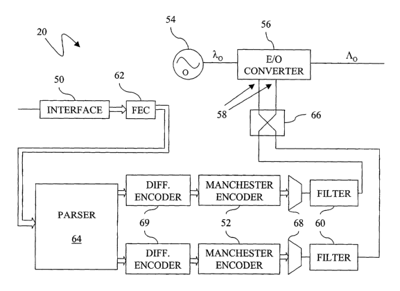
facilitate processing the signal, such as for FEC encoding
17
CA 02458440 2004-02-23
WO 03/019240 PCT/US02/26858
and parsing. For example, in some circumstances it is more
practical to perform parallel processing on two or more lower
bit rate signals than it is to perform the same operation on
a single, high bit rate signal. Some, none, or all of the
data processing in the transmitter 20 can be performed with
several parallel, lower bit rate signals. Multiplexers 68,
sometimes referred to as "serializers", are also included in
that embodiment to combine parallel data signals into a
higher bit rate serial data signals.
[0063] Fig. 12 shows a signal profile of the optical data
signal no when the parsed and coupled data signals of Fig. 11
are input to the E/O converter 56. In that embodiment, one of
the data signals is upconverted to a data signal at a longer
wavelength than the optical carrier ~,o, the other sideband is
upconverted to a sideband at a shorter wavelength than the
optical carrier ~,o, and the optical carrier ~,o is suppressed.
[0064] Fig. 13 shows another signal profile of the optical
data signal no. That signal profile can be produced by an
embodiment of the transmitter 20 in which the parser 64
separates the data signal into signals having different bit
rates and, therefore, different frequencies. As a result, the
different data signals will be offset differently from the
optical carrier ~,o. Typically, the lower bit rate signal will
also have more narrow frequency and wavelength spectrums. In
other embodiments, the optical data signals can be on
opposite sides of the optical carrier ~,o, and in other
embodiments there can be more than two parsed data signals
having more than two different bit rates.
[0065] Fig. 14 shows another embodiment of the transmitter
20 including differential encoders 69. The parser 64,
differential encoders 69, and Manchester encoders 52 can be
implemented, for example, as one or more field programmable
gate arrays, application specific integrated circuits,
general purpose integrated circuits, or other integrated
circuits. Furthermore, the differential encoders 69, as well
as other devices, may be implemented in other embodiments of
18
CA 02458440 2004-02-23
WO 03/019240 PCT/US02/26858
the invention, such as embodiments without the parser 64.
Furthermore, the differential encoder may be replaced with
other encoders, such as duobinary encoders.
[0066] Fig. 15 shows another embodiment of the transmitter
20 in which the parser 64 is used and the coupler 66 is
eliminated. In that embodiment, an optical carrier source 54
and an E/0 converter 56 are provided for each parsed signal.
For example, both parsed data signals can be provided at the
same bit rate, but optical carriers ~,o having different
wavelengths can be used so that the data signals are
upconverted onto different frequencies. In other embodiments,
the optical carrier sources 54 can produce optical carriers
~,o having the same wavelength and, for example, one parsed
data signal can be upconverted onto a sideband having a
longer wavelength than the optical carrier ~,o, and the other
parsed data signal can be upconverted onto a sideband having
a shorter wavelength than the optical carrier ~,o. In other
embodiments, the parser 64 can separate the data signal into
more than two signals, and more than two optical carrier
sources 54 and an E/O converters 56 can also be used.
[0067] Fig. 16 shows a circuit schematic of one embodiment
of the parser 64, differential encoders 69, and Manchester
encoders 52. That embodiment can be, for example, in the form
of an integrated circuit, such as an application specific
integrated circuit, a field programmable gate array, a
general purpose integrated circuit, other integrated
circuits, or discrete components.
[0068] Fig. 17 shows another embodiment of a portion of
the transmitter 20 around the filter 60. That embodiment
includes a first amplifier 70 in front of the filter 60, a
second amplifier 70 after the filter 60, and a feedback loop
including a processor 72. The first amplifier 70 and the
feedback loop provide controlled signal gain to compensate
for variations in the data signal. For example, one or more
parameters (e. g., gain and gain profile) of the first
amplifier 70 can be controlled through the feedback loop,
19
CA 02458440 2004-02-23
WO 03/019240 PCT/US02/26858
which can include the processor 72 and/or other circuitry,
such as an application specific integrated circuit, a general
purpose integrated circuit, a field programmable gate array,
and discrete components, to process the feedback signal and
control the first amplifier 70. The second amplifier 70
provides additional gain, and it can be eliminated if
sufficient gain is provided by the first amplifier 70. This
embodiment can be modified, such as to utilize a feedforward
loop, to utilize more or less amplifiers 70, to vary the
location of the amplifiers 70, etc.
[0069] Fig. 24 illustrates one embodiment of the filter
60. In that embodiment, the filter 60 includes a low pass
stage and a high pass stage which collectively act as a band
pass filter. The low pass stage is illustrated as an
amplifier, such as a gain limiting amplifier, and the high
pass stage is illustrated as a passive filter, such as a
passive Bessel filter, although other types of amplifiers,
filters, or other devices may be used, and the filter may
include active or passive stages. In some embodiments, the
order in which the stages are arranged and the number of
stages may be changed. In other embodiments, one or more of
the amplifiers 70 illustrated in Fig. 17 may operate as one
or more of the filter stages, such as the gain limiting
amplifier. In other embodiments, the filter 60 may be a
filter other than a band pass filter. The filter 60 may be
used, for example, to facilitate duobinary encoding by
selecting filter characteristics which compliment the
differential encoder 69 or other devices.
[0070] Fig. 18 shows an embodiment of the transmitter
interface 50 including a short reach interface ("SRI")
receiver 74 and a SONET performance monitor 76. In the
illustrated embodiment, the SRI 74 converts the incoming data
signal into two or more parallel, lower bit rate signals. For
example, the SRI can convert an optical OC-192 signal into
sixteen parallel, 622 Mbps electrical signals. The SONET
performance monitor 76, for example, can perform section
monitoring and termination functions.
CA 02458440 2004-02-23
WO 03/019240 PCT/US02/26858
[0071] Fig. 19 shows a receiver 22 including a filter 80,
an optical to electrical ("O/E") converter 82, and an
interface 84. That receiver 22 can receive the optical data
signals generated by the transmitters 20 of the present
invention without the need for Manchester, differential, or
duobinary decoders. The receiver 22 can also include other
features, such as FEC decoding, assembling two or more data
signals, automatic gain control ("AGC"), clock and data
recovery ("CDR"), deserializing, etc.
[0072] The filter 80 filters one or more signals from the
incoming optical data signal no. For example, in a WDM system
10 the filter can be used to select among the several signals
and to reduce the noise in the optical data signal no, while
in a single channel system 10 the filter 80 can be used to
filter noise. In some embodiments, such as single channel
systems where noise is not of concern, the filter 80 can be
eliminated. The filter 80 can be a single stage or multiple
stage filter, can be a single pass or a multiple pass filter,
and can utilize one or more types of filters. For example,
the filter 80 can have one stage including one or more fiber
Bragg gratings and another stage including one or more Mach-
Zehnder interferometric filters. The filter 80 can also
include other types of ffilters, such as a fiber Bragg Fabry-
Perot filter, a notched filter, a phase shifted filter, a
bulk grating, etc., and can, for example, provide one or more
filtered signals to one or more receivers 22. Many other
types and combinations of filters 80 are also possible.
[0073) The O/E converter 82 converts the optical data
signal no into one or more corresponding electrical signals.
The interface 84 provides a connection for data being
received and is analogous to the interface 50 in the
transmitter 20.
[0074] Fig. 20 shows another embodiment of the receiver 22
including a FEC decoder 86. That receiver 22 can be used to
receive data signals which are FEC encoded, such as can be
transmitted by the transmitter 20 illustrated in Fig. 10.
21
CA 02458440 2004-02-23
WO 03/019240 PCT/US02/26858
[0075] Fig. 21 shows another embodiment of the receiver 22
including an assembler 88 that can be used to receive
separated data signals, such as those transmitted by the
transmitter 20 illustrated in Fig. 11. In that embodiment,
the received optical signal is split between two filters 80,
each of which filters one of the signals to be received. In
other embodiments, the separate filters 80 can be replaced by
a single filter (e. g. a bulk grating or an arrayed waveguide)
which can separate from the incoming signal no the two or
more data signals of interest. The filtered signals are
converted to electrical form by the O/E converters 82, and
the electrical signals are combined by the assembler 88. In
other embodiments, more than two signals can be assembled.
The illustrated embodiment also includes a FEC decoder 86
which decodes the forward error correction encoded signals.
[0076] Fig. 22 shows another embodiment of the receiver 22
that includes automatic gain controllers ("AGC") 90, clock
and data recovery ("CDR") circuits 92, and demultiplexers 94,
which are sometimes referred to as "deserializers". The
demultiplexers 94 separate a serial data signal into plural
lower bit rate data signals, which are assembled by the
assembler 88. The assembler 88 produces the assembled data as
several separate data signals which are FEC decoded and
combined into a single signal by the interface 84. The
demultiplexing or deserializing of the data signal. into
several lower bit rate signals facilitates further processing
of the signal, such as assembling and FEC decoding. For
example, in some circumstances it is more practical to
perform parallel processing on several lower bit rate signals
than it is to perform the same operation on a single, high
bit rate signal. Some or all of the data processing in the
receiver 22 can be done with several parallel low bit rate
signals.
[0077] Fig. 23 shows an embodiment of the receiver
interface 74 including a SONET performance monitor 96 and a
short reach interface ("SRI") transmitter 98. The SONET
performance monitor 96, for example, can perform section
22
CA 02458440 2004-02-23
WO 03/019240 PCT/US02/26858
monitoring and termination functions. The SRI 98 combines the
parallel data signal into a higher bit rate, serial signal.
The receiver interface 74 is analogous to the transmitter
interface 50.
[0078] Fig. 25 illustrates one embodiment of a filter 80
which may be used, for example, in the receiver 22. In that
embodiment, the filter 80 includes one periodic filter stage,
such as a Mach-Zehnder filter, and one band filter, such as a
Bragg grating filter. Other types of periodic and band
filters may be used in the filter 80. In other embodiments,
the order of the stages may be different, the filter 80 may
include more or less stages, different types of stages, and
different types of filters.
[0079] Many variations and modifications can be made to
the present invention without departing from its scope. For
example, advantages of the present invention can be realized
with different numbers, configurations, and combinations of
components in the transmitters 20 and receivers 22.
Similarly, different numbers and forms of electrical and
optical data signals can also be utilized with the present
invention. Many other variations, modifications, and
combinations are taught and suggested by the present
invention, and it is intended that the foregoing
specification and the following claims cover such variations,
modifications, and combinations.
23