Language selection

Search

Patent 2458638 Summary

Third-party information liability

Some of the information on this Web page has been provided by external sources. The Government of Canada is not responsible for the accuracy, reliability or currency of the information supplied by external sources. Users wishing to rely upon this information should consult directly with the source of the information. Content provided by external sources is not subject to official languages, privacy and accessibility requirements.

Claims and Abstract availability

Any discrepancies in the text and image of the Claims and Abstract are due to differing posting times. Text of the Claims and Abstract are posted:

  • At the time the application is open to public inspection;
  • At the time of issue of the patent (grant).
(12) Patent Application: (11) CA 2458638
(54) English Title: OPTICAL STORAGE MEDIUM AND METHOD OF MANUFACTURING SAME
(54) French Title: SUPPORT DE DONNEES OPTIQUE ET PROCEDE DE FABRICATION ASSOCIE
Status: Dead
Bibliographic Data
(51) International Patent Classification (IPC):
  • G11B 7/00 (2006.01)
  • G11B 7/24 (2006.01)
  • G11B 7/26 (2006.01)
(72) Inventors :
  • VROMANS, PETRUS H. G. M. (Netherlands (Kingdom of the))
  • UBBENS, IGOLT P. D. (Netherlands (Kingdom of the))
  • DECRE, MICHEL M. J. (Netherlands (Kingdom of the))
(73) Owners :
  • KONINKLIJKE PHILIPS ELECTRONICS N.V. (Netherlands (Kingdom of the))
(71) Applicants :
  • KONINKLIJKE PHILIPS ELECTRONICS N.V. (Netherlands (Kingdom of the))
(74) Agent: SMART & BIGGAR
(74) Associate agent:
(45) Issued:
(86) PCT Filing Date: 2002-08-26
(87) Open to Public Inspection: 2003-03-06
Availability of licence: N/A
(25) Language of filing: English

Patent Cooperation Treaty (PCT): Yes
(86) PCT Filing Number: PCT/IB2002/003527
(87) International Publication Number: WO2003/019541
(85) National Entry: 2004-02-25

(30) Application Priority Data:
Application No. Country/Territory Date
01203258.7 European Patent Office (EPO) 2001-08-29

Abstracts

English Abstract


The invention describes an optical data storage medium comprising a substrate
(2), a spacer layer (5) and a cover layer (8). The medium comprises two
information layers (3, 4) and (6, 7). The invention further describes methods
of manufacturing such an information medium (1), which relate to the manner in
which the information layers are provided with data patterns. The invention
further discloses a method wherein an UV light (10)-transparent stamper (9) is
used in combination with a photopolymerization lacquer and/or pressure-
sensitive adhesives.


French Abstract

L'invention concerne un support de données optique comprenant un substrat (2), une couche d'espacement (5) et une couche de recouvrement (8), ainsi que deux couches de données (3, 4) et (6, 7). La présente invention porte également sur des procédés pour fabriquer un support d'information (1) de ce type, lesquels concernent la manière dont les couches de données sont dotées de schémas de données. Enfin, cette invention porte aussi sur un procédé, selon lequel une matrice (9) transparente à la lumière ultraviolette (10) est utilisée en combinaison avec un vernis photopolymérisable et/ou des adhésifs autocollants.

Claims

Note: Claims are shown in the official language in which they were submitted.


7

CLAIMS:

1. An optical storage medium (1) which successively comprises
i) a substrate (2),
ii) a first data pattern (3) of pits/grooves
iii) a first stack (4) of layers adjoining the first data pattern (3)
iv) a spacer (5)
v) a second stack (6) of layers
vi) a second data pattern (7) of pits/grooves, and
vii) a cover (8), characterized in that the storage medium (1) can be
considered
to be composed of elements that are interconnected, said elements successively
being:
a) a substrate (2) provided with the first data pattern (3) of pits/grooves
over
which the first stack (4) of layers is provided,
b) a spacer (5),
c) a cover (8) provided with the second data pattern (7) of pits/grooves over
which the second stack (6) of layers is provided, said second stack (6) of
layers lying against
the spacer (b), (5).

2. An optical storage medium (1) that successively comprises
i) a substrate (2),
ii) a first data pattern (3) of pits/grooves,
iii) a first stack (4) of layers adjoining the first data pattern (3)
iv) a spacer (5)
v) a second stack (6) of layers,
vi) a second data pattern (7) of pits/grooves,
vii) a cover (8), characterized in that the storage medium can be considered
to
be composed of elements that are interconnected, which elements successively
are:
a) a substrate (2) provided with the first data pattern (3) of pits/grooves
over
which the first stack (4) of layers is provided


8

d) a spacer (5) provided with the second stack (6) of layers over which the
second data pattern (7) of pits/grooves is provided, said second data pattern
(7) being
separated from the first data pattern (3) by the spacer (5),
e) a cover (8).

3. An optical storage medium (1) that successively comprises
i) a substrate (2),
ii) a first data pattern (3) of pits/grooves
iii) a first stack (4) of layers adjoining the first data pattern (3)
iv) a spacer (5)
v) a second stack (6) of layers,
vi) a second data pattern (7) of pits/grooves, and
vii) a cover (5), characterized in that the storage medium (1) can be
considered
to be composed of elements that are interconnected, which elements
successively are:
f) a substrate (2),
g) a spacer (5) provided with the first stack (4) of layers over which the
first
data pattern (3) of pits/grooves is provided, said first data pattern lying
against the substrate
(2),
c) a cover (5) provided with the second data pattern (7) of pits/grooves over
which the second stack (6) of layers is provided, said second stack (6) of
layers lying against
the spacer (g), 5).

4. An optical storage medium (1), which successively comprises
i) a substrate (2),
ii) a first data pattern (3) of pits/grooves,
iii) a first stack (4) of layers adjoining the first data pattern (3),
iv) a spacer (5)
v) a second stack (6) of layers,
vi) a second data pattern (7) of pits/grooves, and
vii) a cover (5), characterized in that the storage medium (1) can be
considered
to be composed of elements that are interconnected, which elements
successively are:
f) a substrate (2),
h) a spacer (5) which is provided, on one side, with the first data pattern
(3) of
pits/grooves over which the first stack (4) of layers is provided, and, on the
other side, with


9


the second data pattern (7) of pits/grooves over which the second stack (6) of
layers is
provided, and
e) a cover (8).
5. A method of manufacturing an optical storage medium (1) as claimed in
claims 1, 3, characterized in that the element c) is obtained by means of the
following steps:
c1) providing the cover material with an auxiliary substrate,
c2) applying a photopolymerizable lacquer to the cover material,
c30 placing a stamper on the photopolymerizable lacquer,
c40 carrying out a polymerization reaction and removing the stamper,
c5) sputtering a stack of layers onto the structured photopolymerizable
lacquer, and
c6) removing the auxiliary substrate.
6. A method of manufacturing an optical storage medium (1) as claimed in claim
2, characterized in that element d) is obtained by means of the following
steps:
d1) applying a photopolymerizable lacquer to a stamper,
d2) carrying out a polymerization treatment, and
d3) connecting the lacquer polymerized in step d2) to a spacer (5),
d4) removing the stamper,
d5) sputtering a stack of layers onto the structured photopolymerizable
lacquer.
7. A method of manufacturing an optical storage medium (1) as claimed in
claims 2-3, characterized in that element d) or g) is obtained by means of the
following steps:
d6) applying a stack (6) of layers to a stamper,
d7) applying a photopolymerizable lacquer to the stack (6) of layers, and
d8) carrying out a polymerization reaction so as to form a structured
photopolymerizable lacquer that is provided with a stack of layers (6).
8. A method of manufacturing an optical storage medium (1) as claimed in claim
2, characterized in that element d) is obtained by means of the following
steps:
d9) providing the spacer (5) on the element a),


10


d10) placing an UV radiation (10)-transparent stamper (9) on the spacer (5) of
step d9),
d11) carrying out a polymerization reaction,
d12) removing the transparent stamper (9), and finally
d13) sputtering a stack (6) of layers onto the structured photopolymerizable
lacquer as obtained after step d11).
9. A method of manufacturing an optical storage medium (1) as claimed in claim
8, characterized in that steps d9)-d10) are divided into four sub-steps, i.e.:
d14) providing the spacer (5) on element a)
d15) carrying out a polymerization reaction,
d16) providing an additional spacer on the polymerized spacer of d15), and
d17) placing the UV radiation (10)-transparent stamper (9) on said additional
spacer of d16).
10. A method of manufacturing an optical storage medium (1) as claimed in
claims 1-4, characterized in that one or more of the elements a)-g) are
interconnected by
means of a pressure-sensitive adhesive or a photopolymerization lacquer.

Description

Note: Descriptions are shown in the official language in which they were submitted.


CA 02458638 2004-02-25
WO 03/019541 PCT/IB02/03527
Optical storage medium and method of manufacturing same
The invention relates to an optical storage medium which successively
comprises
i) a substrate,
ii) a first data pattern of pits/grooves
iii) a first stack of layers adjoining the first data pattern
iv) a spacer
v) a second stack of layers
vi) a second data pattern of pits/grooves, and
vii) a cover.
Such an optical storage medium is known from, for example, United States
patent specification 5,679,429. A polycarbonate substrate obtained by
injection molding and
comprising a data pattern was provided with a reflection layer of amorphous
silicon carbide
by means of sputtering. The disc thus composed was placed in a spin coater,
after which a
spacer layer of an UV-curable photopolymer was provided while rotating said
disc. After
curing of this spacer layer, a second photopolymer layer was provided thereon
and cured.
Subsequently, a third photopolymer layer was provided, after which a stamper,
which
comprises a negative of the second data pattern, was brought into contact with
the non-cured,
third photopolymer that was subsequently cured by exposure to UV radiation,
after which the
stamper was carefully removed. A reflection layer was applied to the second
data pattern thus
provided, which reflection layer was finally provided with a cover.
One of the trends in optical storage media is to increase the storage
capacity.
This object can be achieved by reducing the laser wavelength ~, and/or by
increasing the
numerical aperture (NA) as the dimension of the laser spot is proportional to
(~,/NA)2.
Alternatively, this can be achieved by using multiple recording layers.


CA 02458638 2004-02-25
WO 03/019541 PCT/IB02/03527
2
An object of the invention is, inter alia, to provide an optical storage
medium
that can be considered to be composed of elements that are interconnected,
which elements
are individually manufactured.
In accordance with the invention, this object is achieved in that the above-
mentioned elements of the storage medium successively are:
a) a substrate provided with the first data pattern of pits/grooves over which
the first stack of layers is provided,
b) a spacer,
c) a cover provided with the second data pattern of pits/grooves over which
the
second stack of layers is provided, said second stack of layers lying against
the spacer b).
In a particular embodiment of the invention, the storage medium can be
considered to be composed of elements that are interconnected, said elements
successively
being:
a) a substrate provided with the first data pattern of pits/grooves, over
which
1 S the first stack of layers is provided,
d) a spacer provided with the second stack of layers over which the second
data pattern of pits/grooves is provided, said second data pattern being
separated from the
first data pattern by the spacer,
e) a cover.
In accordance with a different, preferred embodiment, the storage medium in
question can be considered to be composed of elements that are interconnected,
said elements
successively being:
f) a substrate,
g) a spacer provided with the first stack of layers over which the first data
pattern of the pits/grooves is provided, said first data pattern lying against
the substrate,
c) a cover provided with the second data pattern of pits/grooves over which
the
second stack of layers is provided, said second stack lying against the spacer
g).
In accordance with yet another embodiment of the invention, the optical
storage medium can be considered to be composed of elements that are
interconnected, said
elements successively being:
f) a substrate,
h) a spacer that is provided, on one side, with the first stack of layers over
which the first data pattern of pits/grooves is provided, and, on the other
side, with the second
stack of layers over which the second data pattern of pits/grooves is
provided, and


CA 02458638 2004-02-25
WO 03/019541 PCT/IB02/03527
3
e) a cover.
The transparent substrate employed in the optical storage medium in question
can be composed of any polymeric material enabling pitslgrooves to be formed
therein with a
view to forming a data pattern, such as polycarbonate or an amorphous
polyolefin compound.
Alternatively, use can be made of a flat substrate of, for example, glass or
polymethylinethacrylate, in which case the data pattern of pits and/or grooves
is formed by
means of photopolymer replication.
The spacer used in the optical storage medium in question may be a polymer,
such as a radiation-curable polymer. The transparent spacer layer must be
thick enough to
enable a laser source to focus on the first data pattern as well as on the
second data pattern,
whereby interference must be reduced to a minimum. The reflection layer used
in the optical
storage medium in question is, in particular, a metal layer having a high
reflection at the laser
wavelength used to reproduce the data patterns. Examples of suitable metals
are aluminum,
gold, silver, copper and alloys thereof.
The invention further relates to a method of manufacturing an optical storage
medium, which method is characterized in that the element c) in question is
obtained by
means of the following steps:
c1) providing the cover material with an auxiliary substrate,
c2) applying a photopolymerizable lacquer to the cover material,
c3) placing a stamper on the photopolymerizable lacquer,
c4) carrying out a polymerization reaction and removing the stamper,
c5) sputtering a stack of layers onto the structured photopolymerizable
lacquer, and
c6) removing the auxiliary substrate.
In a particular embodiment it is particularly preferred that the above-
mentioned element d) is obtained by means of the following steps:
d1) applying a photopolymerizable lacquer to a stamper,
d2) carrying out a polymerization treatment, and
d3) connecting the lacquer polymerized in step d2) to a spacer,
d4) removing the stamper,
d5) sputtering a stack of layers onto the structured photopolymerizable
lacquer.
In another embodiment, the method in question is characterized in that the
above-mentioned element d) or g) is obtained by means of the following steps:


CA 02458638 2004-02-25
WO 03/019541 PCT/IB02/03527
4
d6) applying a stack of layers to a stamper,
d7) applying a photopolymerizable lacquer to the stack of layers, and
d8) carrying out a polymerization reaction so as to form a structured
photopolymerizable lacquer that is provided with a stack of layers.
In yet another embodiment, the method in question is characterized in that the
above-mentioned element d) is obtained by means of the following steps:
d9) providing the spacer on the element a),
d10) placing an UV radiation-transparent stamper on the spacer of step d9),
dl l) carrying out a polymerization reaction,
d12) removing the stamper, and finally
d13) sputtering a stack of layers onto the structured photopolymerizable
lacquer as obtained after step d11).
In a refinement of the last-mentioned embodiment, steps d9)-d10) are divided
into four sub-steps, i.e.:
d14) providing the spacer on the element a)
d15) carrying out a polymerization reaction,
d16) providing an additional spacer on the polymerized spacer of d15), and
d17) placing an W radiation-transparent stamper on said additional spacer of
d16).
The transparent stamper may be, for example, a transparent synthetic resin
substrate that can be manufactured using a known nickel stamper in an
injection molding
process. The transparent substrate may comprise the same materials as those
mentioned
above in the description of the optical storage medium.
In addition, one or more of the above elements a)-g) may be interconnected by
means of a pressure-sensitive adhesive (PSA) or a photopolymerization lacquer
(2p).
These and other aspects of the invention are apparent from and will be
elucidated with reference to the embodiments described hereinafter.
In the drawings:
Fig. 1 shows a finished optical storage medium in accordance with the
invention,


CA 02458638 2004-02-25
WO 03/019541 PCT/IB02/03527
Fig. 2 shows a particular embodiment of the optical storage medium in
accordance with the invention,
Fig. 3 shows a different embodiment of the optical storage medium in
accordance with the invention,
Fig. 4 shows yet another embodiment of the optical storage medium in
accordance with the invention, and
Fig. 5 shows a further embodiment of the optical storage medium in
accordance with the invention.
In Fig. 1, an optical storage medium 1 comprises, in succession, a substrate
2,
a first data pattern of pits/grooves 3, a first stack 4 of layers adjoining
the first data pattern 3,
a spacer 5, a second stack 6 of layers, a second data pattern of pits/grooves
7 and, finally, a
cover 8.
1 S A particular embodiment of the optical storage medium 1 in accordance with
the invention is diagrammatically shown in Fig. 2, which Figure can be
considered to be a
combination of three separate parts, i.e. a substrate 2 provided with the
first data pattern of
pits/grooves 3 over which the first stack 4 of layers is provided, a spacer 5
and, finally, a
cover 8 that is provided with the second data pattern of pits/grooves 7 over
which the second
stack 6 of layers is provided.
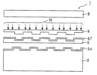
Fig. 3 shows a particular embodiment of the optical storage medium 1 in
accordance with the invention, which optical storage medium 1 can be
considered to be
composed of three individual parts, i.e. a substrate 2 provided with the first
data pattern of
pits/grooves 3 over which the first stack 4 of layers is provided, a spacer 5
that is provided
with the second stack 6 of layers and the second data pattern of pits/grooves
7, and a cover 8.
The data pattern of pits/grooves 7 is provided by means of an UV radiation-
transparent
stamper 9 by carrying out a polymerization reaction caused by W radiation 10
that is
projected through the transparent stamper 9.
Fig. 4 shows a particular embodiment of the optical storage medium 1 in
accordance with the invention, which optical storage medium 1 is to be
considered to be a
combination of three individual parts, i.e. a substrate 2, a spacer 5 provided
with the first
stack 4 of the layers and the first data pattern of pits/grooves 3, and a
cover 8 that is provided
with the second data pattern of pits/grooves 7 and the second stack 6 of
layers.


CA 02458638 2004-02-25
WO 03/019541 PCT/IB02/03527
6
Fig. S diagrammatically shows yet another embodiment of the optical storage
medium 1 in accordance with the invention, which optical storage medium 1 can
be
considered to be a combination of individual pasts, i.e. a substrate 2, a
spacer 5 that is
provided, on one side, with the first data pattern 3 of pits/grooves over
which the first stack 4
of layers is provided, and, on the other side, with the second data pattern 7
of pitslgrooves
over which the second stack 6 of layers is provided.

Representative Drawing
A single figure which represents the drawing illustrating the invention.
Administrative Status

For a clearer understanding of the status of the application/patent presented on this page, the site Disclaimer , as well as the definitions for Patent , Administrative Status , Maintenance Fee  and Payment History  should be consulted.

Administrative Status

Title Date
Forecasted Issue Date Unavailable
(86) PCT Filing Date 2002-08-26
(87) PCT Publication Date 2003-03-06
(85) National Entry 2004-02-25
Dead Application 2007-08-27

Abandonment History

Abandonment Date Reason Reinstatement Date
2006-08-28 FAILURE TO PAY APPLICATION MAINTENANCE FEE

Payment History

Fee Type Anniversary Year Due Date Amount Paid Paid Date
Registration of a document - section 124 $100.00 2004-02-25
Application Fee $400.00 2004-02-25
Maintenance Fee - Application - New Act 2 2004-08-26 $100.00 2004-07-13
Maintenance Fee - Application - New Act 3 2005-08-26 $100.00 2005-07-29
Owners on Record

Note: Records showing the ownership history in alphabetical order.

Current Owners on Record
KONINKLIJKE PHILIPS ELECTRONICS N.V.
Past Owners on Record
DECRE, MICHEL M. J.
UBBENS, IGOLT P. D.
VROMANS, PETRUS H. G. M.
Past Owners that do not appear in the "Owners on Record" listing will appear in other documentation within the application.
Documents

To view selected files, please enter reCAPTCHA code :


To view images, click a link in the Document Description column. To download the documents, select one or more checkboxes in the first column and then click the "Download Selected in PDF format (Zip Archive)" or the "Download Selected as Single PDF" button.

List of published and non-published patent-specific documents on the CPD .

If you have any difficulty accessing content, you can call the Client Service Centre at 1-866-997-1936 or send them an e-mail at CIPO Client Service Centre.


Document
Description 
Date
(yyyy-mm-dd) 
Number of pages   Size of Image (KB) 
Abstract 2004-02-25 1 57
Claims 2004-02-25 4 153
Drawings 2004-02-25 2 23
Representative Drawing 2004-02-25 1 5
Description 2004-02-25 6 279
Cover Page 2004-04-23 1 36
Assignment 2004-02-25 6 202
PCT 2004-02-25 3 108