Note: Descriptions are shown in the official language in which they were submitted.
CA 02458669 2007-07-26
RD24939
SYSTEMS AND METHODS FOR DETECTING IONIZING
RADIATION WITH AN IMAGING SYSTEM
BACKGROUND OF THE INVENTION
This invention relates generally to ionizing radiation imaging systems and,
more
particularly, to systems and methods for coupling a scintillator to a light
imager.
In one common imaging system configuration, an X-ray source projects an X-ray
beam that passes through the object being imaged, such as an aircraft engine
component. The beam, after being attenuated by the object, impinges upon a
detector
having an array of detector elements. The intensity of the radiation beam
received at
the detector is dependent upon the attenuation of the X-ray beam by the
object. Each
detector element of the array produces a separate electrical signal that is
representative of the beam attenuation at the detector location. The
attenuation
measurements from all the detectors are acquired separately to produce an
image.
Multiple images may be taken of the same object, for example, by a series of
rotations, and the set of images processed to form a cross-sectional image of
the X-ray
attenuation of the object.
The radiation imaging system commonly comprises a light imager (e.g., a
photosensor
array) coupled to a scintillator. The photosensor array comprises a plurality
of pixels,
each having a photosensitive element, such as a photodiode, 'and pixels are
configured
into a matrix of rows and several columns, e.g., about one thousand rows and
columns. The scintillator includes scintillation material positioned over the
imager
I
CA 02458669 2004-02-19
WO 03/022017 PCT/US02/26651
array. As described below, the scintillator may be integral with the imager
array, for
use in detecting low energy (radiation less than about 100 keV), or a separate
plate
located over the imager array when the device is used for detection of high
energy
radiation (radiation above about 100 keV). Contact pads are coupled to or
formed on
the imager array adjacent the periphery of the imager array and are associated
with the
respective rows and columns in the imager array. Particularly, the contact
pads
facilitate accessing information from each row and column of the photosensing
element array by enabling electrical contact to external circuitry.
The above-described system sometimes is referred to as a computed tomography
(CT)
system. Although the present invention is sometimes described in the context
of CT
systems, the present invention is not limited to use in connection with CT
systems and
can be utilized with other radiation based imaging systems, such as
radiographic X-
ray systems.
During scanning, X-rays are emitted from the X-ray source in the direction of
the
detector, and each X-ray, which interacts with the scintillator, is converted
into visible
photons in accordance with the scintillator gain. For example, a scintillator
having a
gain of 1000 converts each X-ray from the X-ray source, on average, into 1000
photons. These photons are detected by photosensors that develop an electrical
signal
(e.g., charge accumulation on a photodiode) corresponding to the detected
photons.
This accumulated electrical signal on photosensors in the array is accessed
via the
contact pads and used by readout electronics to provide an estimate of the
location of
the ray event. Further digital processing is used to integrate the signal from
all
elements of the photosensor array, and from multiple images if more than one
scan is
taken, and to form the acquired image.
For low energy radiation, a scintillator deposited directly on the light
imager may be
used. Due to the practical thickness limitations of deposition, on the order
of 1 mm,
for high energy radiation (i.e., radiation above about 100 keV), the
scintillator
typically is a separate plate coupled to the imaging plate so that a surface
of the
scintillating plate is adjacent the imaging plate.
2
CA 02458669 2004-02-19
WO 03/022017 PCT/US02/26651
In small ionizing radiation imagers, utilizing a separate scintillator plate
generally
provides satisfactory results. However, use of a separate scintillator plate
may result
in degradation of image quality in the larger two-dimensional, or area,
ionizing
radiation imagers. For example, directly coupling a large, e.g., greater than
100-cm2
scintillator to a large, e.g., greater than 100-cm2 scintillator, a light
imager suffers
from response variation due to a varying air gap between the scintillator and
the light
imager. In addition, imaging systems utilizing a scintillator coupled to a
light imager
may be susceptible to oversaturation. For example, if an X-ray source emits
approximately 300,000 rays to generate an image, the scintillator produces
approximately 300,000,000 photons. This photon level may exceed the capacity
of
the light imager system circuitry depending on the read time and charge
capacity of
the photosensing element (which in turn depends on the common voltage bias and
area of each element). A typical common bias is about 10 volts (V) and a
typical
element size is about 0.01 to 1.0 mm2. One way to avoid oversaturation is to
perform
multiple readouts. Performing multiple readouts, however, may result in
excessively
long total readout time for the part being imaged and increases noise for a
single
image. Until now, to prevent oversaturation, either the X-ray flux or the
number of
photons generated in the scintillator for each incident ray is reduced.
Reducing the
flux, however, degrades the system signal-to-noise ratio, which is
undesirable.
It would be desirable to provide improved optical quality in high energy
imaging
systems with large imagers. The optical quality can be assessed using two
quantitative measurements. The first quantitative measurement is the
modulation
transfer function (MTF), which represents a measure of the light spread. The
second
quantitative measurement is the detector quantum efficiency, which includes
both the
MTF and the noise terms; therefore, the detector quantum efficiency is a
reflection of
signal-to-noise ratio of the image detectability. It also would be desirable
to reduce
the likelihood of system oversaturation without significantly reducing signal-
to-noise
ratio or increasing readout time. It further would be desirable to provide a
simple
method for fabricating such an improved detector.
BRIEF SUMMARY OF THE INVENTION
3
CA 02458669 2004-02-19
WO 03/022017 PCT/US02/26651
A radiation imaging system is provided comprising a scintillator, an imager
array, and
a lamination layer. The lamination layer bonds and optically couples the
scintillator
to the imager array. The lamination layer is comprised of a lamination
material that is
substantially free from void spaces.
A method for fabricating a radiation imaging system is provided comprising the
steps
of disposing a lamination layer between a light imager and a scintillator to
form a
subassembly. The light imager comprises an imager array, an imaging plate
surface
and a plurality of contact pads. Additional steps include subjecting the
subassembly
to a vacuum; heating the subassembly to a bonding temperature, exerting a
bonding
force on the subassembly, maintaining the vacuum, the bonding temperature and
the
bonding force until the light imager is bonded to the scintillator and the
lamination
layer is comprised of a lamination material that is substantially free from
void spaces.
BRIEF DESCRIPTION OF THE DRAWINGS
Fig. 1 is a side view of a radiation imaging system in accordance with one
embodiment of the present invention.
Fig. 2 is a side view of the bonding fixture supporting the subassembly.
Fig. 3 provides a table illustrating alternative materials for the lamination
layer.
Figures 4, 5, 6 and 7 illustrate a sequence of steps for fabricating the
radiation
imaging system shown in Fig. 1 in accordance with one embodiment of the
present
invention.
Figures 8, 9 and 10 illustrate a sequence of steps for fabricating the
radiation imaging
system shown in Fig. 1 in accordance with another embodiment of the present
invention.
Fig. 11 provides a side view of a radiation imaging system where the
lamination layer
comprises a first lamination layer portion and a second lamination layer
portion, in
accordance with still another embodiment of the present invention.
4
CA 02458669 2004-02-19
WO 03/022017 PCT/US02/26651
DETAILED DESCRIPTION OF THE INVENTION
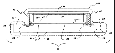
A radiation imaging system 20 of Fig. I comprises a scintillator 26 of Fig. 1,
an
imager array 30 of Fig. 1, and a lamination layer 22 of Fig. 1. The lamination
layer
22 bonds and optically couples scintillator 26 to imager array 30. The
lamination
layer 22 comprises a lamination material that is substantially free from void
spaces.
A light imager 24 of Fig. 1 includes an imager substrate 28, an imaging plate
surface
34 of Fig. 1, imager array 30 and a plurality of contact pads 32 of Fig. 1
(also referred
to as fingers, by way of example and not limitation, only two contact pads 32
are
shown in Fig. 1). Contact pads 32 are formed on a periphery 38 of imaging
plate
surface 34 (the electrical connection of contact pads 32 to the rows and
columns of
the photosensors of imager array 30 is not shown). Imager array 30 is formed
on a
central portion 36 of Fig. 1 of imaging plate surface 34 and includes a matrix
of
photosensor elements, e.g., amorphous silicon-based photodiodes, arranged in
rows
and columns. An intermediate imaging plate surface 35 is comprised of imaging
plate
surface 34 between contact pads 32 and imager array 30.
In an alternate embodiment of the present invention, imager array 30 further
comprises a passivation layer. Lamination layer 22 is disposed in intimate
contact
with passivation layer (not shown in Fig. 1). The passivation layer is
typically, by
way of example and not limitation, either silicon nitride or silicon oxide.
In an alternate embodiment of the present invention, light imager 24 is formed
on a
silicon substrate. Particular examples of the silicon substrate light imager
include a
complementary metal oxide semiconductor (CMOS) camera or a charge coupled
device (CCD) camera.
In one embodiment of the present invention, scintillator 26 comprises a plate
(having,
by way of example and not limitation, a thickness in the range of between
about 500
microns and about 25000 microns) which includes a scintillator first surface
40 of Fig.
1 and a scintillator second surface 42 of Fig. 1. In another embodiment,
scintillator 26
comprises a fiber optic type scintillator (FOS) formed from fiber optic glass
CA 02458669 2004-02-19
WO 03/022017 PCT/US02/26651
scintillator columns disposed perpendicular to scintillator first surface 40.
The FOS
typically further comprises internal absorbers disposed around the fiber optic
columns
so as to reduce lateral scattering of light within scintillator 26.
Alternatively, a
continuous sheet of scintillating material of gadolinium oxysulfate comprises
scintillator 26. Scintillators comprising a continuous sheet of scintillating
material of
gadolinium oxysulfate are commercially available from, for example, Collimated
Holes, Inc., Campbell, Connecticut.
Scintillator second surface 42 typically is substantially optically reflective
(to reflect
photons generated in the scintillator 26 back towards the imager array 30).
Scintillator 26 is considered substantially optically reflective when the
reflectivity of
scintillator second surface 42 is greater than about 90%.
In another embodiment of the present invention, scintillator 26 has a
substantially
columnar structure.
Lamination layer 22 bonds and optically couples imager array 30 and
scintillator first
surface 40. Lamination layer 22 typically has a thickness in a range between
about 5
microns and about 25 microns. Thinner lamination layers typically have less
optical
crosstalk. However, it is more difficult to form a thinner lamination layer
that is
substantially free of void spaces. As used herein, lamination layer
compositions refer
to the volume between the scintillator first surface 40 and the upper surface
of imager
array 30 that is filled with the lamination material.
In one embodiment of the present invention lamination layer 22 is considered
substantially free from void spaces when lamination layer 22 is comprised of
at least
about 90% of lamination material (i.e. no more thatn about 10% voids in
lamination
layer 22).
In another embodiment of the present invention lamination layer 22 is
considered
substantially free from void spaces when lamination layer 22 is comprised of
at least
about 95% of lamination material (i.e. no more thatn about 5% voids in
lamination
layer 22).
6
CA 02458669 2004-02-19
WO 03/022017 PCT/US02/26651
In another embodiment of the present invention lamination layer 22 is
considered
substantially free from void spaces when lamination layer 22 is comprised of
at least
about 99% of lamination material (i.e. no more thatn about 1% voids in
lamination
layer 22).
In accordance with one embodiment of the present invention, lamination layer
22 is
disposed on imager array 30 and scintillator 26 is disposed on lamination
layer 22 so
that scintillator 26 is aligned over imager array 30.
Lamination material in lamination layer 22 comprises an adhesive such that
lamination layer 22 bonds to both imager array 30 and scintillator first
surface 40
when heated to a specified bonding temperature. A subassembly 150, as depicted
in
Figures 5, 6 and 9, is comprised of scintillator 26, lamination layer 22 and
light
imager 24. Fig. 2 provides a side view of a bonding fixture 500 supporting
subassembly 150.
A cover plate 44 of Fig. 1 is disposed in proximity (about 25 microns to about
50
microns) to scintillator second surface 42, or alternatively in contact with
scintillator
second surface 42. Cover plate 44 is coupled to intermediate imaging plate
surface 35
--with---an adhesive ring 46 of Fig-.T,-typically made of epoxy, to -form-a
hermetic seal
80 of Fig. 1. Hermetic seal 80 is disposed to provide ambient moisture
protection for
scintillator, lamination layer and imager array. Cover plate 44 comprises, for
example, a carbon base composite or aluminum. Adhesive ring 46 commonly
comprises a thermoset epoxy that cures at a temperature less than about 100
degrees
C. Typically, epoxy used in adhesive ring 46 is opaque.
Excessive void spaces in lamination layer 22 that remain after bonding will
adversely
affect radiation imaging system performance. The bonding temperature,
pressure, and
duration requirements are specified in column 4 of the table provided as Fig.
3 to
reduce the formation of void spaces during assembly of scintillator 26,
lamination
layer 22 and imager array 30, so as to provide desired lamination layer
characteristics
as outlined herein.
7
CA 02458669 2004-02-19
WO 03/022017 PCT/US02/26651
For amorphous silicon based light imagers, typical bonding temperatures are
limited
to about 250 degrees C to avoid degrading the performance of the amorphous
silicon
photosensitive elements.
Materials suitable for fabricating lamination layer 22 are provided in the
first column
of the table provided in Fig. 3. The table provides lamination materials
selected from
the group consisting of Benzocyclobutene (BCB) thermoset polymers, plasticized
polyetherimide thermoplastic polymers with a glass transition temperature (Tg)
of less
than about 180 degrees C (i.e. a blend of a polyetherimide and a
pentarythrytol
tetrabenzoate), photodefinable BCB thermoset polymers, thermoset polymer
epoxies
with latent heat catalysts, thermoplastic polyester polymers and thermoplastic
acrylic
polymers.
In one embodiment of the present invention, and referring specifically to
column 1 of
the table provided in Fig. 3, lamination layer 22 of Fig. 1 may be fabricated
from a
thermoset polymer Benzocyclobutene (BCB) with mesitylene as a solvent.
Thermoset
polymer Benzocyclobutene (BCB) lamination material is then soft baked to drive
off
the solvent, per the temperature and duration provided in column 3 of the
table
provided as Fig. 3. When utilizing thermoset polymer Benzocyclobutene (BCB)
with
mesitylene as a solvent as the lamination material, the solvent drive off
temperature
and duration is approximately 150 degrees C and approximately 30 minutes,
respectively.
In another embodiment of the present invention, lamination layer 22 may be a
film
fabricated from a plasticized polyetherimide with a Tg of less than about 180
degrees
C. A suitable example of a plasticized polyetherimide with a Tg of less than
about
180 degrees C is a blend of Ultem 1000 with Benzoflex S-552 (Ultem /
Benzoflex
S-552).
Ultem / Benzoflex S-552 is a plasticized polyetherimide blend containing a
range of
between about 5% to about 40% by weight of pentarythrytol tetrabenzoate (also
known as Benzoflex S-552) with a range of between about 60% and about 95% by
weight polyetherimide (Ultem 1000). The Benzoflex S-552 (sold by Velsicol
8
CA 02458669 2004-02-19
WO 03/022017 PCT/US02/26651
Corporation, Rosemont, Illinois) is a plasticizer for Ultem 1000. Ultem 1000
is
commercially available from General Electric Company, Pittsfield,
Massachusetts.
Blending the Benzoflex S-552 into the Ultem 1000 lowers the Tg of UltemOO
1000
from about 220 degrees C to about 180 degrees C for Ultem Benzoflex S-552.
Additionally, the melt viscosity and bonding temperature is lowered from about
300
degrees C for Ultem 1000 to about 250 degrees C for Ultem Benzoflex S-552.
The Ultem / Benzoflex S-552 blend was used to meet the bonding temperature
limitation of about 250 degrees C to avoid degrading the performance of the
amorphous silicon photosensitive elements.
Moreover, in another embodiment, lamination material is applied as a liquid
solution,
for example by coating. One such liquid solution is UltemOO / Benzoflex S-552
of
about 15% to about 20% by weight in anisole (Fig. 3). After coating, the
solvent is
driven off by soft baking for about 30 minutes at about 150 C as noted in
column 3 of
the table provided in Fig. 3.
Another embodiment of the present invention is to use a lamination material
that can
be photodefined. One such material is a photodefinable BCB thermoplastic
polymer
as depicted in the table provided as Fig. 3. In this case, lamination material
is imaged
to remove it selectively, which eliminates the need for the plasma etching or
excimer
laser ablation steps.
Another embodiment of the present invention utilizes a thermoset polymer epoxy
as
lamination material. Thermoset polymer epoxy may be a blend of siloxane
polyimide
(SPI) and a cycloaliphatic epoxy of about equal parts, and about 1% of an
onium salt
catalyst to form a thermoset adhesive blend. Thermoset polymer epoxy is
applied
onto the light imager 24 of Fig. 1 formed on the silicon substrate and the
thermoset
reaction is catalyzed by the onium salt catalyst at a range of between about
150 C and
about 200 C. This process is particularly useful when assembling amorphous
silicon
based light imagers, since the low bonding temperature reduces mechanical
stress in
radiation imaging system 20 due to thermal coefficient of expansion mismatch
9
CA 02458669 2004-02-19
WO 03/022017 PCT/US02/26651
between scintillator 26 and light imager 24. In addition, soft baking
thermoset
polymer epoxy is not required prior to bonding.
Another embodiment of the present invention is to use a polyester
thermoplastic
polymer as a lamination material as depicted in the table provided as Fig. 3.
Portions
of polyester thermoplastic polymer lamination material that extend beyond
scintillator
26 of Fig. 5 are then removed utilizing an excimer laser or oxygen (02)
plasma.
Another embodiment of the present invention is to use an acrylic thermoplastic
polymer as a lamination material as depicted in the table provided as Fig. 3.
Portions
of acrylic thermoplastic polymer lamination material that extend beyond
scintillator
26 of Fig. 5 are then removed utilizing an excimer laser or 02 plasma.
A second column in the table provided as Fig. 3 depicts the solvents to be
utilized
with respective lamination materials listed in the first column. A third
column in the
table provided as Fig. 3 provides the solvent drive off temperatures and
times. A
fourth column in the table provided as Fig. 3 provides the bonding
temperatures and
times. A fifth column in the table provided as Fig. 3 identifies potential
etching
methods. A sixth column in the table provided as Fig. 3 provides general
comments.
The sixth column of the table provides general comments for the respective
lamination material. For example, BCB is a thermoset polymer material, which
has a
thermal coefficient of expansion (TCE) of approximately 50 parts per million
per
Celsius degree (ppm/C). A lamination material with a low TCE is desirable
because
light imager 24 of Fig. I and scintillator 26 typically have a TCE below 10-
ppm!
degree C. By more closely coupling TCE of scintillator material and TCE of
lamination material, the stress in the final assembled radiation imaging
system 20 is
reduced.
In another embodiment of the present invention, lamination layer 22 further
comprises
an optical absorbing material for reducing scintillator light intensity and
any lateral
spread of scintillator light through lamination layer 22. The addition of this
optical
absorbing material reduces the likelihood of oversaturation of the photosensor
array.
CA 02458669 2004-02-19
WO 03/022017 PCT/US02/26651
In this embodiment, lamination layer 22 typically has a thickness in a range
between
about 5 microns and about 12.5 microns. The optical absorbing material
typically
reduces light passing from scintillator 26 by between about 10% and about 90%.
The
optical absorbing material typically comprises an anthraquinone-based dye such
as
diaminoanthraquinone (DAA) or 1-methylamino-4-dihydroxyanthraquinone (DHA).
The maximum absorption of the optical absorbing material is selected to
reasonably
match a peak sensitivity of the photosensor elements of imager array 30
multiplied by
the output of scintillator 26, e.g., approximately 0.6 microns wavelength for
amorphous silicon photodiodes. For example, if lamination layer 22 is about
12.5
microns thick, about 0.5 weight percent to about 5 weight percent of dye in
lamination
material in lamination layer 22 causes an optical absorption change from about
10%
to about 90%.
In addition, while lamination layer 22 is described above in connection with
optical
absorbing anthraquinone based dye, lamination layer 22 may include other
optical
absorbing materials such as sub-micron carbon powders and azo-based dyes.
Furthermore, in some embodiments, lamination layer 22 does not include an
optical
absorbing material.
A bonding fixture 500 of Fig. 2 is designed to facilitate bonding of
subassembly 150
of Fig. 5. Bonding fixture 500 of Fig. 2 has a heater 220 of Fig. 2 disposed
on a
bottom foundation 225 of Fig. 2, so that a heater first side 221 of Fig. 2
contacts
bottom foundation 225. A vacuum tray 210 of Fig. 2 is disposed on heater 220,
so
that a vacuum tray first side 211 of Fig. 2 is disposed on a heater second
side 222 of
Fig. 2. Vacuum tray 210 is configured with at least one bottom vacuum coupling
230
of Fig. 2. Vacuum tray 210 is configured to have a plurality of vacuum tray
vent slits
208 of Fig. 2 machined into a vacuum tray second side 212 of Fig. 2. Vacuum
tray
210 is configured with internal passages that connect bottom vacuum coupling
230
with vacuum tray vent slits 208. A gasket 205 of Fig. 2 about 50 microns (2
mils)
thick is placed on vacuum tray second side 212. Gasket 205 covers vacuum tray
second surface 212. Gasket 205 has a plurality of gasket vent slits 209 of
Fig. 2 that
are in communication with vacuum tray vent slits 208 that are machined in
vacuum
11
CA 02458669 2004-02-19
WO 03/022017 PCT/US02/26651
tray 210. A fixture cover 200 of Fig. 2 is configured to have two couplings.
The first
coupling is' a vent coupling 260 of Fig. 2 and a second coupling is used
jointly as a
coupling for a top vacuum coupling 250 of Fig. 2 and an inert gas coupling 240
of
Fig. 2. The inert gas typically utilized is either nitrogen or argon.
A polyimide film is utilized as the material for both a bladder 206 of Fig. 2
and gasket
205 to assist in reducing leakage through a periphery seal 290 of Fig. 2 when
pressure
is established in a bottom chamber 400 of Fig. 2 of bonding fixture 500.
Polyimide
film used in gasket 205 also assists in preventing subassembly 150 from
adhering to
vacuum tray second side 212 during bonding. After subassembly 150 of Fig. 5
has
bonded and cooled to a safe handling temperature and subsequently removed from
vacuum tray 210 of Fig. 2, gasket 205 is removed from subassembly 150.
In one embodiment of the present invention, a Kapton polyimide film (a
registered
trademark of E.I. du Pont de Nemours and Company 1007 Market Street,
Wilmington, Delaware 19898) is utilized as material for both bladder 206 and
gasket
205.
In one embodiment of the present invention, radiation imaging system 20 of
Fig. 1 is
fabricated comprising the steps of disposing lamination layer 22 of Fig. 5
between
light imager 24 and scintillator 26 to form subassembly 150. Light imager 24
comprises an imager array 30, an imaging plate surface 34 and contact pads 32.
In the
next step, subassembly 150 is then subjected to a vacuum, which is followed by
heating subassembly 150 to a bonding temperature. Subsequently, a bonding
force is
exerted on subassembly 150. The vacuum, bonding temperature and bonding force
are maintained until light imager 24 is bonded to scintillator 26 and
lamination layer
22 is comprised of lamination material that is substantially void free.
Figures 4, 5, 6 and 7 illustrate a detailed sequence of steps for forming
radiation
imaging system 20 of Fig. 1. In one embodiment of the present invention,
lamination
layer 22 is formed from a liquid solution such as Ultem / Benzoflex 5-552 of
about
15% to 20% by weight in anisole.
12
CA 02458669 2004-02-19
WO 03/022017 PCT/US02/26651
Referring to Fig. 4, lamination layer 22 is disposed on light imager 24
including
imager array 30, intermediate imaging plate surface 35 of imaging plate
surface 34
and contact pads 32. Intermediate imaging plate surface 35 is comprised of
imaging
plate surface 34 between imager array 30 and contact pads 32. Lamination layer
22 is
commonly disposed to light imager 24 by the process of, for example, spinning,
spraying, or meniscus coating. Multiple coats are disposed, if needed, to
achieve the
desired thickness of lamination layer 22.
Light imager 24 and lamination layer 22 are then soft baked as required, to
drive off
excess solvent from lamination layer 22. The soft baking is performed per the
solvent
drive off temperature and time specified in column 3 for the respective
lamination
material of column 1 of the table provided in Fig. 3. This soft baking process
step is
accomplished prior to disposing scintillator 26 onto lamination layer 22.
Referring to Fig. 5, scintillator 26 is disposed on lamination layer 22, so
that
scintillator first surface 40 is disposed on lamination layer 22. Scintillator
26 is also
positioned to cover imager array 30 to produce subassembly 150 as shown in
Fig. 5.
Referring to Fig. 6, in another embodiment of the present invention,
subassembly 150
is produced by removing lamination layer 22 from intermediate imaging plate
surface
35 and contact pads 32. For example, plasma etching in oxygen (or
alternatively,
other appropriate gasses) can accomplish the lamination layer 22 removal from
intermediate imaging plate surface 35 and contact pads 32. Alternatively
lamination
layer 22 is removed from intermediate imaging plate surface 35 and contact
pads 32
by excimer laser ablation using scintillator 26 as the etching mask. Specific
etching
methods for each respective lamination material are depicted in column 5 of
the table
provided as Fig. 3.
In one embodiment of the present invention, the removal of lamination layer 22
of
Fig. 5 from intermediate imaging plate surface 35 and contact pads 32 can be
accomplished prior to bonding subassembly 150.
13
CA 02458669 2004-02-19
WO 03/022017 PCT/US02/26651
In another embodiment of the present invention, the removal of lamination
layer 22
from intermediate imaging plate surface 35 and contact pads 32 can be
accomplished
after bonding subassembly 150.
Gasket vent slits 209 of Fig. 2 of gasket 205 are disposed on vacuum tray 210
so as to
communicate with vacuum tray vent slits 208.
According to one embodiment of the present invention, a first side 90 of
subassembly
150 is disposed on gasket 205 of Fig. 2, so as to cover gasket vent slits 209
and
vacuum tray vent slits 208.
According to another embodiment of the present invention, a first side 90 of
Fig. 2 of
subassembly 150 is disposed on gasket 205, so that subassembly 150 covers
gasket
vent slits 209 and vacuum tray vent slits 208.
A bladder 206 about 50 microns (2 mils) thick is disposed so as to cover
subassembly
150 as shown in Fig. 2. Bladder 206 also covers gasket 205 at a vacuum tray
periphery 213 to form bottom chamber 400 between bladder 206 and vacuum tray
210. Fixture cover 200 is positioned such that a fixture cover first side 201
contacts
bladder 206 at vacuum tray periphery 213 to form a top chamber 100 between
fixture
cover first side 201 and bladder 206.
A top foundation 215 is placed in contact with a fixture cover second side
202.
Fixture cover first side 201, bladder 206, gasket 205 and vacuum tray second
side 212
comprise periphery seal 290.
A bottom chamber absolute pressure of no more than about 13 kPa (100
millimeters
(mm) of mercury (Hg)) is then established and maintained in bottom chamber 400
through bottom vacuum coupling 230. Heater 220 heats subassembly 150 to a
bonding temperature after bottom chamber absolute pressure is established.
Heat
from heater 220 is transferred to subassembly 150 through vacuum tray 210 and
gasket 205.
14
CA 02458669 2004-02-19
WO 03/022017 PCT/US02/26651
When subassembly 150 reaches the bonding temperature per column 4 for the
respective lamination material of column 1 of the table provided in Fig. 3,
inert gas is
admitted through inert gas coupling 240 of Fig. 2 to pressurize and maintain
an
absolute pressure range of between about 170 kPa (10 psig) and about 377 kPa
(40
psig) in top chamber 100. The pressure in top chamber 100 provides the bonding
force. The bottom chamber pressure conditions, top chamber pressure conditions
(bonding force) and bonding temperature conditions are then maintained until
light
imager 24 of Fig. 5 is bonded to scintillator 26 and lamination layer 22 is
comprised
of lamination material that is substantially free of void spaces. Bonding
duration is
specified for each lamination material in column 4 of the table provided in
Fig. 3.
The pressure in top chamber 100 of Fig. 2 is restored to about atmospheric
conditions
and the pressure in bottom chamber 400 is restored to about atmospheric
pressure.
In one embodiment of the present invention, after bonding subassembly 150 of
Fig 5,
subassembly 150, gasket 205 of Fig. 2 (attached to first side 90 of Fig. 5 of
light
imager 24), fixture cover 200 of Fig. 2 and bladder 206, are subsequently
cooled to a
safe handling temperature of between about 0 degree C and about 60 degrees C.
Fixture cover 200 and bladder 206 are removed. Subassembly 150 of Fig. 5 and
gasket 205 of Fig. 2 are then removed from vacuum tray 210. Gasket 205 is then
removed from first side 90 of Fig. 5 of light imager 24.
In another embodiment of the present invention, after bonding subassembly 150
of
Fig 6, subassembly 150, gasket 205 of Fig. 2 (attached to first side 90 of
Fig. 6 of
light imager 24), fixture cover 200 of Fig. 2 and bladder 206, are
subsequently cooled
to a safe handling temperature of between about 0 degree C and about 60
degrees C.
Fixture cover 200 and bladder 206 are removed. Subassembly 150 of Fig. 5 and
gasket 205 of Fig. 2 are then removed from vacuum tray 210. Gasket 205 is then
removed from first side 90 of Fig. 6 of light imager 24.
In one embodiment of the present invention, subassembly 150 as shown in Fig. 5
depicts lamination layer 22 also covering intermediate imaging plate surface
35 and
contact pads 32. Lamination layer 22 covering intermediate imaging plate
surface 35
CA 02458669 2004-02-19
WO 03/022017 PCT/US02/26651
and contact pads 32 is removed by plasma etching in oxygen (or alternatively,
other
appropriate gasses). Alternatively lamination layer 22 covering intermediate
imaging
plate surface 35 and contact pads 32 is removed by excimer laser ablation
using
scintillator 26 as the etching mask. Specific etching methods for each
respective
lamination material are depicted in column 5 of the table provided as Fig. 3.
After
removing lamination layer 22 covering intermediate imaging plate surface 35
and
contact pads 32, Fig. 6 depicts resulting subassembly 150.
Referring to Fig. 7, typically a bead of epoxy forms adhesive ring 46 disposed
on
intermediate imaging plate surface 35. Cover plate 44 is coupled to
intermediate
imaging plate surface 35 with adhesive ring 46, such that cover plate 44 ' is
in
proximity (about 25 microns to about 50 microns) to, or alternatively in
contact with,
scintillator second surface 42.
Hermetic seal 80 of Fig. 1 provides ambient moisture protection for
scintillator 26,
lamination layer 22, and imager array 30.
Figures 8, 9 and 10 illustrate a sequence of steps in accordance with another
embodiment for forming radiation imaging system 20 of Fig. 1. In one
embodiment
of the present invention, lamination layer 22 of Fig. 8 is formed from a
liquid solution
such as Ultem / Benzoflex S-552 of about 15% to 20% by weight in anisole.
Referring to Fig. 8, lamination layer 22 is disposed, e.g., spun, sprayed, or
meniscus
coated, onto scintillator 26 such that lamination layer 22 covers scintillator
first
surface 40.
Scintillator 26 and lamination layer 22 are then soft baked, as necessary, to
drive off
excess solvent from lamination layer 22. Soft baking is performed per the
solvent
drive off temperature and time specified in column 3 for the respective
lamination
material of column 1 of the table provided in Fig. 3. This soft baking process
step is
accomplished prior to disposing scintillator 26 and lamination layer 22 on
light
imager 24.
16
CA 02458669 2004-02-19
WO 03/022017 PCT/US02/26651
Referring to Fig. 9, lamination layer 22 is disposed on light imager 24 such
that
scintillator 26 covers imager array 30. Subassembly 150 comprises scintillator
26,
lamination layer 22 and light imager 24, as shown in Fig. 9.
The bonding of subassembly 150 and removal of gasket 205 from first side 90 of
light
imager 24 is performed as described above.
This embodiment of the present invention does not require removal of
lamination
layer 22 covering intermediate imaging plate surface 35 and contact pads 32.
This
allows coupling cover plate 44 to intermediate imaging plate surface 35
without
having to perform the step of removing lamination layer 22 from intermediate
imaging plate surface 35 and contact pads 32.
Referring to Fig. 10, typically a bead of epoxy forms adhesive ring 46
disposed on
intermediate imaging plate surface 35. Cover plate 44 is coupled to
intermediate
imaging plate surface 35 with adhesive ring 46, such that cover plate 44 is in
proximity (about 25 microns to about 50 microns) to, or alternatively in
contact with,
scintillator second surface 42.
Hermetic seal 80 of Fig. 1 provides ambient moisture protection for
scintillator 26,
lamination layer 22, and imager array 30.
In accordance with yet another embodiment, lamination layer 22 includes a
first
lamination layer portion 61 of Fig. 11 and a second lamination layer portion
62 of Fig.
11. Second lamination layer portion 62 is disposed, e.g., spin coated or
meniscus
coated, on scintillator 26, such that second lamination layer portion 62 is
approximately 5 microns thick and covers scintillator first surface 40. First
lamination layer portion 61 is disposed, e.g., spin, spray, or meniscus
coated, on
imager array 30 of light imager 24 so that first lamination layer portion 61
is
approximately 5 microns thick. Both scintillator 26, with a second lamination
layer
portion 62, and light imager 24, with a first lamination layer portion 61, are
then soft
baked, as required, to drive off excess solvent per the solvent drive off
temperature
and time provided in column 3 of the table provided in Fig. 3. Second
lamination
17
CA 02458669 2004-02-19
WO 03/022017 PCT/US02/26651
layer portion 62 of Fig. 11 is then disposed on first lamination layer portion
61 at a
first interface 75 of Fig. 11 to form lamination layer 22, so that
scintillator 26 covers
imager array 30. Lamination layer 22 is disposed between scintillator first
surface 40
and imager array 30. Scintillator 26, lamination layer 22 and light imager 24
comprise subassembly 150.
In one embodiment of the present invention, first lamination layer portion 61
is
disposed as described above on light imager 24 such that first lamination
layer portion
61 is constrained to be disposed only on imager array 30.
Referring to Fig. 11, typically a bead of epoxy forms adhesive ring 46
disposed on
intermediate imaging plate surface 35. Cover plate 44 is coupled to
intermediate
imaging plate surface 35 with adhesive ring 46, such that cover plate 44 is in
proximity (about 25 microns to about 50 microns) to, or alternatively in
contact with,
scintillator second surface 42.
Hermetic seal 80 of Fig. 1 provides ambient moisture protection for
scintillator 26,
lamination layer 22, and imager array 30.
In another embodiment of the present invention, top chamber 100 of Fig. 2 can
be
under vacuum through top vacuum coupling 250 while bottom chamber 400 is under
vacuum, prior to heater 220 heating subassembly 150 to bonding temperature. An
absolute pressure of no more than about 13 kPa (100 mm Hg) is then established
in
both top chamber 100 and bottom chamber 400 through top and bottom vacuum
couplings 250 and 230, respectively. When the vacuum reaches an absolute
pressure
of no more than about 13 kPa (100 mm Hg) in bottom chamber 400, heater 220
heats
subassembly 150. When subassembly 150 reaches bonding temperature, top chamber
100 is pressurized through inert gas coupling 240 to an absolute pressure
range of
between about 170 kPa (10 prig) and about 377 kPa (40 psig). The bonding
pressures
in top chamber 100 and bottom chamber 400 and bonding temperature for
subassembly 150 are maintained for the duration specified in column 4 of the
table
provided as Fig. 3
18
CA 02458669 2004-02-19
WO 03/022017 PCT/US02/26651
The above described methods and materials for fabricating radiation imaging
system
20 of Fig. 1 are believed to provide improved optical quality for large
imagers, i.e.,
larger than approximately 100 cm2. One area of optical quality improvement is
the
improved optical coupling between scintillator 26 and light array 30. Further,
the
presence of optical absorbing material in lamination layer 22 reduces the
signal from
scintillator 26 below saturation and improves the signal-to-noise ratio. In
addition,
lamination layer 22 reduces lateral light spread, which further improves image
quality.
Improved large imager optical quality is determined using two quantitative
measurements. The first quantitative measurement determines the modulation
transfer function (MTF), which represents a measure of the light spread. The
second
quantitative measurement is the defective quantum efficiency, which includes
both
the MTF and the noise terms; therefore, the defective quantum efficiency is a
reflection of the signal-to-noise of the image detectability. It is believed
that radiation
imaging system 20 reduces the likelihood of system oversaturation without
reducing
signal-to-noise ratio and without requiring, for example, that scintillator 26
have
lower scintillation efficiency.
Lamination layer 22 of the present invention is readily adapted for used with
both
low-energy and high-energy radiation imaging systems. Radiation imaging system
20
of the present invention is also suitable for use in either a high-energy X-
ray
radiographic system or a computed tomography imaging system applications.
Another benefit of the present invention is increased mechanical robustness,
as the
present invention requires no external clamping of scintillator 26 and imager
array 30
during operation.
From the preceding description of various embodiments of the present
invention, it is
evident that the objects of the invention are attained. Although the invention
has been
described and illustrated in detail, it is to be clearly understood that the
same is
intended by way of illustration and example only and is not to be taken by way
of
19
CA 02458669 2004-02-19
WO 03/022017 PCT/US02/26651
limitation. Accordingly, the spirit and scope of the invention are to be
limited only by
the terms of the appended claims.