Note: Descriptions are shown in the official language in which they were submitted.
CA 02459290 2004-03-O1
WO 03/021320 PCT/US02/27474
MODULAR FIBER OPTIC CONNECTION SYSTEM
Cross-Reference To Related Auplication
This application claims priority of earlier filed U.S. Provisional Application
Serial No. 60/316,594, filed August 31, 2001, entitled, "Connector Design
Accommodating Variable Wipe Length While Minimizing Potential Optical Fiber
Misalignment".
Background Of The Invention
to Traditional high speed computer and communications systems are often built
using a backplane assembly. Such systems are built on several printed circuit
boards
("PCB"), called "daughter boards" or "daughter cards", that are interconnected
through a backplane.
A traditional backplane is a printed circuit board that has many signal traces
15 running through it. The traces route signals between electrical connectors
mounted on
a surface of the backplane. The daughter cards have mating electrical
connectors
along one edge, allowing each daughter card to be plugged into the backplane.
In this
configuration, the daughter cards are parallel to each other and mounted
typically at
right angles to the backplane.
2o As the need for bandwidth in our technological society has increased, it is
evident that existing communications systems will not have the capacity to
provide
the desired bandwidth. Thus, high-speed systems must be developed which use
light
to transmit data signals, in addition to the existing electrical communication
architecture. Data can then be transmitted at very high rates (e.g., 10
gigabits per
CA 02459290 2004-03-O1
WO 03/021320 PCT/US02/27474
second). Instead of metal traces, such systems use optical fiber or waveguides
to
transmit the light.
It should be realized that optical communications is not like electronic
communications. Light is an electromagnetic radiation having unique
characteristics
that are different from the characteristics of electrons. Therefore, designing
a
baclcplane assembly for light transmission has different considerations from
designing
a backplane assembly for electronic transmission.
A backplane assembly designed for light transmission generally includes
connectors that have a ferrule holding a single optical fiber or a mufti-fiber
optical
to ribbon. The ferrule on the daughter card connector is mated with a
corresponding
ferrule on the backplane connector so that the optical fibers held in the
mating ferrules
axe aligned to minimize loss. These ferrules are conventionally placed in the
mating
position by alignment pins and passages for receiving the alignment pins.
Due to the size of the optical fibers utilized, for example 125 micron (10-6
15 meter) diameter with a 62.5 micron diameter core, it is critical to
maintain precise
tolerances with the alignment pins and the receiving passages. Failure to
maintain
precise tolerances and any other misalignment/defect could lead to significant
loss of
data signals at the fiber-to-fiber interface.
As more and more backplane assemblies incorporate both electrical
20 connectors and fiber optic coimectors, the above alignment/tolerance
problems are
further complicated by the need for the backplane assembly to accommodate
variable
wipe length. As used herein, "wipe length" refers to the distance required for
the
electrical connectors on the daughter card and backplane to establish
electrical
engagement.
2
CA 02459290 2004-03-O1
WO 03/021320 PCT/US02/27474
Typically, the electrical connectors are mounted on the edge of the daughter
card
often near the optical connectors.
Tlus "wipe" is required primarily to counteract accumulated tolerances within
the backplane/daughter card enclosure. Factors such as PCB uniformity,
planarity,
s positional tolerancing, PCB lock location, component tolerancing and
connector
binding, all play roles in the final position of the electrical connectors in
relation to
the PCBs. These same factors can be detrimental to fiber optic connectors.
Fiber optic connectors function as butt-coupled devices. The end faces
holding the optical fibers must remain in physical contact at all times to
ensure that
l0 the optical signals traveling in the optical fibers are stable and
uninterrupted.
Therefore, fiber optic connectors must be designed to establish full
engagement and
provide "float" (movability in the axis of engagement) to accommodate the
variable
wipe of the electrical connectors. There are two main reasons for this.
First, mating forces in excess of 150 lbs. ca.n be generated when joining high-
Is density electrical connectors. Manual cam latch mechanisms are
conventionally used
to join the individual daughter cards to the backplane. These mechanisms,
although
manually operated, do not provide much user feedback other than a go or no-go
type
situation. With this being the case, if any connector is not properly aligned
under
such loads, then there is a strong likelihood of problems for the connection
system.
2o Therefore, it is critical that individual connectors are aligned before the
latches axe
engaged. Furthermore, it is desirable to isolate mating force spikes by
staggering the
mating sequence from optical to electrical. This will provide for smoother cam
latch
activation when attempting to seat the daughter card on the backplane. Also,
any
additional loads that could bring the latches beyond their elastic limit are
removed.
3
CA 02459290 2004-03-O1
WO 03/021320 PCT/US02/27474
Second, in order to accommodate different electrical connectors and to have a
product that is easily leveraged into new technologies, it is important to
maximize the
float to ensure compatibility and limit the possibility of conjoined future
force spikes.
For these characteristics to be provided, reasonably large Z-axis travel
(here, the Z-
axis has been selected as the axis of engagement), for example on the order of
3 to 7
millimeters, is desired. This requires that the fiber optic connectors and the
electrical
connectors move in relation to one another; otherwise, components would be
damaged or destroyed under the force of lever aims for engaging daughter caxds
to the
backplane.
to To achieve the desired float, a slidable mechanism is typically employed
within the system. For example, a prior art system disclosed in U.S. Patent
No.
5,121,454 issued to Iwano et al. utilizes side latches incorporated into the
connector
housing for mating, and the co~guration of the latches and the connector
housing
provide float in the Z-direction. The latching approach of the prior art '454
patent is
15 described in more detail with respect to FIG. 1 in the Detailed Description
section.
The inventors of the present invention have recognized that while prior art
fiber optic connection systems function adequately for the most part, there
are
disadvantages that have not been addressed by the prior art systems. First,
the prior
art systems known to the inventors do not provide design flexibility. For
example, as
20 the number of optical fibers or other requirements in a connector changes,
there is a
need to retool and redefine the design to satisfy such requirements. And this
retooling/redefinition process is costly and time consuming. Referring back to
the
fiber optic connector disclosed in the prior art '454 patent, it is apparent
to one of
ordinary skill in the art that should the connector requirements change (e.g.,
requiring
4
CA 02459290 2004-03-O1
WO 03/021320 PCT/US02/27474
more optical fibers to be held by the connector), the connector design will
have to be
redefined and substantial retooling will be necessary.
Second, because of the substantial mating forces present, the prior art
systems
employ complex latch/release mechanisms which tend to increase the size and
material cost of the coruzection system. More importantly, perhaps, this
increased size
of the connection system occupies valuable space on the printed circuit board -
- which
space could have been utilized by other components.
What is desired, therefore, is a fiber optic connection system that addresses
these disadvantages of prior art systems by providing for design flexibility
in a cost-
to effective, time saving manner.
Summary Of The Invention
One embodiment of a fiber optic connection system of the present invention
includes a first fiber optic connector attachable to a first printed circuit
board and a
second fiber optic connector attachable to a second printed circuit board and
mateable
to the first fiber optic connector. The first fiber optic connector has
separable first
wafer modules, each of which hold at least one optical fiber, and separable
first
latching modules removably attached to the separable first wafer modules. The
second fiber optic connector includes separable second wafer modules, each of
which
2o hold at least one optical fiber, and separable second latching modules
removably
attached to the separable second wafer modules. The separable second latching
modules are engageable to the separable first latching modules to mate the
first and
second fiber optic connectors. Although not required, the fiber optic
connection
system can also include a first module carrier, to which is attachable the
separable
first wafer modules and the separable first latching modules, and a second
module
CA 02459290 2004-03-O1
WO 03/021320 PCT/US02/27474
carrier, to which is attachable the separable second wafer modules and the
separable
second latching modules.
Brief Description Of The Drawings
FIG. 1 is a schematic illustration of three different configurations for a
fiber
optic connection system, where options l and 3 depict prior art configurations
and
option 2 depicts the configuration of the present invention;
FIG. 2 is a perspective view showing an embodiment of a modular fiber optic
connection system (in unmated position) of option 2 of FIG. 1, along with an
electrical connection system (in unmated position);
FIG. 3 shows one of the plurality of wafer modules (with shroud door in an
open position) of the daughter card connector of the fiber optic connection
system of
FIG. 2;
FIG. 4 is a perspective view showing a preferred embodiment of a modular
fiber optic connector of option 2 of FIG. 1;
FIG. 5 is a perspective view showing an alternative embodiment of a modular
fiber optic connector of FIG. 4, where the connector of this embodiment does
not
utilize a carrier;
FIG. 6A shows a perspective view of a separable latching module of FIGS. 4
and 5, along with a corresponding latching module on a mating printed circuit
board,
in an unlatched state;
6
CA 02459290 2004-03-O1
WO 03/021320 PCT/US02/27474
FIG. 6B shows a perspective view of the latching modules of FIG. 6A in a
latched state;
FIG. 7 shows am alternate embodiment of a carrier design for separable wafer
modules and latching modules, where the carrier is designed to provide easy
addition/removal of the wafer modules; and
FIG. 8 is an exploded view of FIG. 7 (with top half of the carrier design set
apart from the assembly), intended to more clearly show the carrier for the
modules.
Detailed Description Of The Preferred Embodiment
to Figure 1 illustrates three different configurations for a fiber optic
connection
system. Options 1 and 3 are configurations of the prior art, while option 2 is
the
configuration of the present invention. FIG. 1 shows the forces that exist due
to the
latching configuration utilized. The loops represent the circle of force and
how it is
distributed in the system, while the bold arrow identifies whether or not a
forward
15 force will be applied to the backplane after mating. Note that only in the
configuration of option 1, is there a forward force applied to the backplane
after
mating. Latches are solidly colored for easier identification.
Option 1 shows a prior art daughter card fiber optic connector that is rigidly
held to the backplane by external cam latches or card screw mounted in the
enclosure.
20 This configuration is utilized, for example, by 3M's OGI backplane
connector. In this
configuration, the force is distributed throughout the daughter card and is
putting
pressure on the retention means (e.g., latch or screws) in an attempt to force
the
daughter card back out of the system. Float in the axis of engagement is
provided by
springs loaded to an adapter (not shown) attached to the connector. This
option is
25 viable when the daughter card is relatively small (and forces on the system
are
7
CA 02459290 2004-03-O1
WO 03/021320 PCT/US02/27474
relatively low). However, option 1 has disadvantages that make this option
undesirable in many circumstances. For example, when the daughter card is no
longer small, forces distributed over such distance would be difficult to
control and
predict. Also, when many ferrules are required for each connector, the force
required
increases and is multiplied by the number of daughter cards. Further, this
configuration does not lend itself to a wide variety of system configurations.
Option 3 shows a prior art daughter card fiber optic connector in which the
forces are removed from the backplane once the system is fully engaged. This
configuration is desirable from the standpoint that because the force on the
backplane
to has been removed, there is eliminated the potential for fatigue in the
system or
stresses which may damage electrical components. In this latching
configuration, the
side latches, typically made of plastic, retain the two assembly halves
together, and
allow the connector on either the daughter card or the backplane to float in
the Z-
direction (axis of engagement). U.S. Patent No. 5,121,454 issued to Iwano et
al. and
I~iaxnond GmbH's E-2000 connector, for example, utilize this form of latching.
As described above in the Background section, the fiber optic connector of
option 3 is undesirable from the standpoint that it lacks design flexibility
and uses up
valuable space on a printed circuit board.
The fiber optic connector configuration shown in option 2, which is the
2o preferred embodiment of the present invention, utilizes separable wafer
modules. In
addition, the configuration of option 2 preferably utilizes separable latching
modules.
This approach provides an opportunity for stackable components, which act as
modular building blocks. Modular latching provides an ability to distribute
forces
within a system as desired. By simply adding another latching module into the
connector assembly, loads can be distributed over a greater surface area and
thus,
8
CA 02459290 2004-03-O1
WO 03/021320 PCT/US02/27474
minimize the force on any given latching module. Further, metallic materials
may be
used if desired to encapsulate the connector, thereby improving the overall
system's
shielding and durability. And by employing separable wafer modules, custom
designs
can be configured without specialty tooling and assembly equipment, thereby
providing a vehicle for fast, cost-effective manufacturing cycles and
scalability. It
should be noted that the position of the latclung modules shown in option 2 is
solely
for illustrative purposes and is in no way intended to Iirnit the scope of the
present
invention to the configuration shown therein.
FIG. 2 is a perspective view showing an embodiment of a modular fiber optic
connection system configuration (in unmated position) of option 2 of FIG. 1,
generally shown by reference numeral 10, along with an electrical connection
system
(in unmated position), generally shown by reference numeral 90. Fiber optic
connectors of the fiber optic connection system 10 and electrical connectors
of the
electrical connection system 90 are attached to first and second printed
circuit boards
("PCB") 21 and 22. As will become apparent to one of ordinary skill in the art
from
the discussion below, the objects of the present invention may be achieved
with one,
two or more f ber optic connectors attached to each PCB 21, 22.
In FIG. 2, the first PCB 21 is a backplane and the second PCB 22 is a daughter
card. Fiber optic connector 20 includes separable wafer modules 23, separable
latching modules 26, and a module carrier 27, preferably a stiffening member,
which
holds the wafer modules 23 and the latching modules 26. Fiber optic connector
30
includes separable wafer modules 34, separable latching modules 35, and a
module
carrier 37, preferably a stiffening member, which holds the wafer modules 34
and the
latching modules 35. Carrier 27 is preferably made of metal and has slots (not
numbered) for receiving the wafer modules 23 and the latching modules 26. In
order
9
CA 02459290 2004-03-O1
WO 03/021320 PCT/US02/27474
to provide complete modularity, the slots of the carrier 27 can preferably
receive
either a wafer module 23 or a latching module 26. This requires the wafer
module 23
and the latching module 26 to be similarly sized. Lilcewise, carrier 37 is
preferably
made of metal and has slots (not numbered) for receiving the wafer modules 34
and
the latching modules 35. In order to provide complete modularity, the slots of
the
carrier 37 can preferably receive either a wafer module 34 or a latching
module 35.
This requires the wafer module 34 and the latching module 35 to be similarly
sized.
While latching modules 26 are shown with fiber optic connector 20 and the
latching modules 35 are shown with fiber optic connector 30, it should be
apparent to
to one of ordinary skill in the axt that the location of the modules 26, 35
may be
exchanged without deviating from the function or objectives of the present
invention.
The design of the fiber optic connectors 20, 30 allows for modularity because
the
wafers are similarly sized. This means that accommodating different system
configurations or density requirements can be achieved by selecting a suitable
15 stiffening member and number of wafers as desired. Note that the latching
modules
26, 35 are also modular, so the number of such modules incorporated and the
location
of such modules on the fiber optic connectors can be varied.
When the fiber optic connector 20 begins to mate with the fiber optic
connector 30, aligmnent portions of the latching modules 26, 35 engage to
guide the
2o fiber optic connectors 20, 30 into desired mating position. As the fiber
optic
connectors 20, 30 are brought closer together, the wafer modules 23, 34 engage
to
provide optical communication, and engagement portions of the latching modules
26,
35 engage to mate the fiber optic connectors 20, 30.
Referring now to FIG. 3, there is shown one of the plurality of wafer modules
25 34 of the fiber optic connector 30 of the fiber optic connection system 10
of FIG. 2.
CA 02459290 2004-03-O1
WO 03/021320 PCT/US02/27474
As described above, while FIG. 2 shows the plurality of wafer modules 34 being
identical to one another, it is only necessary for purposes of achieving
modularity that
each of the wafer modules 34 be similar in size. Therefore, for example, some
of the
wafer modules 34 can support a single optical fiber ferrule while other of the
wafer
modules 34 can support a mufti-fiber ferrule.
The wafer module 34 illustrated in FIG. 3 includes a support frame 46, a body
40 and a retractable shroud 41. The support frame 46 is configured to be
attachable to
the carrier 37, 37a. The retractable shroud 41 has a door 42 that opens to
expose a
ferrule 44 holding one or more optical fibers 32. Figure 3 shows the door 42
in open
to position.
The ferrule 44 may be one of the commercially available ferrules, such as, for
example, the MT ("Mechanical Transfer") ferrule developed by Nippon Telegraph
and Telephone Corporation or the MAC ("Multifiber Array Connector") ferrule
developed by AT&T, or the ferrule disclosed in the concurrently filed non-
provisional
patent application entitled "Optical Connector Ferrule Designed To Minimize
Manufacturing Imperfections And Mating Misalignments By Incorporating Exact
Constraint Principles" (which is incorporated by reference herein), or any
other
ferrules that can be incorporated into the wafer design as described herein.
The
ferrule 44 shown in FIG. 3 is a mufti-fiber ferrule, but it should be apparent
to one of
ordinary skill in the art that the wafer design of the present invention can
be utilized
for a single-fiber ferrule, as well as any number of multiple-fiber or single-
fiber
ferrules. The wafer module 34 further includes an alignment pin 31 used to
guide and
align during mating of the ferrule 44 to a corresponding ferrule of wafer
module 23 of
the fiber optic connector 20.
11
CA 02459290 2004-03-O1
WO 03/021320 PCT/US02/27474
In the embodiment of the fiber optic connection system of FIGS. 2 and 3, float
in the axis of engagement (Z-axis) is provided by biasing members (only a pair
of
biasing members 53 are visible in the drawings) that are provided with the
wafer
module 34. And throughout the float, wafer modules 23, 34 remain in optical
communication. A detailed discussion of the operation of the biasing members
of the
wafer module 34 to provide Z-float can be found in a related application
entitled
"Waferized Fiber Optic Connector", which is concurrently filed with the
present
application and which is incorporated by reference herein. It should be
apparent to
one of ordinary skill in the art that because of the modularity provided by
the fiber
to optic connection system of FIGS. 2 and 3, the fiber optic connection system
of the
present invention is not limited in its configuration by the number of
separable wafer
modules, number of separable latching modules, number of optical fibers
xequired or
other such considerations.
Referring now to FIG. 4, there is shown a perspective view of the preferred
embodiment of a modular fiber optic connector of option 2 of FIG. 1. The fiber
optic
connector 100 includes separable wafer modules 110 and separable latching
modules
112. A carrier 114 is preferably made of metal and has slots (not numbered)
for
receiving the wafer modules 110 and the latching modules 112. In order to
provide
complete modularity, the slots of the carrier 114 can preferably receive
either a wafer
2o module 110 or a latching module 112. This requires the wafer module 110 and
the
latching module 112 to be similarly sized.
In the embodiment of the fiber optic connector 100 shown in FIG. 4, a printed
circuit board I02, which is a daughter card as shown, includes module support
members 116 attached thereto. Each module support member 116 includes an
opening 258 (see FIG. 6A) which slidably engages a latching module 112. By
12
CA 02459290 2004-03-O1
WO 03/021320 PCT/US02/27474
configuring the module support members 116 accordingly, the wafer modules 110
and
the latching modules 112 attached to the carrier 114 can be spaced apart from
the
printed circuit board 102 at a desired distance. And this provides the
advantage of
making available this space between the fiber optic connector 100 and the
printed
circuit board 102 for use by other components.
It should be noted that while FIG. 4 shows the wafer modules 110 being
identical to one another, it is only necessary for purposes of achieving
modularity that
each of the wafer modules I 10 be similar in size. Thus, for example, some of
the
wafer modules I 10 can support optical fibers in cable while other of the
wafer
modules 110 can support ribbonized optical fibers. Also, as discussed in
greater
detail below with respect to Figures 6A and 6B, float in the axis of
engagement (t-
axis) is provided by the operation of the latching modules 112 and
corresponding
latching modules on the mating connector. Wafer modules on the mating
connector
are preferably identical to the wafer modules 110 on the connector 100 to
which they
mate. It should be apparent to one of ordinary skill in the art that because
of the
modularity provided by the fiber optic connector of FIG. 4, the fiber optic
connector
of the present invention is not limited in its configuration by the number of
separable
wafer modules, number of separable latclung modules, number of optical fibers
required or other such considerations.
2o FIG. 5 is a perspective view showing an alternative embodiment of a modular
fiber optic connector of FIG. 4, where the connector of this embodiment does
not
utilize a carrier. The fiber optic connector 130 includes separable wafer
modules 140
and separable latching modules 142. Unlike the previous embodiments which
utilize
a carrier, for the fiber optic connector 130 of FIG. 5, the separable wafer
modules 140
and the separable latching modules 142 are attached to one another by pins or
the like
13
CA 02459290 2004-03-O1
WO 03/021320 PCT/US02/27474
which extend through the length of the assembly. Note that the operation of
the
latching modules 142 is similar to the operation of the latching modules 112
of FIG.
4, and the Z-axis float is provided by the operation of the latching modules
142 and
corresponding latching modules on the mating connector.
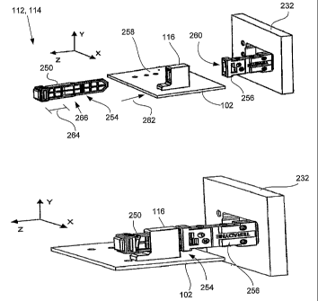
FIG. 6A shows a perspective view of the separable latching module 112, 1 I4
of FIGS. 4 and 5 along with a corresponding latching module 256 (also referred
to
herein as "receptacle member") on a printed circuit board 232, which is shown
as a
backplane. The separable latching module 112, 114 includes a guide member 250
and
a control assembly 254 which integrates with the guide member 250. The guide
to member 250 is configured to (i) slidably engage with the module support
member 116
attached to the daughter card 102 and (ii) selectively engage and disengage
with the
receptacle member 256. Accordingly, when the module support member 116 is
attached to the daughter card 102 and when the receptacle member 256 is
attached to
the backplane 232, the guide member 250 can latch the daughter card 102 to the
backplane 232 by engaging and locking with the receptacle member 256. Such
engaging and locking occurs when the guide member 250 is initially loaded
through
the opening 258 defined by the module support member 116, and then moved along
the Z-axis in the direction indicated by arrow 262 toward an opening 260
defined by
the receptacle member 256.
2o FIG. 6B shows the guide member 250 engaged with and locked to the
receptacle member 256. Accordingly, the daughter card 102 is now considered
latched to the backplane 232. In this situation, the guide member 250 is held
rigidly
by the receptacle member 256. Thus, any connecting elements rigidly attached
to the
guide member 250 and the receptacle member 256 can connect in a robust and
healthy
14
CA 02459290 2004-03-O1
WO 03/021320 PCT/US02/27474
manner. However, the guide member 250 is only loosely connected to the module
support member 116 in that there is Z-direction freedom of movement available.
The control assembly 254 is configured to retain the module support member
116 within a retaining range 264 of the guide member 250 when the guide member
250 is unlocked from the receptacle member 256. Such retention prevents the
guide
member 250 from inadvertently escaping from the module support member 116
prior
to latching and during the latching process. Additionally, the control member
254 is
further configured to un-restrict the module support member 116 such that the
module
support member 116 is movable outside of the retaining range 264 of the guide
to member 250 (i.e., movable to a location 266 outside the retaining range
264) when the
guide member 250 is locked with the receptacle member 256. It is this
operation that
provides for the desired float in the Z-axis.
A detailed discussion of the operation of the latching modules of FIGS. 4 - 6B
to provide Z-float can be found in a related application entitled "Techniques
For
15 Connecting A Set Of Connecting Elements Using An Improved Latching
Apparatus",
which is concurrently filed with the present application and which is
incorporated by
reference herein. It should be apparent to one of ordinary skill in the art
that because
of the modularity provided by the fiber optic connection system of FIGS. 4 and
5, the
fiber optic connection system of the present invention is not limited in its
20 configuration by the number of separable wafer modules, number of separable
latching modules, number of optical fibers required or other such
considerations.
Deferring now to FIGS. 7 and 8, there are shown an alternate embodiment of a
carrier design for separable wafer modules and latching modules, where the
carrier is
designed to provide easy addition/removal of the wafer modules. The carriers,
which
25 axe generally shown by reference numerals 300 and 320, can hold the
separable wafer
CA 02459290 2004-03-O1
WO 03/021320 PCT/US02/27474
modules and latching modules of FIG. 2, or the separable wafer modules and
latching
modules of FIGS. 4 - 6B. In FIGS. 7 and 8, the carriers 300, 320 preferably
hold the
wafer modules 110 and the latching modules 256 of the backplane 232.
The Barrier 300 is shown having an opening 301 for receiving a separable
wafer module 110. The carrier 300 also includes a first tab 302 having first
and
second apertures 303a, 303b and a second tab 304 having an aperture 305. The
carrier 320 is shown having an opening 321 with slots provided therein to
receive
three separable wafer modules 110. The carrier 320 also includes a first tab
322
having first and second apertures 323a, 323b and a second tab 324 having an
aperture
325.
Latching modules 256 are provided with engagement means configured to
engage the apertures 303a, 303b, 305, 325, 323a, 323b in the tabs of the
carriers 300,
320 to attach the Latching modules to the carriers. For example, the
engagement
means may be protrusions which, in FIG. ~, are attached by rivets 310 or the
like.
Preferably, each latching module 256 has two protrusions corresponding to the
two
apertures available for each latching module. However, it should be apparent
to one
of ordinary skill in the art that any number of apertures and protrusions may
be
available for the carrier and latching module, respectively, without departing
from the
scope of the present invention.
The second tab 304 of the carrier 300 and the second tab 324 of the carrier
320
are preferably positioned adjacent one another when the carriers are attached
to the
backplane 232 such that a separable latching module 256 may be attached
between
the carriers 300, 320 without wasting backplane space. Another advantage of
the
carriers 300, 320 is the simplicity in adding/removing any of the separable
wafer
modules 110 from the carriers. This can be accomplished, for example, by
providing
16
CA 02459290 2004-03-O1
WO 03/021320 PCT/US02/27474
an actuable mechanism (not shown) on the carriers 300, 320. The separable
wafer
modules 110 can also be provided with separable ferrule assemblies 180, which
may
utilize actuable clips 170 or the like, for engaging/disengaging the ferrule
assembly
from the wafer module housing.
~y providing a limited number of carriers of the present invention with
openings configured for different numbers of separable wafer modules (for
example,
providing carriers for holding 2, 3 and 4 wafer modules), the fiber optic
connection
system of the present invention can be made to accommodate a wide variety of
system
configurations without the expenses associated with the prior art.
l0 Having described the preferred embodiment and alternative embodiments of
the invention in sufficient detail to enable those skilled in the art to make
and use the
invention, it will nevertheless be appreciated that variations and
modifications to the
described embodiments may be made without departing from the spirit and scope
of
the invention, and it is intended that the invention not be Limited to the
above
15 description or accompanying drawings, but that it be defined in accordance
with the
following claims.
17