Note: Descriptions are shown in the official language in which they were submitted.
CA 02459545 2004-02-26
WO 2004/010283 PCT/US2003/021164
METHOD AND APPARATUS FOR PROVIDING A SUPPLY VOLTAGE
BASED ON AN ENVELOPE OF A RADIO FREQUENCY SIGNAL
Field of the Invention
The present invention relates generally to wireless communication devices and
in particular to a wideband envelope tracking amplification system of a
wireless
communication device.
Background of the Invention
Power amplifiers for wireless transmission applications, such as radio
frequency (RF) power amplifiers, are utilized in a wide variety of
communications
and other electronic applications. Ideally, the input-output transfer function
of a
power amplifier should be linear, that is, should implement a constant gain
adjustment
and phase adjustment of an input signal, wherein a perfect replica of the
input signal,
increased in amplitude, appears at the output of the power amplifier.
In addition, for greater efficiency, various RF systems, such as cellular
systems, attempt to run power amplifiers at or near their saturation levels,
in which
the actual output power of the amplifier is just below its maximum rated power
output
level. This power output level is generally related to the supply voltage (or
supply
power) to the power amplifier, such that a greater supply voltage will produce
a
correspondingly greater output power from the amplifier; for higher power
input
signals, a correspondingly greater actual power output is required to maintain
the
amplifier at or near saturation. In various prior art amplifiers, however, the
supply
voltage to the power amplifier is fixed. Given a typical usage , situation in
which
actual power output from the amplifier may vary by a range of several orders
of
magnitude, use of a fixed supply voltage is highly inefficient, as output
power is often
an order of magnitude or more below its maximum, and the power amplifier is
not
maintained at or near its saturation levels.
CA 02459545 2004-02-26
WO 2004/010283 PCT/US2003/021164
2
Various techniques have evolved to vary the supply voltage to maintain the
power amplifier at or near saturation. One such technique is power supply
modulation (PSM) that varies, or modulates, the supply voltage to the power
amplifier
in order to maintain the power amplifier at or near saturation while the input
signal
varies over time. For PSM, the supply voltage of the amplifier tracks the
input signal
variations, typically utilizing a signal detector in conjunction with a
tracking power
supply. In the prior art, however, the various PSM techniques have generally
been
limited to narrowband applications, or have poor efficiency characteristics.
For example, one prior art PSM technique, known as "envelope elimination
and restoration" (EER), utilizes a limner to provide an essentially constant
drive level
to the power amplifier to maintain the amplifier in a hard saturation state
and increase
efficiency. Use of the limiter, however, greatly expands the bandwidth of the
RF
signal input to the amplifier and requires very accurate tracking of the input
signal
envelope, with a power supply switching frequency approximately ten times
greater
than the bandwidth of the RF input signal. As these switching frequencies
increase,
the transistors within the tracking power supply become less efficient,
resulting in
excessive power losses. The resulting bandwidth expansion of the limiter also
requires the bandwidth capability of the amplifier to be significantly greater
than the
input signal bandwidth, limiting the EER configuration to narrow bandwidth
applications, such as amplitude modulation (AM) RF broadcasts.
Another prior art PSM technique, known as "envelope tracking," does not
utilize the limiter of EER. Consequently, envelope tracking power
amplification
systems may be more suitable for higher bandwidth applications. FIG. 1 is a
block
diagram of an exemplary envelope tracking power amplification system 100. A
radio
frequency (RF) signal 101 is coupled to an input 102 of amplification system
100. A
signal coupler 104 samples input signal 101 to produce a sampled input signal
105
and routes sampled input signal 105 to an envelope tracking power supply
(ETPS)
106. ETPS 106 tracks or detects an envelope of sampled input signal 105 to
produce
an envelope detector signal, typically a voltage, and produces a variable
supply
voltage 107 based on the detected envelope of input signal 101. ETPS typically
CA 02459545 2004-02-26
WO 2004/010283 PCT/US2003/021164
3
includes a switching power supply whose switching pulse width or frequency is
varied in order to track the envelope of input signal 101 and produce variable
supply
voltage 107.
ETPS 106 sources variable supply voltage 107 to an RF power amplifier 108.
Variable supply voltage 107 is designed to maintain RF power amplifier 108 at
or
near saturation and to increase the efficiency of power amplification system
100 over
a wide range of variation in input signal 101. When input signal 101 is a
wideband
RF signal, the switching power supply of ETPS 106 must have a very rapid
response
in order to track RF input signal 101. However, if variable supply voltage 107
is to
accurately reproduce the envelope of RF input signal 101, then the switching
frequency of ETPS 106 should be 5-10 times the bandwidth of input signal 101.
For
example, if input signal 101 has a bandwidth of 20 MHz, as is common in multi-
carrier amplification systems, then ETPS 106 should have a prohibitively high
switching frequency of 100-200 MHz.
In order to resolve the requirement for a prohibitively high switching
frequency power supply, schemes have been proposed for utilizing multiple
voltage
supplies in implementing the ETPS, such as in U.S. patent no. 5,239,275,
entitled
"Amplitude Modulator Circuit Having Multiple Power Supplies," and U.S. patent
no.
5,736,906, entitled "Power Supply Modulator Circuit for Transmitter." Such
schemes
typically involve selecting a voltage supply of the multiple voltage supplies,
or
serially connecting one or more voltage supplies of the multiple voltage
supplies,
based on a detected instantaneous magnitude, or amplitude, of the input
signal.
However, mufti-carrier input signals typically have a wide dynamic range,
often in the
range of 10-20 dB, due to high short-term peak-to-average power ratios caused
by the
multiple carriers and due to long term fluctuations in average power due to
variations
in traffic loading. In order to track a mufti-carrier input signal, the ETPS
may require
a subdivision of an input signal voltage range into as many as 10 to 12 input
signal
amplitude steps and correspondingly may require as many as 10-12 voltage
supplies.
The use of such a large number of voltage supplies is both prohibitively
expensive
and complex.
CA 02459545 2004-02-26
WO 2004/010283 PCT/US2003/021164
4
Therefore, there is a need for a high efficiency, low cost method and
apparatus
for tracking a wideband RF signal under high dynamic range conditions.
Brief Description of the Drawings
FIG. 1 is a block diagram of an envelope tracking amplification system of the
prior art.
FIG. 2 is a block diagram of an envelope tracking amplification system in
accordance with an embodiment of the present invention.
FIG. 3 is a block diagram of the envelope tracking power supply of FIG. 2 in
accordance with an embodiment of the present invention.
FIG. 4 is a logic flow diagram of steps executed by the envelope tracking
amplification system of FIG. 2 in amplifying a radio frequency signal in
accordance
with an embodiment of the present invention.
Detailed Description of the Invention
To address the need for a high efficiency, low cost method and apparatus for
tracking a wideband RF signal under high dynamic range conditions, an envelope
tracking amplification system that includes an envelope tracking power supply
(ETPS) amplifies a radio frequency (RF) signal to produce a linearized
amplified
signal. The envelope tracking amplification system samples the RF signal to
produce
a sampled RF signal. The ETPS produces a control signal based on an
instantaneous
magnitude of the sampled RF signal and further based on an average magnitude
of the
sampled RF signal, produces multiple supply voltages, and, based on the
control
signal, couples a supply voltage of the multiple supply voltages to an output
of the
EPTS to produce an output supply voltage. The envelope tracking amplification
system then amplifies the RF signal based on the output supply voltage to
produce a
highly linear amplified signal.
Generally, one embodiment of the present invention encompasses an apparatus
for controlling a supply voltage output by an envelope tracking power supply.
The
CA 02459545 2004-02-26
WO 2004/010283 PCT/US2003/021164
S
apparatus includes a first detector that detects a magnitude of a radio
frequency (RF)
signal and produces a first detector signal corresponding to an average
magnitude of
the RF signal and a second detector that detects a magnitude of the RF signal
and
produces a second detector signal corresponding to an instantaneous magnitude
of the
RF signal. The apparatus further includes a ratioing unit coupled to each of
the first
detector and the second detector that compares the first detector signal to
the second
detector signal to produce a comparison and produces a control signal based on
the
comparison, wherein the control signal is capable of controlling a supply
voltage
output by the envelope tracking power supply.
Another embodiment of the present invention encompasses a method for
controlling a supply voltage output by an envelope tracking power supply. The
method includes steps of detecting a first magnitude of an RF signal to
produce a first
detected magnitude and, based on the first detected magnitude, producing a
first
detector signal corresponding to an average magnitude of the RF signal. The
method
further includes steps of detecting a second magnitude of the RF signal to
produce a
second detected magnitude and, based on the second detected magnitude,
producing a
second detector signal corresponding to an instantaneous magnitude of the RF
signal.
The method further includes steps of comparing the first detector signal to
the second
detector signal to produce a comparison and producing a control signal based
on the
comparison, wherein the control signal is capable of controlling a supply
voltage that
is output by the envelope tracking power supply.
Yet another embodiment of the present invention encompasses an envelope
tracking amplification system for amplifying an RF signal. The envelope
tracking
amplification system includes a signal coupler that samples the RF signal to
produce a
sampled RF signal and an envelope tracking power supply operably coupled to
the
signal coupler and having an input and an output, wherein the envelope
tracking
power supply receives the sampled RF signal at the input, produces a control
signal
based on an instantaneous magnitude of the sampled RF signal and further based
on
an average magnitude of the sampled RF signal, produces a plurality of supply
voltages, and, based on the control signal, couples a supply voltage of the
plurality of
CA 02459545 2004-02-26
WO 2004/010283 PCT/US2003/021164
6
supply voltages to the output to produce an output supply voltage. The
envelope
tracking amplification system further includes an RF power amplifier operably
coupled to the envelope tracking power supply that receives the output supply
voltage
and amplifies the RF signal based on the output supply voltage to produce an
amplified signal.
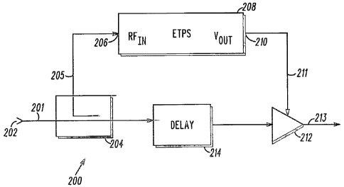
The present invention may be more fully described with reference to FIGs. 2-
4. FIG. 2 is a block diagram of envelope tracking amplification system 200 in
accordance with an embodiment of the present invention. Envelope tracking
power
amplification system 200 includes an input 202 operably coupled to a signal
coupler
204, preferably a directional coupler, and further operably coupled to an RF
power
amplifier 212 via signal coupler 204 and a delay circuit 214. Envelope
tracking
power amplification system 200 further includes an envelope tracking power
supply
(ETPS) 208 that is operably coupled at an input 206 to signal coupler 204 and
at an
output 210 to RF power amplifier 212. Delay circuit 214 is utilized to delay,
and
thereby synchronize, a version of input signal 201 that is applied to RF power
amplifier 212 with a corresponding variable supply voltage 211 that is sourced
by
ETPS 208 to the RF power amplifier. RF power amplifier 212 includes an RF
amplifying element, an input matching circuit, an output matching circuit, and
biasing
and decoupling circuitry as are necessary to allow the functionality of the RF
amplifying element and to bias the RF amplifying element class AB; however,
those
of ordinary skill in the art realize that other biases, such as classes A, B,
or C, may be
used here without departing from the spirit and scope of the present
invention.
When an RF signal 201 is coupled to input 202 of amplification system 200,
the amplification system routes the RF signal to signal coupler 204. Signal
coupler
204 samples input signal 201, to produce a sampled input signal 205 and routes
the
sampled input signal to ETPS 208 via ETPS input 206. ETPS 208 detects, or
tracks;
the envelope of input signal 201 and produces a variable supply voltage 211
based on
the envelope of input signal 201. ETPS 208 then sources variable supply
voltage 211
to RF power amplifier 212 via ETPS output 210. RF power amplifier 212
amplifies a
delayed version of input signal 201 based on variable supply voltage 211 to
produce
CA 02459545 2004-02-26
WO 2004/010283 PCT/US2003/021164
an amplified signal 213 that is output by amplification system 200. By
detecting, or
tracking, the envelope of input signal 201, ETPS 208 provides a variable
supply
voltage 211 to RF power amplifier 212 that enables the RF power amplifier to
be
maintained at or near saturation over a wide range of magnitudes of input
signal 201,
thereby providing for highly efficient amplification of the input signal.
FIG. 3 is a block diagram of ETPS 208 in accordance with an embodiment of
the present invention. ETPS 208 includes an average envelope detector 302, a
fast
envelope detector 304, and a ratioing unit 306 operably coupled to each of the
average
envelope detector and the fast envelope detector. ETPS 208 further includes
multiple
tracking power supplies 310-312 (three shown) that are each operably coupled
to the
average envelope detector 302 and a switching device 314 operably coupled to
ratioing unit 306, to each power supply of the multiple tracking power
supplies 310-
312, and to output 210 of ETPS 208. In order to accurately reproduce the
envelope of
RF input signal 201 when the signal is a wideband signal with a wide dynamic
range,
ETPS 208 produces a variable supply voltage 211 that is based on both an
instantaneous magnitude and an average magnitude of input signal 201. By
utilizing
both the instantaneous magnitude and the average magnitude of input signal 201
in
producing variable supply voltage 211, ETPS 208 is able to accurately
reproduce the
envelope of RF input signal 201 under wide dynamic range conditions at a lower
cost
and complexity than the prior art.
FIG. 4 is a logic flow diagram 400 of steps executed by envelope tracking
amplification system 200 in amplifying RF input signal 201 in accordance with
an
embodiment of the present invention. Logic flow diagram 400 begins (402) when
RF
signal 201 is coupled (404) to input 202 of system 200. Envelope tracking
amplification system 200 routes input signal 201 to signal coupler 204. Signal
coupler 204 samples (406) input signal 201 to produce sampled input signal
205.
Signal coupler 204 then routes sampled input signal 205 to ETPS 208.
ETPS 208 routes at least a first portion of sampled input signal 205 to
average
envelope detector 302 and at least a second portion of sampled input signal
205 to fast
envelope detector 304. The at least a first portion and the at least a second
portion of
CA 02459545 2004-02-26
WO 2004/010283 PCT/US2003/021164
g
sampled input signal 205 may be identical signals. Average envelope detector
302
detects (40g), or tracks, a magnitude of the at least a first portion of the
sampled input
signal over a suitable period of time, such a 10 microseconds (~.s). Based on
the
detected magnitude, average envelope detector 302 produces (410) a first
envelope
detector signal 303, typically a voltage (VAVG), that corresponds to the
magnitude of
the at least a first portion of sampled input signal 205 averaged over, the
period of
time. Average envelope detector 302 then conveys first envelope detector
signal 303
to ratioing unit 306 and to each of the multiple tracking power supplies 310-
312.
In one embodiment of the present invention, average envelope detector 302
may comprise a first diode detector that is coupled at its output to a first
low pass
filter. Preferably the low pass filter has a cutoff that is well below the
frequency of
RF input signal 201, such as a cutoff that filters out all signals above the
audio band.
In another embodiment of the present invention, average envelope detector 302
may
comprise the fast envelope detector 305 described below followed by yet
another low
pass filter with a suitable cutoff band. Those who are of ordinary skill in
the axt
realize that there axe many techniques for implementing an average envelope
detector
that produces a signal that corresponds to an average, over some suitable
period of
time, of a magnitude of a signal coupled to the detector, and that any such
technique
may be used herein without departing from the spirit and scope of the present
invention.
Based on first envelope detector signal 303, each tracking power supply of the
multiple tracking power supplies 310-312 produces (412) a variable supply
voltage
that is proportional to the first envelope detector signal but is at a
different voltage
level than the variable supply voltages produced by the other power supplies
of the
multiple tracking power supplies 310-312. For example, power supply 310 may be
a
low voltage (VLOW) power supply. Power supply 311 may then be a mid-range
voltage (VMID) power supply, such as a power supply with a maximum output
voltage
that is two times the maximum output voltage of power supply 310, and power
supply
312 may be a high voltage (VHI) power supply with a maximum output voltage
that is
four times the maximum output voltage of power supply 310. Preferably, the
scaling
CA 02459545 2004-02-26
WO 2004/010283 PCT/US2003/021164
9
between first envelope detector signal 303 and the output voltages of each of
the
multiple power supplies 310-312 is such that the maximum output voltage of the
top
voltage range (VHI) power supply, that is, power supply 312, is attained when
first
envelope detector signal 303 attains a magnitude corresponding to the maximum
average RF power rating of envelope tracking amplification system 200. For
example, if the RF amplifying element of RF power amplifier 212 is a lateral
drain
metal oxide semiconductor (LDMOS) with a voltage rating of 26 volts (V), then
the
maximum output voltage of power supply 312 may be 26V and the maximum output
voltages of power supplies 311 and 310 may be 13V and 6.5V, respectively.
Fast envelope detector 304 detects (414), or tracks, a magnitude of the at
least
a second portion of sampled input signal 205 and, based on the detected
magnitude,
produces (416) a second envelope detector signal 305, typically a voltage
(V~sT), that
corresponds to an instantaneous magnitude of the at least a second portion of
sampled
input signal 205. Fast envelope detector 304 then conveys second envelope
detector
signal 305 to ratioing unit 306.
In one embodiment of the present invention, fast envelope detector 304 may
comprise a second diode detector that is coupled at its output to a second low
pass
filter. Preferably the second low pass filter cuts off at a higher frequency
than the
cutoff of the first low pass filter but that is also well below the frequency
of RF input
signal 201, such as a low pass filter with a passband that is approximately as
wide as
the bandwidth of the envelope of RF input signal 201. Those who are of
ordinary
skill in the art realize that there are many techniques for implementing a
fast envelope
detector that produces a signal that corresponds to an instantaneous magnitude
of a
signal coupled to the detector, and that any such technique may be used herein
without departing from the spirit and scope of the present invention.
Preferably, ratioing unit 306 is implemented in a processor, such as a
microprocessor, a digital signal processor (DSP), or a microcontroller, and
further
includes multiple analog-to-digital converters (A/D's) that digitize each of
signals 303
and 305 to produce digital signals that are processed by the processor.
Ratioing unit
306 may further include a digital-to-analog converter (D/A) that produces an
analog
CA 02459545 2004-02-26
WO 2004/010283 PCT/US2003/021164
control signal 307 when switching device 314 is an analog signal-controlled
device.
Ratioing unit 306 receives first envelope detector signal 303 from average
envelope
detector 302 and fixrther receives second envelope detector signal 305 from
fast
envelope detector 304. Ratioing unit 306 produces (418) a control signal 307
based
5 on first envelope detector signal 303 and second envelope detector signal
305 and
conveys the control signal to switching device 314. Based on control signal
307,
switching device 314 then couples (420) a tracking power supply of the
multiple
tracking power supplies 310-312 to output 210 of ETPS 208, thereby coupling
the
supply voltage produced by the coupled tracking power supply to output 210 to
10 produce ETPS output supply voltage 211.
Envelope tracking amplification system 200 routes ETPS output supply
voltage 211 to RF power amplifier 212. In addition to receiving output supply
voltage 211, RF power amplifier 212 receives a delayed version of input signal
201
from signal coupler 204 via delay circuit 214. RF power amplifier 212
amplifies
(422) the delayed input signal 201 based on output supply voltage 211 to
produce
amplified signal 213, and the logic flow ends (424).
Preferably, the step of producing control signal 307 includes steps of
comparing first envelope detector signal 303 to second envelope detector
signal 305
to produce a comparison and producing the control signal based on the
comparison.
Preferably, the step of comparing first envelope detector signal 303 to second
envelope detector signal 305 comprises a step of determining a ratio of second
envelope detector signal 305 to first envelope detector signal 303 (herein
referred to
as the "lNSTIAVG" ratio). Ratioing unit 306 then produces control signal 307
based
on the determined ratio. However, those of ordinary skill in the art realize
that other
methods of comparing first envelope detector signal 303 to second envelope
detector
signal 305 may be used herein without departing from the spirit and scope of
the
present invention. For example, ratioing unit 306 may determine a ratio of
first
envelope detector signal 303 to second envelope detector signal 305 (an
AVG/INST
ratio) or may determine a difference between second envelope detector signal
305 and
first envelope detector signal 303.
CA 02459545 2004-02-26
WO 2004/010283 PCT/US2003/021164
11
In one embodiment of the present invention, switching device 314 comprises a
multiplexer that includes an output coupled to output 210 of ETPS 208 and
multiple
inputs that are each coupled to a tracking power supply of the multiple
tracking power
supplies 310-312. Control signal 307 may then be a voltage whose magnitude is
varied based on the comparison determined by ratioing circuit 306 of first
detector
signal 303 to second detector signal 305, such as a voltage that is
proportional to the
INST/AVG ratio. Based on the magnitude of control signal 307, switching device
314 couples an input of the multiple multiplexer inputs to the multiplexer
output,
thereby coupling a corresponding tracking power supply to output 210 of ETPS
208.
Preferably, the coupled power supply is capable of sourcing a voltage in a
voltage
range that is sufficient to keep the RF amplifying element of RF power
amplifier 212
at or near saturation without causing clipping when the RF amplifying element
amplifies the corresponding input signal 201.
In another embodiment of the present invention, switching device 314 may
comprise multiple switching devices, such as PIN diodes or GASFET switches,
that
axe each closed or opened, or enabled or disabled, by a control signal
received from
ratioing unit 306. Each switching device of the multiple switching devices is
coupled
at an output to a signal combiner and at an input to a tracking power supply
of the
multiple tracking power supplies 310-312. In addition, each switching device
is
individually coupled, for example by a set of logic lines, to ratioing unit
306. Control
signal 307 may then comprise one or more control signals, wherein each control
signal of the one or more control signals is used by ratioing unit 306 to
close or open a
corresponding switching device, thereby respectively coupling a corresponding
tracking power supply to or decoupling a corresponding tracking power supply
from
output 210 of ETPS 208. In such an embodiment, the step of producing (416) a
control signal 307 may include the following steps. Ratioing unit 306 compares
the
ratio or difference determined with respect to the first and second envelope
detector
signals 303, 305 to at least one threshold, which the at least one threshold
is stored in
a memory associated with the processor implementing the ratioing unit.
Ratioing unit
306 utilizes the at least one threshold to determine which tracking power
supply of the
multiple tracking power supplies 310-312 to couple to output 210 of ETPS 208.
CA 02459545 2004-02-26
WO 2004/010283 PCT/US2003/021164
12
Based on the comparison of the determined ratio or difference to the
threshold,
ratioing unit 206 produces a control signal 307 which causes an appropriate
power
supply of the multiple power supplies 310-312 to be coupled to output 210.
For example, and merely for the purpose of illustrating the principles of the
present invention, ratioing unit 306 may cause switching device 314 to couple
power
supply 310 to output 210 when an INST/AVG ratio determined by the ratioing
unit is
less than one (1). When the INST/AVG ratio is between one (1) and two (2)
(i.e., a
ratio of 0 to 6 dB), ratioing unit 306 may cause switching device 314 to
couple power
supply 311 to output 210, and when the INST/AVG ratio greater than two (2),
ratioing
unit 306 may cause switching device 314 to couple power supply 312 to output
210.
Such a scheme would prevent RF power amplifier 212 from clipping a signal
amplified by the amplifier for INST/AVG ratios of up to 4 (i.e., a ratio of 12
dB).
In sum, an envelope tracking amplification system 200 is provided that
includes an envelope tracking power supply (ETPS) 208 and that amplifies an RF
signal 201 coupled to the system to produce a linearized amplified signal. A
signal
coupler 204 included in the envelope tracking amplification system samples the
RF
signal to produce a sampled RF signal 205. ETPS 208 produces a control signal
307
based on an instantaneous magnitude of the sampled RF signal and further based
on
an average magnitude of the sampled RF signal. ETPS 208 further produces
multiple
supply voltages, and, based on the control signal, couples a supply voltage of
the
multiple supply voltages to an output 210 of the EPTS to produce an output
supply
voltage 211. Envelope tracking amplification system 200 then amplifies RF
signal
201 based on output supply voltage 211 to produce a highly lineax amplified
signal
213. By producing a control signal that controls ETPS output supply voltage
211
based on both an instantaneous magnitude and an average magnitude of the
sampled
RF signal, while producing multiple supply voltages based on the average
magnitude
of the sampled RF signal, envelope tracking amplification system 200 is able
to
accurately reproduce the envelope of a wideband RF signal under wide dynamic
range
conditions in a highly efficient and low cost manner.
CA 02459545 2004-02-26
WO 2004/010283 PCT/US2003/021164
13
While the present invention has been particularly shown and described with
reference to particular embodiments thereof, it will be understood by those
skilled in
the art that various changes may be made and equivalents substituted for
elements
thereof without departing from the scope of the invention as set forth in the
claims
below. Accordingly, the specification and figures are to be regarded in an
illustrative
rather then a restrictive sense, and all such changes and substitutions are
intended to
be included within the scope of the present invention.
Benefits, other advantages, and solutions to problems have been described
above with regard to specific embodiments. However, the benefits, advantages,
solutions to problems, and any elements) that may cause any benefit,
advantage, or
solution to occur or become more pronounced are not to be construed as a
critical,
required, or essential feature or element of any or all the claims. As used
herein, the
terms "comprises," "comprising," or any variation thereof, are intended to
cover a
non-exclusive inclusion, such that a process, method, article, or apparatus
that
comprises a list of elements does not include only those elements but may
include
other elements not expressly listed or inherent to such process, method,
article, or
apparatus.