Note: Descriptions are shown in the official language in which they were submitted.
CA 02459660 2004-03-04
~I-I EL~ ~Dh E.~P PI~~'EI~ CI "~1EL I~NlfT~I1, EM~IoC?'YII~
-ID ~I~ISIf~PII'~~1VI~ E.'Y~;T
E1~CI~GE .t~LT~TD ~E SHE I~ N'~I~il'
Field of the Invention
The present invention. relates to channel ad~ldrop filters and channel
m~nitors employing photo ~~c crystals, and in par~ic~~ to improvements in the
adaptability of such channel add/drop filters and channel monitors to
polarized
waves.
i~ It should be understood that in the present spc~°~ 'ca.tion, the si
cants
of the term '°light" is meant to also include electromagnetic waves
that relative
t~ visible light are of longer as well as shorter waveh~ath.
Description of the ac~ground art
l~l.ong with advances in wavelength division multiplexed optical
t5 com~.unicati.on systems recent ye s, the ~ porta~ce of optical devices such
as adthdrop filters, channel. filters, and charnel a~xo~itors is on the rose.
In
addition, °aturization of these es of optical dew~.ces is being sought.
If for
ex ple a ,wavelength mo ~tor were to be pro~~ded for each of optical
amplihersltransponders in an optical com~nu~catior~ system, the wavelength
2~ monitor would have to be stalled on the optical tr sponder platform. F3ut
because wavelength no.onators currently bey~ag used are large, in.st g them on
the platforms is physically impossible. ~'hus owing to the need for
'aturazation of optical de~~ces, photonic crystals ~~e ~~eing used in attempts
CA 02459660 2004-03-04
2
to develop extraor ~ ' gy sm -scale optical devices,. In particular, e~ith
photonic crystals extremely s~ al3-scab: optic device:9 can be ~°e ed
by
exploiting artificial periodic structures iu. which a crystal-lattmce-l:'~e
periodic,
ultra-dense refractive index distribution. is cially imparted within the
parent material.
~ne important feature of plxotonic crystals is the presence of photonic
bandgaps. V~7'ith photonic ~:rystals ba~iing tree-dimensional refractive index
periodicity (317 photonic crystals), perfect bandgaps which the tra.ns~ission
of light is prohibited every direction can be forr~eei_ Elxnong the
possibilities
~.0 with these crystals are tb a local co nement of light, control of
spo~ataneous
emission, and formation of ~ravegc~ies by the i.~.trociuction of a defects,
wherein the realg~ation of ul.trasmall photonic integrated circuits is
anticipated.
ll~eanw ~ e, studies into uses for pb otonic ci°y:~tals b a ' g a two-
dimensional. periodic refractive-index structure (~17 ,~botonic crystals), are
I~ flourishing because the crystals can be ~.anufactured comparatively easily
A
periodic refractive-index structure in X17 photonic crystals can be foxed by,
fox
example, arranging in a square-lattice or triang~zlar-lattice geometry air
rods
perforating a high-refractive-index plate material (usually termed a "'slab").
Alternatively the structure can ~be formed within a low-index material by
2Q arranging, in a 2I)-latce geoHnetry wi it, posts xnasle of a high-
ref~active-
index material. I'hotonic bandgaps can. be produced frown. such periodic
refractive-index structures, r~r~abli~ag the ~;:~ansxnissi~on of laght Crave '
g in an
in-plane direction (direction parallel to both tl~e princ:ipa7i feces of the
slab) to be
CA 02459660 2004-03-04
controlled. ~Vaveguides, for instance, may be created by introducing lice
defects
iuto a periodic refractive-~de~ structure. ( ice, for e~ plc,
.T'~y~zc~'evaerrr.~,
V'ol_ ~2, 2U0~, pp. 448-~4~~~.~
Fig. 5 illustrates, ~. a scheatYC oblique viewu, a channel addldrop filter
disclosed in Japanese ~.~uea~ ed Pat. App. Pub. PTO. 20a3-2°12555. (In
the
drags i~ the present application, identical referf~nce mars i_~.dacate
identical or equivalent part:y.} The ch el addfdrop ester :gin Fig. 5 exploits
a 2I~
photonic crystal having, cor~.fgured writ ° a slab 1, cylindrical
through-boles 2
of identical diameter (or ' arily occupied by air) fo~~.ed at the vertices of
a 2~
triangular lattice. In a ~I~ photord.c cr~rstal of this sort, light is
prohibited f~oaa~
propagating in an ~.-plane ~lirectio~a within the slab by a bandgap, aid in
the
direction a~ormal to the plane ( ° eetiou orthogonal t;o the two
principal faces of
the slabs is confined due to total ' ternal reflection. occurring at the
interface
with the low-rei~active-i.n dex clad ( ° , for ex plc).
t.5 The photonic crystal in Fig. 5 contains a w;~~re~,.e 3 consisting of a
straight line defect. This straight- ° a defect 3 includes a :sec '
early rain ° g
plurality of lattice poiaits ad~o° g each other, vrith the through-
holes 2 °ssing
iai these lattice points. 9~ith light being able to propagate through a defect
in a
~I3 photonic crystal, the straight- ' a defect can be employed as a linear
waveguide. With linear waveguiides, the spectrum of wavelengths an which light
can be transmitted at lour loss is comparatively broad; consequently light in
a
wide range of wavelength co~tai~ng sigaaals ba a phurality of chan~.els naay
be
propagated through thean.
CA 02459660 2004-03-04
The photonic crystal set out in Fig. ~ also cont° ' .s a cavity 4
co~asisting of
a povnt defect. The point defect ~ cant ' s a singh' lai;tir:e point, and
through
that lattice point a through-hole that is of large diameter as compared vnith
the
other lattice points is for~~ed. ~3 defect in this Amy cant ' g a relatively
large-diameter through-hole is generally termed a~~ acc:eptor-type point
defect.
~n the other hand, a defect in which through-holes are : 'ssi~ag in lattice
points
is generally termed a door-type point defect. a cavity ~~ is disposed adjacent
the waveg~zide 3, within a range in ~~vhich they can exert on each other an
electromagnetically recipro~:al effect.
1~ In a ~I3 plsotonic cr~rstal such as that illustrated in Fig. 5, if light 5
coat ' g a plurality of waeaelength ranges (~.1, ~,~, _ . . ~." . . .~ is
introduced into
the waveg~aide 3, light that has the specific wavelength ~.; correspon
° g to the
resonant frequency of the cavity ~ is trapped in the cavity and ~crhile
vesonating
in flee interior of the point defect, light f~ of wavelength ~,, is emitted in
the
~ 5 plane-normal direction, in which due to the Emits thi ess of the slab ~
the ~
factor is small_ This means ;hat the photonic crystal in Fig. ,~ can be
employed
as a channel drop filter. Conversely, by s ° g light into the point
defect 4, in
the direction normal to the slab I, light of wavelength ~'a that resonates
within
the cavity 4 can be introduced into the waveguide d. This means that the
2~ photonic crystal in Fig_ 5 can also be employed as a channel add filter. It
wall be
appreciated that the transfer of light between either the wavegui.de 3 or the
cavity 4 and the exterior can be made to tale place by pro~.mately disposing
axe
optical. fiber or an optoelectronic transd~xcer in the vici~.ity of the
waveguide end
CA 02459660 2004-03-04
faces or the vicinity of the; cavity. C~f course, in that case a co ' sting
lens
(collimator) array be inserted in between either the wave °de end face
or the
cavity, and the optical-fiber end face or tb.e optoelectronic transducer.
In an optical addfdrop fxlter such as that illustrated in ~'ig. 5, by
appropriately con~.guring the spacing between the waveguide 3 consisting of
the hne defect and the cavity ~ con.sist~g of the point defect, the ratio of
optical
intensities i:n. a speci~'cc wavelength that is transferred between the
waveguide
and the cavity can be controlled. .E~Lso in Wig. 5, since no asymmetry is
introduced with respect to the point defect ~ in the ' ectic~n normal to the
slab
1, Light is output in both vertical. directions frog the point defect 4y but
it is
possible t~ make the output of light be in only one o:~ the other vertical
direction
by introducing asyxnn'.etry in the point defect ~ in the plane-normal
direction°
~n example of a mechanism that can be a ° ' ed. to introduce this sort
of
asyxuxnetry is a method in which the diameter of tb.e point defect ~, which is
round in section, is made to vary continuously or discontinuously along the
thickness of the slab_ kith er regard to dig. 5, although the channel
add/drop .ter in the ~g~zre contains only a single cavity, it will be readily
understood that by disposing along the waveguide a plurality of cavities
eying from one another resonant wavelength, op~cical signals in a plurality
of channels can be addedldropped. It be appreciated that the resonant
wavelength of the cavity ~ can be changed by, for ff'~~~nple, altering the
dianensionsishape of the point defect.
~'he fact that, as described above, a channel addo'dro7,~ alter such as that
CA 02459660 2004-03-04
6
depicted in dig. 5 ~aal~es it possible to ewtract as lig~t ~ light of a sp~c.c
wavelength ~., oily---co~.t ° cd 't ' ~~ o~t~cal si~;a~~l 5-a the
ca~aty ~
pans that the filter gay be c~aloyed ~ravolen~;~b otors.
~,efere~ce is jade to dig. ~, which scbeatic~lly illustrates an oblique
~ v-iew one ex ple of a ~veleugtl°~ motor e~aplcaw ' g c~ 2~ photonic
crystal
such as just discussed. ~"hree cavities 4a, 4b d 4c ~ egg frog one another
resonant frequency are Iarovided in this vvavelen,gth rr~oa~.tor, and adjacent
to
these cavities the end faces, of optical ~.bers I~a, IOb a~~IOc are disposed
so as
to a it the light of the slaecic freque~a.cies radiated frog the cavities.
These
t0 optical fibers are in t~xrr~ co acted ts~ photoele4aric serasir~g eleewts
(not
ill~.stratedj, wherein the specific frequencies of ~.i~bt are detected by the
photoelectric sensing ale esnts.
nevertheless, in a ch el add/droalter en~p~.oying a 21~ photonic
crystal such as illustrated i:a dig. 5, wit ' the light oaf t:be specific
wavelength ~,1
I5 only that portion evbose electric-held vector bas a component par el to the
p ' cipal plane of the ~pbotonic crystal I c a e:a~tra.cta'd frog the cavity 4
as
emitted light . ~n the other h d, the Iigt 5, ~rl.cll~ i_s introduced unto the
wave °de 3 by, for e~ ple, optical fiber, . at es be pal ed in a
speck direction by the optical fiber or by the ii~nact of the en ' anent
2~ lea ° g up to it. for inst ce, a situation where tb.e electric-held
vector of the
light cf waveler~gtb ~., cant ° ed the a.~.troduced Iight 5 is pal ed
perpendica~la~ to the princilaal pl a of the 2f7 pbotcan~c crystal I ' ~ mean
that
light of wavelength ~,, c of be onitored using the cha~~nel add/drop alter of
CA 02459660 2004-03-04
7
F'i~_ 5. ewise to~, ia~ a s~.t~ation where the clect~~.c-field vector of the
light of
wavelength ~,p is pol ed so as to be i~claed pith respect t~ the ~ °
cipal pl a
of tb.e 2~ potonic cryst~. ~., sce t ° the light o~~ly that portion
that has an
electric-fa.eld-vector cm:~p~~,e~t par eI tc~ the p ' c_i~al lie ofthe 217
plaotonic
crystal 1 is what can be :~r~.tored ~rit3~a:a the light of ~raavele~gth ~,; ~s-
.'~~° this
chnel addfdrop ester oi° li ig_ 5, the proportional i~t~~nsit3r of the
light of
wavelength ~; coast ° ed ° the introduced light 5 cannot be
onitored correctly
S ~ C)F 'fI-lE 1 NT1C~I~
1~ I~ pria~cipal object oi' the ~Orese~t invention, icn .eof the situation
thus
~ritb. the coxwentional tech:aolcrr, is in a ch~ el ~.ddldrop ter eployi_ng
2I)
photouic crystals to enable ext~°acting li~bt of a spe~cc frequency at
tl~e correct
relative intensity regardless of th.e state of pol '~atl.o~ of the i~cide~t
light,
and further, to ord a wavelength o~tor co ir~ang a thus improved gel
add/drop ter ~ritb photodetectors'
~ ch el addldrop filter actor B' g to one aspect of the present °
vention
includes first and second ~ poto.c crystals, aid is ~aracte ° ed
° that: the
first 217 photoa~ic crystal insul~ des a fist wave ' de made fro a ' a defect
and
a ~.rst cavity jade f~~a~. point defect, With the l~~°st cavity ac ' g
to take i~a
2~ light of a specific waveleng~;frothe first vaave~ °.de a d radiate
it outside the
first p~t~ac cr3rstal, as ~~ell as c~anversely tc it~°~duce light of
the :~peci~.c
wavelength into the st ~ave 'de frog outside of the fist photonic crystal;
the secoa~d 2photo 'c crystal dudes a second wave ° de ha ' g
CA 02459660 2004-03-04
substantially the sam~.e characteristics as the first waveguide, and a second
cavity having substantially the same characteristics as the first cavity9 and
the
first and second wavegaides are optic y connected in sei~.es so as to have
light
in common, and so that when the principal pl a of the st X13 photonic crystal
and the electric-held ~ect~)r of the light wit ' the first waveg~ide form an
arbitrary angle ~, the principal plane of the second 2~ pbotonic crystal and
the
electric-field vector of the l:~ght wit ' the second ~~s.~reguide form an gle
of ~
+ (n~2~.
In this aspect of the invention, the first and secon~~ 2~7 photonic crystals
can be disposed so that their principal planes are orthogonal to each other,
with
the first and second wave 'des connected to each ~sther ~~ series eitb.er
directly,
or via a polarization-maim ' g fiber. .~lternati~~~ly, tb.e fist and second
2I>
photonic crystals may be disposed so that their principal. pl es axe parallel
to
each other, with the first d second wave 'des conn~9cted to each other in
i5 series via a pola~zation-~n ' t ' g fiber and the polarization-maint ' g
fber being twisted from the first-waveg~ai.de end to the second-wavega~ade end
by nl~ about the fiber axis. Furthermore, aaa.stead of the polarization-
maintaining fiber twisted about the ~.ber ass by x/25 a Faraday rotator or a
half wave plate may be utilized to rotate by a~/~ the electric-held vector of
the
2a light_
A channel addldrop filter according to another aspect of the present
invention includes first and second 2I3 photonic crystals, and as
characterized in
that: the i~rst 2~ photonac crystal includes a first waveguide made from a
line
CA 02459660 2004-03-04
9
defect and a fist cavity ade fronn a point defect, vrith the first ca~~ty
acting t~
take in light of a specific wavelength from the first wav eguide and radiate
it
outside the first photonic ~;rysta~, or conversely, to introduce light e~f a
speck
wavelength into the first wave °de from outside ~f the first photo~ric
crystal;
the second 2D photonic crystal includes a second wavegezide having
substantially the sanne characteristics as the 4st wavegfcide, d a second
cavity having substantially the sense characteristics as the first cavity; and
via
a 50/5t~ optical. coupler tb.e first and second wavegaxid~ls are parallel-
connected
to a single o~tacal fiber; wherein the fist and second vvaveguides are
optically
connected with a 50150 optical coupler so that when the principal plane of the
first 2D photonic crystal aged the electric-held vector of tl~.e light within
the first
waveguide form an arbitrary angle ~, the principal plane of the second 2D
photonic crystal and the electric-held ,~rector of ~;he light wit ° the
second
wave ' de fo an angle of r~ ~- {~!2).
In this aspect of the invention, the first and second 2D photonic erystals
can be disposed so that their principal pI es are orthogonal to each other,
with
the first and second waveguides parallel-connected either via respectively
corresponding first and second polar~ation-m ' tai.n:ing fibers, or directly,
to
the 50/50 optical coupler. .ternatively, the hr;gt andl second 2D photonic
crystals may be disposed so that their principal planes are parallel to each
other,
with the first wavegui.de connected. to the 50150 optical coupler either
directly or
via a first polarisation-maintaining fiber and the second. waveguide connected
to the 50/50 optical coupler via a second pol ati.on-m ' taming fiber, and
CA 02459660 2004-03-04
then with the second polarization-maintaining fiber being twisted i~om the
optical-coupler end to the second-waveg~ui.de end by l~ about the fiber axis_
Furthermore, instead of the second p~alar~ation-maint ' g ber twisted
about the fiber axis by atC'~, a Faraday rotator or a :half wave plate may be
utilized to rotate by ~ei'2 the electric-~.eld vector of tl~e liigl~t.
In addition, in the above-described channel adc~/rop alter the first ~L)
photo °c crystal can include a plurality c~f cavities t~da~; differ
from ~ne another
in resonant freq~.enc~, while the second ~I~ photoni.c crystal c inchade a
plur °ty of cavities With substantially tl~e s a cldaractp~ristics as
those of the
cavities in the first 2I) pho~o~~ic crystal.
Further s ' , a -~rav~~le~ag~b. ~.o~.tor ca~a be ~rodu~ced by furnis °
g in a
cb.annel addtdrop filter sa~ch as described above photodetectors that either
directly or via optical hber.s detect light radiated tom the cavities.
Erom the folio g detailed d~scri.ption in conjua~ctiou with the
accoxnpanyamg drawia~gs, the foregoing and outer obje~;tss features, aspects
and
advantages of the present invention v~ill become readily apparent to those
skilled in the art.
ER,IE~' DES~RIP~I0~1 ~3~9 ~~iE L~~,A~.~l~T~~
Fig. 1 is a schematic oblique view illustrating a channel add/drop filter
employing ~D photonic c ystals, in one example of an embodiment of the
present invention;
Fig. 2 is a schematic oblique view illustrating ~~ ch el addldrop filter
CA 02459660 2004-03-04
iI
e~I~ ' ~ 2I~ p3~~t~~ Trysts? :ate other ~~ ~~~~ caf ~a b~ ' eat ~f the
present v~~t~ ~~;
~i~. 3 is a sceat~~: ~ba~~~ view ill~str~t~a~~ ~l ~'~ eI ~dd~"dr~p ter
epl~ ' 2I~ ph~t~~i~ ~~t~s, I~ ~~t ° ~tber e~~pl~ ~f ea~b~ -" ent ~f
the present I~v~~t~~n;
~'i~. 4 is ~ scber~~t~~: eabllc~u~ vye~Wwstr~ti»~ ~1 ~.~ el addldr~p ester
e~~~~ 2D phet~~ ~~°~sts, I~ s ~ etb.er ~~;°- pie ~f °
~Ia~ ~ eat ~f
the pr~s~~t a~ve~ti.~r~;
~i~. 5 is ~ sch~~ti~d ~bliega~~ vie~~ Il~~str~ti~~ ° ~a~ pIe ~~~~r ' g
to
1~ the pri~r art c~f a c~nel ~dldr~p ~lt~r ~~~~yin~ ~ ~I~ ~a~t~~ Tryst; d
~~~. as ~ sche~~tie pl~vie~I~str~t~~~ ~~ethe~° e~ ple aec~r ~ tai
tb.e prier art ~f a ~hne~ adcb'drep .ter ep~.~~ ~ '~l~ ~hc~t~c ~st~l.
I)T~IIJ~II~ I~~~CR,Ii~'~"I~t)T I ~T~I~l~
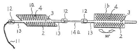
~'',~~~ar~e~aE 1
Ii.eference is jade to F'i.~. i., seeatic~I~~ ili~st~°~t~ a~
c~blit~~ae vie~r
a ~.a~nel ad~lldr~p tey~~ e~apl~ ' kph~tcoe ~:rysts.Is, ae~~r t~
Eb~ ° eat I ~f the preset veti~~. 'I'be ~~ ,eI a.ddlidr~ter eludes
a
fist 2I) ph~t~~ er3rsta~ ~a a see~~d ~I~ ph<tt~ie crystal ib. ese ~D
2~ ph~t~r~c crystals cm~t ' tr~~h-hales ~, ~~.vc~ 'les 3, aid eav~.ties 4,
e~vise as a~ the ~'i~. 5 ~:~se. t~c~~r ' fly the ~~ave ides 3 d cavvrtaes ~
c~~t ' ed ~ t3~e twc~ 2I~ pbz~t~e crystals l~ a.~d lb hive vr~ve-g~azi
° g
characteristics d rese~ara eharaeteristics that a~~: ~ detaeal ts~ eaeb ether.
CA 02459660 2004-03-04
12
1~ signal beam is introduced into th.e wa~reguide ~ in the farst ~~ photonic
crystal la frog an optical fiber 11 via, preferably, a spoi;-size converter l~
and a
microstrip wavegaide 13. °ithin light of a specific wavelength ~,1
contained in
the light incident into the ~;~aveg~aide 3 i~~ the tarst 2I~ pb.otonic crystal
la, the
light portion haviaig an electric-field vector coanponent parallel to the
principal
plane of the first 217 photo °c crystal la is trapped in its cavity 4,
from where it
is emitted.
°~he rem ' g light, which was nr~t captured in. the cavity 4 in. the
first
2I7 photonic crystal Ia, is introduced ini;o the wavrg~ide 3 an the second 2~
1Q photonic crystal 1b either directly or by means of a polarization-
gnaintaining
fiber 14a. this means that ~;lhe brat d second 2I) pbotor~c crystals 1a and lb
are connected to each other in series. in t~is case as well, it is preferable
that a
spot-size converter 1~ and a microstrip wavegaiide l~ be interpolated '
between the polarization-maintain~g fiber 14a, and the 2I~ photonic crystals
Ia d lb. at is to be str~3ssed here is that the p ' cipal planes of the first
and second 2D photonic crystals la and Ib are disposed. so as to be in a
mutually
orthogonal relationship.
~f the light of the specie wavelength ~,; within the light introduced into
the waveguide 3 in the second 2~3 photonic crystal Ib, the portion haying an
electric-held vector component orthogonal to the principal ~l a of the ~.rst
217
photonic crystal la rema3.ns_ In this situation, inasmuch as the principal
planes
of the first and sec~nd 2~ phot;onic cxystai.s la au~113 are in a mutually
orthogonal relationship, the electric-held vector component orthogonal to the
CA 02459660 2004-03-04
I3
principal plane of the first 2l7 photor~c crystal Ia is parallel to the
principal
plane of the second 21J photonic crystal lb. ~f the li;~ht of specific
wavelength ~1,
the portion having an electric-field vector coanponent parallel to the
principal
plane of the second 2~ photonic crystal Ih is thus trapped in the cavity ~ in
the
second 2D photonic crystal lb, frog where it is emitted.
'~hls means that a first light portion of specific wavelength ~,;, emitted
from the cavity ~ In the ~.r:;t 2~ photonic crystal la, and a second light
portion
of the specific wavelength ?~" emitted oau the cav:~ty 4 in the second 2D
photonic crystal Ib, have ei.ectric-field vectors that are orthogonal to each
other_
1~3 Then by detecting with photodetectors and co~pouudar~g the intensities of
these
first and second light por~~ons, tb.e proportional i~tens_~ty of the light of
the
specific ~,~avelength ~.f within the introduced sig-.nal light can be
monitored
accurately regardless of whether the light of the spea:afic wavelength ~,l is
polarized or not.
~m,bodlment 2
lieference is made to Fig. ~, schematically illustrating in an oblique view
a channel add3drop filter e.ploying 2l~ photonic crystals, accor ° g to
Eanbo ' ent 2 of the present invention. gn the chan-ael addldrop ester of
Embodiment 2 also, sixnii.arly to Eanbod~nent ~., a first ~D photonic crystal
1c
2~ d a second 2~ photor~ic ~;rystal Id are connected to ~=,ach other in series
via a
polarization-maintainia-~gfiber I~b. Waveguides and cavities contained in
these
two 2l) photonic crystals thus have wave-guiding characteristics and resonant
characteristics that are identical to each other
CA 02459660 2004-03-04
~anbodiment 2 of hig. 2, however, differs from embodiment 1 of Fig_ 1 in
that the principal planes of the first and second 2D photonic crystals lc and
ld
are disposed so as to be in a mutually parallel relata.oo.ship, and in that
the
polarization-maintaining fiber 14b is twisted about the fiber axis by a~12
from
the first 2D photonic crystal lc end to tlxe second 2~L3 plxoi;onic crystal ~
end.
In Embo ' ent 2 thus, within light of a speca~.c wavelength ~, contained
in the light incident into the waveguide ~ in the first 21~ photonic crystal
le, the
light portion ha~xxg an electric-held vector comporuent parallel to the
principal
plane of the ~.x°st 2D plaotoo.i.c crystal lc is trapped in its cavity
4, from where it
is emitted.
a rem ' g liglxt, which was not captured ix~ tlhe caty 4 in the first
2D photonic crystal lc, is introduced into the polari~at~on-maintaird.ng fiber
14b.
~f the light of the sperahc wa~eleng~h ,l within the light introduced into the
polarization-m ' t ' g iiiber lib, the portion hang <~n electric-~.e~d vector
component orthogonal to the principal plane of the f rst 2D photonic crystal
lc
remains. In this situation, inasmuch as the polarization-maim ' g fiber 14b
is twisted by n/2 from tfxe fret 2D photonic crystal lc end to the second 2D
photonic crystal ld end, i_r. turn the electric-held ~rectcar component ef the
light
portion of the specific wavelength ~1 is also rotated by ~~/2 and is
introduced. into
the waveguide in the second 213 photo~ic crystal ld.
'his means that the light portion of the specific -wavelength ~,s, which had
had the electric-~.eld vector component orthogonal witlx respect to the
principal
plane of the first 2D pbotonic cx°ystal lc, wit ' the seco»d 2D
photonic crystal
CA 02459660 2004-03-04
1d becomes parallel to its principal plane. ~'he light portion of the speci$c
wavelength ~,x having tla.~~ also °c-field vector compo_aent parallel
to the
principal plane of the second 2D photonic crystal id thus is trapped in the
cavity 4 in the second 2D photonic crystal ld, from where it is emitted.
Accordingly, a Egret light portion of specific wavelength 7~3y eanitted from
the cavity 4 in the first 2D photonic crystal lc, and a second light portion
of the
SpecC wavelength ~,1, emitted from. the cavity ~ in the second 2D photonic
crystal ld, are light portions that had had electric-field vectors in essence
orthogonal to each other. ~Jonsequently, by detecting with photodetectors and
i0 compour~di.ng the iutensi~~es c~f these first and sec.oo.d light portions,
the
proportional intensity of the Iight of the specific wavelength ~.l within the
introduced signal light cax~ be monitored accurately regardless of whether the
light of the specific wavelength ~,; is polarized or not.
~'anb~da~ent 3
lieference is made to ~'ig. 3, schematically illustrating in an oblique view
a channel addldrop filter eanploying 2D photonic crystals, according to
E~.bo ' ant 3 of the present invention. 's chaonei a.ddldrop .tar includes
first and second 2D photonic crystals le and 1f connected in parallel with
respect to a single optical fiber 11 via a 5010 optical coupler I5 and ~.rst
and
2~~ second pola~°ization-maintaining fibers 14c and 14d. These 2D
photonic crystals
contain through-holes 2, wavegaaides 3, and cavities ~, lil~ewise as ~ the
~'ig. 5
case. Actor ' gly, the waveguides and cavities cont° ' ed irr the two
~T9 photonic
crystals and have wave-guiding characteristics and resonant characteristics
CA 02459660 2004-03-04
that are identical to each o~;her.
~ optical signal ha~~ing been split ealu y b;y the r>ptical coupler 15 and
conducted into the first polarization-xnaluut ' g hbe:r ~_4c is antrod~aced
into
the waveguide 3 in the first 2D photonic cxystal le via, preferably, a spot-
size
converter 12 and a microstrip waveg-uide 13. within light of a speci$.c
wavelength ~l contained in the light incident into the waveguade 3 in the
first
2D photonic crystal ze, the light portion having an electric-held vector
coanponent parallel to the p~ncipal pl a of the fiz°st ~;D photonic
crystal le is
trapped in its cavity 4, from where it is emitted.
In a s' ' ar fashion, the ~ptical signal haviar~g keen split equ y by the
optical coupler 15 and con_ucted into the second polar~ation-xnaint ' g fiber
14d is introduced into the wavega~.de 3 i~ the second 2D photonic crystal. if
via,
preferably, a spot-size converter 1~ and a microstrip waveguide 13. 'Within
Light
of a specific wavelength ~,; contained in the light incideni; into the
waveguide 3
in the second 2D photonic crystal lf, the light portion having an electric-
field
vector component parallel to the principal plane of the second ~D photonic
crystal if is trapped in its cavity 4, from where it i:9 e~.iEted.
at is to be emphasized here° is that the principal planes of the first
and second 2D photo 'c crystals le and 11° are disposed so as to be in
a ~wutually
orthogonal relationship. °s sans that a fist light po °on of
speci.fc
wavelength ~.1, emitted from the cavity 4 in the ~.rst 2D pl~otonic crystal
le, and
a second light portion of the specific wavelength 71;, emitted from the cavity
4 in
the second 2D photonic crystal lf, have electric-field vectors that are
orthogonal
CA 02459660 2004-03-04
to each other. Accordingly, .by detecting with photodetecti'rs and con~pozan '
g
the intensities o~ these first and second light portions, the proportional
intensity of the light of the speci.~.c wavelength ~,l within the introduced
signal
light can be monitored accurately regardless o~ whether the light o~ the
specific
wavelength ~~ is polarized or not. It shoo ld be understood tbat the first and
second 21~ photonic crystals le and 1f may b~: connected. directly to the
50150
optical coupler 15, without the polarization-maintaining fibers 14c and 14d
interve ' g.
E.boe~~ent 4
1~ Reference is made to Eig. 4, schematically illustrating an an oblie~ue view
a channel addldrop filter employing 2D photonic crystals, according to
Embo ° ent 4 of the present vention. In the ~.'~annel add/drop
filter of
Embo ' ent 4 also, s° ' arly to Embodiment ~, first and second 217
photonic
crystals lg and lh are connected in parallel with respect to a single optical
fiber
i5 11 via a a0r'SQ optical coupler 3.~ dfirst and second polarization-znaant ~
ng
fibers 14e and 14.f. V~ave~~des and cavities 4 contained in these i~wo 213
photonic crystals thus nave wave-gzaiding characteristics and resonant
characteristics that are identical to each other:
Embo ' ent 4 0~ Eig. 4, however, ers fro~rn E ~'o ' ent ~ of F°ig.
3 in
20 that the principal planes othe first and second 2D~ photonic crystals lg
and lh
are disposed so as to be ~ a mutually parallel relationship, and in that the
second polar~ation-maim ' g fiber l~f is twisted. about the fiber axis by ~/2
from the optical coupler .end to the second 2photonic crystal 1h endL
CA 02459660 2004-03-04
I8
~1n optical signal havang been split equ y by the optical coupler I5 and
conducted into the first po~.ar~ation-~a ' t ' g fiber I4e is introduced into
the wave 'de 3 in the first 2D photonic crystal lg. V6~itlain light of a
specifr.c
wavelength ar contained in the light incident into the waveguide 3 in the
first
2D photonic crystal ig, the light portion having an electric-held vector
component parallel to the principal plane of the first ~a~ photonic crystal lg
is
trapped in its cavity ~, f~on~ where it is emitted_ lu the sane xn er, the
optical
signal having been split eq~.ally by the optical couplasr I;i a,nd conducted
into the
second polarization-maint ~ g fiber 14f is introd~.~ed into the wavegaide 3 in
IO the second 2D photonic crystal 1. ~T~thin light c~f a specific wavelength
~,1
contained in the light incident into the wavegaide ~ in the second ~D photonic
crystal Ih, the light portion having an ele~aric-field vector co~.p~nent
parallel to
the principal plane of the second ~D photonic crystal 1h is trapped in its
cavity 4,
from where it is emitted.
I~ What is to be emphasised herein is that the principal plaues of the first
and second ~D photonic crystals Lg and 11~ are disposed so as to be in a mut-
aally
parallel relationship, w ' ;~ the second pol atia~n-n~a:int ' g .ber l~f is
twisted about the fiber ass by ~f2 from tb.e optical a~~aupler 15 end to the
second
2D photonic crystal Ih end..
20 This means that a first light portion of spe,cifiac wavelength ,~;,
emi.tted
firo~. the cavity 4 in the brat 2D photonac crystal Ig, and a second light
portion
of the specife.c wavelength A1, emitted from the cavity 4 in the second 2D
photonic crystal Ih, are light portions that had had electric-field vectors in
CA 02459660 2004-03-04
19
essence orthogonal to each. other. accordingly, by detecting with
photodetectors
and compounding the intensities of these first and second light portions, the
proportional intensity of t:~e light of the speciC~c wavelength ~.; with:in
the
introduced signal light c be onitored accn.~'atele;~ re;~ardless of whether
the
~ light of the specific wavelength. ?~; is polarized or not. It should be
understood
that the first 2D photonic crystal lg may be connected directly to the 5015~
optical coupler 15, withcy~at t.~e first polarization-maint ~ g fiber 14e
intervening_
ruing now to the above-described embodiments considered together,
instead of the pol ation-ma~taiming fiber those embo ~ ents where it is
twisted by ~cI2 about the fber axis, a Faraday rotator or a h -wave plate can
a
utilized equivalently to rotate by a~12 the electric-held veci;or of the
light, as will
be readily apparent to those spilled in the art. In that case, the above-
described
first and second 2D photonic crystals can be fb ed s~~nciwic ' g the Faraday
rotator or the hall=wave plate, as a single-chip optical comp~nent.
In the foregoing em:bodianents, in a single ~D pbiotonic crystal. only a
single cavity is arranged. proxiynate to a single wavegai.de, but as
illustrated in
Fig. 6, by adjacently arr aging along a single wave °dLe within a
single ~D
photonic crystal a plurality of cavities 4 th at er fro one another °
resonant
frequency, a xnulti-channel add/drop filter capable of handling optical
signals in
a plurality of channels eying from each other in wavelength can be created,
as be readily apparent to th~se s ~ ed in the a~~t_
In addition, by disposing the end face of o~ptic.al fiber to co~ out each
CA 02459660 2004-03-04
2l~
cavity ~ pro ' ately, the ~a~t ~ 'tted fro the cav~~;y 4 ice. the ' action n.o
al
to tic slab 1 can be i.~trodu~:ed iota the optical fiber, d conversely, ~. be
cau
be ixa~ected into the cavity f~othe optical fiber. Fna~therre~ore, by
disposing
optoelectronic tr sducer to confront the cavity 4 ro~~nA~tely, the wavelength
of tb.e light from tl~e cavity can be o~itored, or its intensity odatio~as
received. It be rea ' y derstooby those skilled in the that a
co ' a ' ~ lens ~co ' star°a ~y be inserted ' bet~Jrer: the cavity ~ d
either
the optical-fiber end face or the o~t~electronic tr sducer.
~s liven in the fore~o~ the present ' ve:~tion ekes possible in a
~~ channel addidrop alter eplo ' 2pbotonic crystals the extraction of l~~ght
of
a specific frec~a~ea~cy at the correct relative intensity regardless of the
state of
pal ation of the i_ucident light, d ords a aveaen~°th monitor
co°bi ° ~ a
thus improved channel ~dd~drop .tar with photodeitectors.
only selected emo ' ants bane been chose~~. to illustrate the ~rese~t
~5 invention. ~'o those s ' ed irp flee t, o~rever, it v ' . a apparent f~oxn
the
fore~oi~a~ disclosure that v 'ous cb. yes d o ' .cat~.oa~.s can be ae ereirg
without depar ' ~ frog the scope of the ' vetion '~s de ein the appended
cl ° s. Faurtherore, the fog°e~oz~x~ clescrgption of thf=. eo '
ants accor ' ~ to
the present iaiventioai is provided for illustration oily, ~ d not for ' 'ting
the
20 invention as deed by tb.e f~ppended clalnxns d the=ir equivalents.