Note: Descriptions are shown in the official language in which they were submitted.
~ CA 02459838 2004-03-05
DESCRIPTION
OPTICAL RECORDING MEDIUM
TECHNICAL FIELD
The present invention relates to an optical
recording medium, and particularly to an optical recording
medium capable of recording information at high recording
density.
BACKGROUND ART
In recent years, researches and developments
concerning optical information recording systems have been
made actively in the field of information recording.
This optical information recording system has
many advantages in which it can cope with various types of
memories such as non-contact type recording and reproducing
memories, read-only memories, write-once memories and
rewritable memories, and hence a wide use from an
industrial use to a consumer use of such system has been
considered as a system that can realize inexpensive mass-
storage files.
Increase of storage capacity of optical recording
medium, for example, optical disc for use with various
kinds of information recording systems has been realized
mainly by reducing a wavelength of laser light serving as a
light source for use in an optical recording medium and by
adopting an objective lens with a high numerical aperture
(N. A.) to decrease a size of a beam spot on a focus
1
j CA 02459838 2004-03-05 1
surface .
While a CD (compact disc) affords a storage
capacity of 650 MB when it uses laser light with a
wavelength of 780 nm and an objective lens having a
numerical aperture (N. A.) of 0.45, a DVD-ROM (digital
versatile disc read-only memory) affords a storage capacity
of 4.7 GB when it uses laser light with a wavelength of 650
nm and an objective lens having a numerical aperture N. A.
of 0.6.
Further, a next-generation optical system uses an
optical disc with a thin light transmission layer having a
thickness of about 0.1 mm formed on an optical recording
layer and allows laser light to be irradiated thereon from
the side of this light transmission layer so that a large
storage capacity of greater than 22 GB can be realized by
laser light having a wavelength less than 450 nm and an
objective lens with a numerical aperture N. A. of 0.78 or
more.
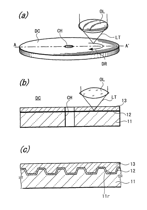
FIG. 6 (a) is a schematic perspective view
showing optical recording state or optical reproducing
state in this optical disc.
An optical disc DC is shaped like a disk with a
center hole CH bored at its center portion, and is rotated
in the direction shown by an arrow DR, for example, in FIG.
6 (a) .
FIG. 6 (b) is a schematic cross-sectional view of
2
r CA 02459838 2004-03-05 j
the optical disc. FIG. 6 (C) is an enlarged cross-
sectional view of a main portion of this optical disc DC.
This optical disc has a disc substrate 101 having
a thickness of about 1.1 mm made of polycarbonate, for
example, a concave portion lOlr formed on one major surface
of the disc substrate and an optical recording layer 102
formed along a concave and convex surface including the
concave portion lOlr.
In a phase-change type optical disc DC, for
example, its optical recording layer 102 is comprised of a
laminated layer material consisting of a dielectric film, a
phase-change film, a dielectric film and a reflective film
and the like, for example.
A light transmission layer 103 having a thickness
of 0.1 mm, for example, is formed on the optical recording
layer 102.
When information is recorded on or reproduced
from this optical disc DC, light LT of laser light having a
wavelength not more than 450 nm, for example, in a range
from 380 nm to 420 nm is focused and irradiated on the
optical recording layer 102 from the side of the light
transmission layer 103 of the optical disc DC by an
objective lens having a numerical aperture not lower than
0.78, for example, 0.85.
When recorded information is reproduced from this
optical disc, a light-receiving element receives returned
3
CA 02459838 2004-03-05
light reflected on the optical recording layer 102 and a
signal processing circuit generates a predetermined signal
to obtain a reproduced signal.
The optical recording layer 102 of this optical
disc has a concave and convex-like shape caused by the
above-mentioned concave portion lOlr formed on the surface
of the disc substrate 101.
The concave portion lOlr is formed as a
continuous groove or a circular groove shaped like a spiral,
for example, at a predetermined pitch, and the track area
is divided by the concave and convex shape.
A concave portion and a convex portion of the
concave and convex shape, which divides this track area,
are generally referred to as a "land" and a "groove". An
optical disc can increase its storage capacity with
application of a land and groove recording system for
recording information both on the land and the groove.
Moreover, only one of the land and the groove can be formed
as a recording area.
The concave and convex shape caused by the
concave portion lOlr formed on the disc substrate 101 is
formed as a pit having a length corresponding to recorded
data so that the optical disc can be formed as a read-only
memory (ROM) type optical disc.
It has been reported that tin oxide (SnOZ, z < 2)
of metal oxide having a nonstoichiometric composition can
4
CA 02459838 2004-03-05
be used as a recording material comprising an optical
recording layer (for example see Journal of Materials
Science Letters 19, 2000, 1833 to 1835).
It may be considered that this technology uses a
phenomenon in which an optical constant of a light
irradiated portion of an optical recording layer changes
due to oxidation reaction caused when the optical recording
layer is irradiated with light such as laser light.
However, when tin (Sn) is used as the recording
material, if information is recorded on the optical disc by
using an objective lens having a numerical aperture of
about 0.8 to focus short-wavelength laser light having a
wavelength ranging from about 380 nm to 420 nm on the
optical disc, then a problem arises, in which recording
marks of satisfactory shape cannot be formed so that fitter
increases.
DISCLOSURE OF THE INVENTION
A first object of the present invention is to
improve the above-mentioned fitter when Sn is used as a
recording material and a second object of the present
invention is to provide an optical recording medium capable
of stabilizing recording characteristics and improving
stability of shelf life under high temperature and high
humidity so that the optical recording medium is able to
record information satisfactorily.
An optical recording medium according to the
CA 02459838 2004-03-05
present invention comprises a substrate with a concave and
convex shape for dividing a track area formed on its
surface, at least an optical recording layer formed on a
surface in which the concave and convex shape is formed and
a light transmission layer formed on the optical recording
layer, wherein the optical recording layer is composed of a
composition SnXNYOZ (x, y, z are atomic %) of a compound of
at least tin (Sn) , nitrogen (N) and oxygen (O) , x, y, z
being selected so as to satisfy 30 < x < 70 (atomic %), 1 <
y < 20 (atomic o) and 20 < z < 60 (atomic o) .
With this arrangement, the optical recording
medium could improve fitter.
Further, an optical recording medium according to
the present invention comprises a substrate with a concave
and convex shape for dividing a track area formed on its
surface, at least an optical recording layer formed on a
surface in which the concave and convex shape is formed and
a light transmission layer formed on the optical recording
layer, wherein the optical recording layer is composed of
composition (SnxNyOZ) i-aPda (x, y, z, a are atomic %)
containing palladium (Pd) in a compound of tin (Sn),
nitrogen (N) and oxygen (0) , x, y, z, a being selected so
as to satisfy 30 < x < 70 (atomic o), 1 < y < 20 (atomic o),
20 < z < 60 (atomic %) and 1 < a < 20 (atomic %).
According to this arrangement, not only fitter
could be improved but also change of recording
6
CA 02459838 2004-03-05
characteristics could be suppressed, in particular, under
high temperature and high humidity. The reason for this
may be considered that viscosity of a recording film fused
upon recording could be increased by addition of Pd.
BRIEF DESCRIPTION OF DRAWINGS
FIG. 1 (a) is a schematic perspective view
showing the manner in which light is irradiated on an
optical disc according to an embodiment of the present
invention;
FIG. 1 (b) is a schematic cross-sectional view
taken along the line A - A' in FIG. 1 (a);
FIG. 1 (c) is a cross-sectional view showing a
main portion in an enlarged-scale;
FIGS. 2 (a) to 2 (d) are cross-sectional views
showing manufacturing processes of a manufacturing method
of an optical disc according to an embodiment;
FIG. 3 is a schematic cross-sectional view of an
optical disc according to an embodiment of the present
invention;
FIGS. 4 (a) and 4 (b) are manufacturing process
diagrams of an optical disc manufacturing method according
to an embodiment of the present invention;
FIGS. 5 (a) and 5 (b) are manufacturing process
diagrams;
FIG. 6 (a) is a schematic perspective view
showing the manner in which light is irradiated on an
7
1 .'
CA 02459838 2004-03-05
optical disc according to an example of the prior art;
FIG. 6 (b) is a schematic cross-sectional view
taken along the line A - A' in FIG. 6 (a); and
FIG. 6 (c) is a cross-sectional view showing a
main portion in an enlarged-scale.
BEST MODE FOR CARRYING OUT THE INVENTION
An optical disc of an optical recording medium
according to embodiments of the present invention will be
described below in detail. However, the present invention
is not limited to those embodiments.
[First embodiment]
FIG. 1 (a) is a schematic perspective view
showing the state in which information is recorded on or
reproduced from an optical disc DC according to this
embodiment with irradiation of light.
The optical disc DC is shaped like a disk with a
center hole CH bored thereon and is rotated in the
direction shown by an arrow DR, for example, in FIG. 1 (a).
FIG. 1 (b) is a schematic cross-sectional view of
this optical disc DC, and FIG. 1 (c) is a cross-sectional
view showing a main portion of FIG. 1(b) in an enlarged-
scale.
The optical disc DC is shaped like the disk
having the center hole CH and a concave portion llr is
formed on one major surface of a disc substrate 11 having a
thickness of about 1.1 mm made of polycarbonate, for
8
CA 02459838 2004-03-05
example. An optical recording layer 12 is formed along
concave and convex portions including this concave portion
11r, and a light transmission layer 13 is formed on this
optical recording layer 12.
The optical recording layer 12 includes a
compound of at least tin (Sn) , nitrogen (N) and oxygen (O) .
A composition SnXNYOZ of this compound is selected
so as to satisfy 30 < x < 70 (atomic %), 1 < y < 20
(atomic o) and 20 < z < 60 (atomic o) .
The optical recording layer 12 has a film
thickness ranging from 10 nm to 200 nm, for example,
approximately 30 nm to 60 nm.
The light transmission layer 13 on the optical
recording layer 12 has a thickness of 0.1 mm, for example.
The light transmission layer 13 is formed by curing a
coated film of ultraviolet-curing resin, for example.
Alternatively, the light transmission layer is constructed
by attaching a light transmission resin film made of a
suitable material such as polycarbonate with an adhesive
layer laminated thereon to the optical recording layer 12
through the adhesive layer.
When information is recorded on or reproduced
from the optical disc DC according to this embodiment, this
disc DC is rotated in the direction shown by an arrow DR
shown in FIG. 1 (a), for example, and information is
recorded on and reproduced from the optical recoding layer
9
CA 02459838 2004-03-05
12 of the optical disc DC, for example, by focusing and
irradiating laser light LT with a wavelength ranging from
380 nm to 420 nm, for example, from the side of the light
transmission layer 13 to the optical recording layer 12
through an objective lens OL having a numerical aperture of
0.85 f 0.05, for example.
When information is recorded on the optical disc,
the above-mentioned laser light LT, ,for example, is
irradiated on the optical recording layer 12 and thereby a
recording mark is formed on the light irradiated portion.
It may be considered that this recording mark is formed
when an optical constant of the light irradiated portion of
the optical recording layer 12 changes due to oxidation
reaction caused by irradiation of the above-mentioned laser
light LT.
When information is reproduced from the optical
disc, reflected light, for example, modulated by change of
the optical constant in the recording mark after laser
light has been irradiated on the optical recording layer 12
is received by a light-receiving element, it is generated
as a predetermined signal by a signal processing circuit
and is thereby outputted as a reproduced signal.
In this optical disc, the optical recording layer
12 has a concave and convex shape caused by the concave
portion llr formed on the surface of the disc substrate 11.
For example, the concave portion llr formed on
CA 02459838 2004-03-05
the disc substrate 11 is shaped like a spiral of a
predetermined pitch, that is, a spiral-like continuous
groove or, a concentric circle-like groove, and the track
area is divided by this concave and convex shape.
A pitch (distance from the center of the concave
portion to the center of the adjacent concave portion) of
this continuous groove or concentric circle-like groove,
for example, is approximately 0.32 ~ m, for example.
A convex portion and a concave portion of the
concave and convex shape that divides the track area are
generally referred to as a "land" and a "groove". Then,
the optical disc can increase its storage capacity with
application of a land and groove recording system by which
information is recorded on both of the land and the groove.
However, only one of the land and the groove can be formed
as~the recording area.
This concave and convex shape has a depth ranging
from about several manometers to 100 nm. In the case of
the groove recording system, the depth of this concave and
convex shape can be set to 20 mm. In the case of the land
and groove recording system, the depth of this concave and
convex shape can be set to 40 mm and so on.
When tin oxide (SnOZ (z < 2)) is used as a
recording material, it is to be understood from experiments
of X-ray diffraction that particles of a certain particle
11
CA 02459838 2004-03-05
size exist in the film. Since the particles contribute to
a noise component generated when the recording material is
used to form the optical disc, when a numerical aperture of
an objective lens is increased and a wavelength of laser
light is reduced in order to increase the storage capacity
of the optical disc, influence exerted by particles become
serious, and hence fitter increases.
In the optical disc according to this embodiment,
it was to be understood that a peak of X-ray diffraction
was lost by addition of at least a compound of tin,
nitrogen and oxygen, that is, nitrogen (N) as a recording
material. This indicates that the particle size of
particles in the optical recording film decreased.
Since the particle size of the particles
decreased as described above, particle influence that
causes a noise component decreases so that fitter can be
suppressed in this optical disc even when the numerical
aperture of the objective lens is increased and the
wavelength of laser light is reduced.
In the composition of the compound of tin (Sn),
nitrogen (N) and oxygen (O) used as the optical recording
layer in this optical disc, the composition ratio y of
nitrogen (N) is selected so as to satisfy 1 < y < 20
(atomic o) .
The reason for this is that if the composition
ratio of nitrogen is not more than 1 atomic %, then effect
12
CA 02459838 2004-03-05
for reducing a particle size is decreased. If it is not
less than 20 atomic o, then light absorption ratio of the
optical recording layer is lowered so that, when laser
light is irradiated on the optical recording medium, light
of intensity high enough to cause temperature to rise to
change the optical constant is required, that is,
sensitivity is lowered.
A composition ratio z of oxygen (0) in the above-
mentioned compound is selected so as to satisfy 20 < z < 60.
The reason for this is that if the composition
ratio of oxygen is not more than 20 atomic %, then oxygen
runs short and that if it is not less than 60 atomic a,
then light absorption ratio of the optical recording layer
is lowered so that, when laser light is irradiated on the
optical recording medium, light of intensity high enough to
cause temperature to rise to change the optical constant is
required, that is, sensitivity is lowered.
As described above, when the compound of nitrogen
(N) is used as the optical recording layer according to the
present invention, in the composition SnxNyOZ of the
compound of tin (Sn), nitrogen (N) and oxygen (0) is
selected so as to satisfy 30 < x < 70 (atomic %) , 1 < y <
20 (atomic o) and 20 < z < 60 (atomic %).
According to this composition, even when the
numerical aperture of the objective lens is increased and
the wavelength of the laser light is reduced, effect for
13
CA 02459838 2004-03-05
suppressing fitter can be increased.
Next, an optical disc manufacturing method
according to this embodiment will be described.
First, as shown in FIG. 2 (a), there is formed a
stamper 10 for transferring the concave and convex shape on
the disc substrate. Specifically, a convex portion lOp
that is the inverted pattern of the concave portion llr of
the disc substrate 11. shown in FIG. 1 (c) is formed on the
surface of this stamper 10.
This stamper 10 can be obtained by the following
method.
First, by a suitable method such as spin-coat, a
positive-type photoresist, for example, is coated on the
glass substrate at its smooth surface of which surface was
polished. A pattern with a shape corresponding to the
concave and convex shape of the disc substrate, such as a
desired spiral shape or concentric circle shape, is exposed
on this photoresist layer by laser light, and then this
photoresist layer is developed by alkaline developer, for
example. In this manner, there is obtained a master on
which there is formed a resist film with a pattern
corresponding to the pattern of the concave and convex
shape of the disc substrate formed by the patterned
photoresist layer.
Next, a metal layer made of a suitable material
such as nickel is deposited on this master by
14
CA 02459838 2004-03-05
nonelectrolytic plating and plating so as to have a
predetermined thickness. Thereafter, this metal layer is
released from the master. In this manner, there is formed
a stamper 10 made of the plated layer with the concave and
convex shape formed by the inverted concave and convex
shape of the above-mentioned master or there is formed the
desired stamper 10 by repeating transfer of those stampers
after a master stamper and a mother stamper have been
formed.
Next, this stamper 10 is disposed within a cavity
of a metal mold for molding the disc substrate 11, for
example, by injection molding, and molded by injection
molding of polycarbonate (PC), for example. In this
manner, as shown in FIG. 2 (b), the disc substrate 11 is
formed on the concave and convex surface of the stamper 10.
As described above, there is molded the disc
substrate 11 with the concave portion 11r, which is the
inverted concave and convex pattern, formed on the surface
by transfer of the convex portion lOp of the stamper 10.
The thus molded disc substrate 11 is released
from the stamper 10 and dusts are removed from the concave
and convex formed surface by blasting gas such as air or
nitrogen gas. Thereafter, as shown in FIG. 2 (c), a
compound layer with a predetermined composition ratio of
tin (Sn), nitrogen (N) and oxygen (O) is deposited on the
concave and convex surface by a sputtering method, for
CA 02459838 2004-03-05
example, to form the optical recording layer 12,
Next, as shown in FIG. 2 (d), the light
transmission layer 13 is formed on the optical recording
layer 12 by curing a light transmission resin material such
as ultraviolet-curing resin coated on the optical recording
layer, Alternatively, the light transmission layer is
formed by bonding a light transmission resin film made of a
suitable material such as polycarbonate .to the optical
recording layer through an adhesive layer.
In this manner, the optical disc DC having the
arrangement shown in FIG. 1 (a) could be manufactured.
When information was recorded on the inventive
optical disc DC by using an objective lens with a large
numerical aperture with irradiation of laser light having a
short wavelength, fitter could be suppressed and
information could be recorded on this optical disc
satisfactorily.
Next, a second embodiment of an optical recording
medium according to the present invention will be described.
This second embodiment has an arrangement to
remove a risk that the above-mentioned adhesive layer
comprising the light transmission layer 13 will be
denatured when temperature of the recording layer is raised
and the recording layer is heated with irradiation of laser
light to record information, that is, to form recording
marks on the optical recording medium.
16
CA 02459838 2004-03-05
[Second embodiment]
FIG. 3 is a schematic cross-sectional view of an
optical disc according to this embodiment.
An optical disc according to this embodiment is
substantially similar to the above-mentioned optical disc
according to the first embodiment and has an arrangement in
which a protective film 14 for protecting the optical
recording layer 12 is interposed between the optical
recording layer and the light transmission layer l3.
Also in this embodiment, the concave portion llr
is formed on one major surface of the disc substrate 11
made of polycarbonate, for example, having a thickness of
approximately 1.1 mm, for example. Also, the optical
recording layer 12 is formed on the concave and convex
surface including the concave portion 11r.
Also in this embodiment, similarly to the first
embodiment, the optical recording layer 12 has a compound
of at least tin (Sn), nitrogen (N) and oxygen (O). This
compound composition SnXNyOZ of the compositions of tin (Sn),
nitrogen (N) and oxygen (0) should preferably be selected
so as to satisfy 30 < x < 70 (atomic %), 1 < y < 20
(atomic %) and 20 < z < 60 (atomic o) .
This optical recording layer 12 has a thickness
ranging from 10 nm to 200 nm, in this case, in a range from
approximately 50 nm to 60 nm, for example.
In this embodiment, this optical recording layer
17
CA 02459838 2004-03-05
12 has deposited thereon the protective film 14 made of a
light transmission dielectric film such as silicon oxide,
for example.
This protective film 14 has a thickness ranging
from 5 nm to 100 nm, for example, 30 nm.
The light transmission layer 13 having a
thickness of 0.1 mm, for example, is deposited on this
protective film 14. This light transmission layer 13 is
constructed in such a manner that a light transmission
resin film made of a suitable material such as
polycarbonate with an adhesive layer, for example,
laminated thereon is bonded to the protective film 14 by
the adhesive layer.
According to the arrangement for interposing the
protective film 14 between the optical recording layer and
the light transmission layer as seen in this embodiment,
even when the optical disc is brought to the high
temperature state with irradiation of laser light to form
recording marks, since the protective film 14 is interposed
between the optical recording layer and the light
transmission layer, the adhesive layer in the light
transmission layer 13 can be prevented from being denatured
to thereby protect the optical recording layer 12 from
being affected.
Next, an optical disc manufacturing method
according to the second embodiment will be described.
18
CA 02459838 2004-03-05
First, as shown in FIG. 4 (a) , according to the
procedure described in the first embodiment, there is
formed the disc substrate 11 with the concave and convex
shape including the concave portion llr for dividing the
track area formed on the surface thereof.
Next, after dusts have been removed from this
disc substrate 11 on its concave and convex shape formed
surface by blasting gas such as air and nitrogen gas onto
the above surface, the optical recording layer 12 of the
above-mentioned composition consisting of the compound of
tin, nitrogen and oxygen is formed by a suitable method
such as a sputtering method as shown in FIG. 4 (b).
Next, as shown in FIG. 5 (a), silicon oxide is
deposited by a suitable method such as a sputtering method
to thereby form the protective film 14.
Thereafter, as shown in FIG. 5 (b), the light
transmission layer 13 is formed by bonding the light
transmission resin film made of a suitable material such as
polycarbonate onto the protective film 14 with the adhesive
layer.
In this manner, the optical disc having the
arrangement shown in FIG. 3, that is, optical recording
medium can be manufactured.
According to the optical disc of this second
embodiment, similarly to the first embodiment, even when
information is recorded on the optical disc using tin as
19
CA 02459838 2004-03-05
the recording material with irradiation of laser light
having a short wavelength from an objective lens having a
large numerical aperture, fitter can be suppressed, and
hence information can be recorded on the optical disc
satisfactorily.
The above-mentioned optical disc according to the
present invention, that is, optical recording medium will
be described with reference to specific inventive examples
and comparative examples which are in contrast with the
present invention.
(Inventive example 1)
There was formed a disc substrate with a concave
and convex shape to divide a track area formed on its
surface. The concave and convex shape was a continuous
groove formed like spirals at a pitch of 0.32 ~.sm, and the
concave and convex shape had a depth of 20 nm. A
composition of SnXNyOZ (x = 31 atomic %, y = 10 atomic o, z
- 59 atomic %) having a thickness of 50 nm was deposited on
the disc substrate at its concave and convex shape formed
surface by sputtering so as to satisfy this composition
ratio to thereby form an optical recording layer. Further,
a protective film was formed by depositing silicon oxide
having a thickness of 30 nm on the optical recording layer,
and a light transmission layer having a thickness of 0.1 mm
was formed by bonding a light transmission resin film made
CA 02459838 2004-03-05
of a suitable material such as polycarbonate onto the
protective film with an adhesive layer. In this manner,
an optical disc sample A was manufactured.
A random signal with a bit length of 0.13 ,um was
recorded on this sample A with irradiation of recording and
reproducing laser light having a wavelength of 405 nm from
an objective lens having a numerical aperture of '0.85 by a
test system having an optical system for focusing light on
the optical recording layer of the optical disc.
The signal that has been recorded on the optical
disc had fitter of 90.
(Comparative example 1)
This comparative example had a similar
arrangement to that of the inventive example 1 but the
composition of the optical recording layer was changed to
SnXNyOz (x = 30 atomic o, y = 10 atomic o, z = 60 atomic %)
and an optical disc sample B was manufactured.
A random signal having a bit length of 0.13 ,um
was recorded on this sample B by the test system described
in the inventive example 1. Jitter at that time was 15%.
In general, if fitter exceeds 13%, then it is
difficult to reproduce information from the optical disc at
high accuracy. Therefore, the optical recording medium,
for example, optical disc has requirements in which fitter
should be not more than 130.
21
CA 02459838 2004-03-05
(Comparative example 2)
This comparative example had a similar
arrangement to that of the inventive example 1 but the
composition of the optical recording layer was changed to
SnxNyOZ (x = 25 atomic %, y = 10 atomic %, z = 65 atomic o)
and an optical disc sample C was manufactured.
Although a random signal having a bit length of
0 . 13 a m was recorded on this sample C by the test system
shown in the inventive example l, a signal was not recorded
on this sample, and hence fitter could not be measured.
(Inventive example 2)
This inventive example had a similar arrangement
to that of the inventive example 1 but the composition of
the optical recording layer was changed to SnXNyOZ (x - 69
atomic o, y = 10 atomic %, z = 21 atomic o) and an optical
disc sample D was manufactured.
A random signal having a bit length of 0.13 ~ m
was recorded on this sample D by the test system described
in the inventive example 1. Jitter at that time was 100.
(Comparative example 3)
This comparative example had a similar
arrangement to that of the inventive example 1 but the
composition of the optical recording layer was changed to
SnXNyOZ (x = 70 atomic o, y = 10 atomic %, z = 20 atomic %)
and an optical disc sample E was manufactured.
22
CA 02459838 2004-03-05
A random signal having a bit length of 0.13' a m
was recorded on this sample E by the test system described
in the inventive example 1. Jitter at that time was 16%.
This fitter exceeds 130, and hence it was to be understood
that this comparative example is not suitable for the
application to the optical disc.
(Comparative example 4)
This comparative example had a similar
arrangement to that of the inventive example 1 but the
composition of the optical recording layer was changed to
SnXNyOZ (x = 75 atomic %, y = 10 atomic %, z = 15 atomic %)
and an optical disc sample F was manufactured.
Although a random signal having a bit length of
0 . 13 !~ m was recorded on this sample F by the test system
described in the inventive example l, no signal was
recorded on this disc sample and hence fitter could not be
measured.
(Inventive example 3)
This inventive example had a similar arrangement
to that of the inventive example 1 but the composition of
the optical recording layer was changed to SnXNyOZ (x - 45
atomic %, y = 2 atomic %, z - 53 atomic o) and an optical
disc sample G was manufactured.
A random signal having a bit length of 0.13 a m
was recorded on this sample G by the test system described
23
CA 02459838 2004-03-05
in the inventive example 1. fitter at that time was 10%.
(Comparative example 5)
This comparative example had a similar
arrangement to that of the inventive example 1 but the
composition of the optical recording layer was changed to
SnXNyOZ (x - 45 atomic %, y = 1 atomic o, z - 54 atomic %)
and an optical disc sample H was manufactured.
A random signal having a bit length of 0.13 a m
was recorded on this sample H by the test system described
in the inventive example 1. fitter at that time was 14%.
This fitter exceeds 13%, and hence it was to be understood
that this comparative example is not suitable for the
application to the optical disc.
(Inventive example 4)
This inventive example had a similar arrangement
to that of the inventive example 1 but the composition of
the optical recording layer was changed to SnXNyOz (x - 45
atomic o, y = 19 atomic %, z - 36 atomic o) and an optical
disc sample I was manufactured.
A random signal having a bit length of 0.13 ,um
was recorded on this sample I by the test system described
in the inventive example 1. fitter at that time was 100.
(Comparative example 6)
This comparative example had a similar
arrangement to that of the inventive example 1 but the
24
CA 02459838 2004-03-05
composition of the optical recording layer was changed to
SnXNyOZ (x = 45 atomic o, y = 20 atomic o, z = 35 atomic %)
and an optical disc sample J was manufactured.
A random signal having a bit length of 0.13 I~m
was recorded on this sample J by the test system described
in the inventive example 1. Jitter obtained at that time
was 14%, which was an unsatisfactory result.
A study of measured results of jitters of the
samples of the inventive examples and the comparative
examples reveals that the optical recording medium having
the inventive optical recording layer composed of the
compound of tin (Sn), nitrogen (N) and oxygen (O), its
composition SnXNyOZ being selected so as to satisfy 30 < x <
70 (atomic %) , 1 < y < 20 (atomic %) , 20 < z < 60
(atomic %) can improve fitter.
Specifically, although the above-mentioned first
and second embodiments can improve fitter, when the optical
recording layer is composed of tin oxide and tin nitride
SnXNyOZ as in the above-mentioned embodiments, viscosity of
the optical recording layer is relatively low in the state
in which the optical recording layer is fused with
irradiation of laser light. As a result, improvement of
fitter is restricted or improvement of shelf life under
high temperature and high humidity is restricted.
On the other hand, according to the present
CA 02459838 2004-03-05
invention, there is provided an optical recording medium
having high resistance against high temperature and high
humidity and in which sharpness of recording marks can
increase to improve fitter and stability of shelf life.
In the optical recording medium having this
arrangement according to the present invention, its
recording layer has an arrangement in which palladium Pd,
which is a high melting point metal, of 1 atomic o to 20
atomic a is mixed into a compound of SnXNyOZ selected so as
to satisfy 30 < x < 70 (atomic o) , 1 < y < 20 (atomic %) ,
20 < z < 60 (atomic %) .
Specifically, with this arrangement, when
information is recorded on this optical recording medium
with irradiation of laser light, viscosity obtained when
the recording layer is fused can increase to improve
lowered sharpness and fluctuation of position of recording
marks, which can improve fitter and shelf life much more.
An embodiment of the optical recording medium
having this arrangement will be described.
[Third embodiment]
Also in this embodiment, similarly to the first
embodiment, the optical disc DC is shaped like the disc
with the center hole CH bored thereon as FIG. 1 (a) shows a
schematic perspective view. The disc substrate 11 having
a thickness of approximately 1.1 mm made of polycarbonate,
for example, has the concave portion llr formed on its one
26
CA 02459838 2004-03-05
major surface. As shown in FIGS. 1 (b) and 1 (c), the
optical recording layer 12 is formed along concavities and
convexities including this concave portion 11r, and the
light transmission layer 13 is formed on this optical
recording layer 12.
The optical recording layer 12 has a mixture in
which palladium Pd was mixed to a compound of at least tin
(Sn) , nitrogen (N) , oxygen (O) (SnXNYOZ are selected so as
to satisfy 30 < x < 70 (atomic o) , 1 < y < 20 (atomic %) ,
20 < z < 60 (atomic %)). Palladium Pd has a concentration
which falls within a range from 1 atomic o to 20 atomic %.
Similarly to the first embodiment, the optical
recording layer 12 has a film thickness ranging from 10 nm
to 200 nm, for example, 30 nm to 60 nm.
The light transmission layer 13 having a
thickness of 0.1 mm, for example, is formed on the optical
recording layer 12. This light transmission layer 13 is
formed by curing a coated film of an ultraviolet-curing
resin. Alternatively, the light transmission layer is
formed by bonding a light transmission resin film made of a
suitable material such as polycarbonate with an adhesive
layer laminated thereon to the optical recording layer 12
through the adhesive layer.
When information is recorded on or reproduced
from the optical disc DC according to this embodiment, this
disc DC is rotated in the direction shown by the arrow DR
27
CA 02459838 2004-03-05
in FIG. 1 (a) and the optical recording layer 12 of the
optical disc DC, for example, is irradiated with laser
light LT having a wavelength ranging from 380 nm to 420 nm,
for example, and focused on the optical recording layer 12
from the side of the light transmission layer 13 through an
objective lens OL having a numerical aperture of 0.85 t
0.05, for example.
When information is recorded on the optical disc,
the above-mentioned laser light LT irradiates the optical
recording layer 12 to form recording marks on the portion
irradiated with the laser light. As mentioned before,
this recording mark is formed when an optical constant of
the light irradiated portion of the optical recording layer
12 is changed due to oxidation reaction caused by
irradiation of the above-mentioned laser light LT.
When information is reproduced from the optical
disc, reflected light, for example, modulated by change of
the optical constant in the recording mark after laser
light has been irradiated on the optical recording layer 12
is received by a light-receiving element, it is generated
as a predetermined signal by a signal processing circuit
and is thereby outputted as a reproduced signal.
In this optical disc, the optical recording layer
12 has concave and convex shapes caused by the concave
portion llr formed on the surface of the disc substrate 11.
For example, the concave portion llr formed on
28
CA 02459838 2004-03-05
the disc substrate is shaped .like a spiral of a
predetermined pitch, a spiral-like continuous groove or a
concentric circle-like groove, and the track area is
divided by this concave and convex shape.
A pitch (distance from the center of the concave
portion to the center of the adjacent concave portion) of
this continuous groove or concentric circle-like groove,
for example, is approximately 0.32 a m, for example.
A convex portion and a concave portion of the
concave and convex shape that divides the track area are
generally referred to as a "land" and a "groove". Then,
the optical disc can increase its storage capacity with
application of a land and groove recording system by which
information is recorded on both of the land and the groove.
However, only one of the land and the groove can be formed
as the recording area.
The depth of this concave and convex shape falls
within a range from approximately several nanometers to 100
nm. In the case of the groove recording system, for
example, the depth of the concave and convex shape can be
set to 20 nm. In the case of the land and groove recording
system, the depth of the concave and convex shape can be
set to 40 nm.
Since the optical disc according to this
embodiment uses the recording material consisting of the
29
CA 02459838 2004-03-05
mixture in which Pd is mixed into the compound of at least
tin, nitrogen and oxygen, viscosity obtained when the
recording layer is fused can be increased and the
fluctuations of the position of the recording mark and the
shape of the recording mark can be suppressed, thereby
increasing the recording density. Specifically, since the
optical disc can increase its storage capacity, even when
the numerical aperture of the objective lens is increased
and the wavelength of the irradiated laser light is reduced,
fitter can be suppressed. Also, recording characteristics
under high temperature and high humidity can be improved,
and shelf life can be stabilized.
The concentration of Pd added to the compound of
tin (Sn), nitrogen (N), oxygen (0) comprising the optical
recording layer in the optical disc according to this
embodiment is selected in a range from 1 atomic % to 20
atomic o. If this concentration is less than 1 atomic %,
then fluidity suppressing effect decreases and the above
improvement of the shelf life stability becomes
insufficient. If this concentration exceeds 20 atomic %,
then melting point and thermal conductivity increase too
much, and hence recording sensitivity is lowered.
Therefore, the concentration of Pd is selected in
a range from 1 atomic % to 20 atomic %.
An optical disc manufacturing method according to
this embodiment will be described.
. CA 02459838 2004-03-05
Also in this case,the stamper 10 is formed by a
similar method to that has been described with reference to
FIG. 2 (a). Specifically, a convex portion lOp of the
inverted pattern of the concave portion llr of the disc
substrate 11 shown in FIG. 1 (c) is formed on this stamper
10.
Next, this stamper 10 is disposed within the
cavity of the.metai mold used to mold the disc substrate 11,
for example, by injection molding and thereby molded by
injection molding of polycarbonate (PC). In this manner,
the disc substrate 11 is formed on the concave and convex
surface of the stamper 10 as shown in FIG. 2 (b).
In this manner, there is formed the disc
substrate 11 in which the concave portion llr which is the
concave and convex shape of the inverted pattern is formed
by transferring the pattern of the convex portion lOp of
the stamper 10 to the surface.
The thus molded disc substrate 11 is released
from the stamper 10 and dusts are removed from the concave
and convex formed surface by blasting gas such as air and
nitrogen gas to the concave and convex formed surface.
Thereafter, as shown in FIG. 2 (c), the optical recording
layer 12 is formed by depositing the material layer in
which Pd of a predetermined added amount is mixed into the
compound of a predetermined composition ratio of tin (Sn),
nitrogen (N) and oxygen (O) according to the sputtering
3~
CA 02459838 2004-03-05
s
method, for example.
Next, as shown in FIG. 2 (d), by a procedure and
a method similar to those that have been described in the
manufacturing method according to the aforementioned first
embodiment, the light transmission layer 13 is formed on
the optical recording layer 12.
In this way, the optical disc DC having the
arrangement shown in FIG. 1 (a) can be manufactured.
Next, a fourth embodiment will be described.
According to the fourth embodiment, the optical
recording medium of the above-mentioned third embodiment
may have an arrangement to prevent the above-mentioned
adhesive layer comprising the light transmission layer 13
from being denatured due to rise of temperature of the
recording layer heated with irradiation of laser light when
information is recorded, that is, recording mark is formed.
[Fourth embodiment]
An optical disc according to this embodiment has
a schematic cross-section similar to that described in FIG.
3.
Although the optical disc according to this
embodiment is substantially similar to the above-mentioned
optical disc according to the third embodiment, the
protective film 14 for protecting the optical recording
layer 12 is interposed between the optical recording layer
12 and the light transmission layer 13.
32
CA 02459838 2004-03-05
Also in this case, the concave portion llr is
formed on one major surface of the disc substrate 11 having
a thickness of about 1.1 mm, for example, made of
polycarbonate, for example. The optical recording layer
12 is formed along the concave and convex surface including
the concave portion 11r.
Also in this embodiment, similarly to the third
embodiment, the optical recording layer 12 has the
arrangement in which Pd of 1 to 20 atomic % is mixed into
the compound of SnXNyOZ of which composition ratio satisfies
30 < x < 70 (atomic %), 1 < y < 20 (atomic o), 20 < z < 60
(atomic %) .
This optical recording layer 12 has a thickness
ranging from 10 nm to 200 nm, in this case, in a range from
approximately 30 nm to 60 nm.
Then, also in this embodiment, the protective
layer 14 made the light transmission dielectric film made
of a suitable material such as silicon oxide is formed on
this optical recording layer 12.
The film thickness of this protective film 14 is
selected in a range from 5 nm to 100 nm, for example, 30 nm.
The light transmission layer 13 having a
thickness of 0.1 mm, for example, is formed on this
protective film 14. This light transmission layer 13 is
constructed by bonding the light transmission resin film
made of a suitable material such as polycarbonate with an
33
CA 02459838 2004-03-05
adhesive layer, for example, laminated thereon to the
protective film 14 through the adhesive layer.
According to the arrangement in which the
protective film 14 is formed on the optical recording layer
as seen in this embodiment, even when the optical recording
layer is heated at high temperature with irradiation of
light to form the recording marks, the existence of the
protective film 14 can suppress the recording and
reproducing characteristics from being deteriorated due to
the increase of noise caused by the denatured light
transmission layer 13.
Next, an optical disc manufacturing method
according to this embodiment will be described.
First, as shown in FIG. 4 (a), according to the
procedure described in the first embodiment, there is
formed the disc substrate 11 with the concave and convex
shape including the concave portion llr for dividing the
track area formed on the surface thereof.
Next, after dusts have been removed from this
disc substrate 11 on its concave and convex shape formed
surface by blasting gas such as air and nitrogen gas onto
the above surface, the optical recording layer 12 of the
mixture of Pd mixed into the above-mentioned composition
consisting of the compound of tin, nitrogen and oxygen is
formed by a suitable method such as a sputtering method as
shown in FIG. 4 (b).
34
CA 02459838 2004-03-05
,""
Next, as shown in FIG. 5 (a), silicon oxide is
deposited by a suitable method such as a sputtering method
to thereby form the protective film 14.
Thereafter, as shown in FIG. 5 (b), the light
transmission layer 13 is formed by bonding the light
transmission resin film made of a suitable material such as
polycarbonate onto the protective film 14 with the adhesive
layer.
In this manner, the optical disc having the
arrangement shown in FIG. 3, that is, optical recording
medium can be manufactured.
The above-mentioned optical recording medium
formed of the optical recording layer with Pd mixed thereto
according to the present invention will be described with
reference to specific inventive examples.
(Inventive example 5)
There was formed a disc substrate With a concave
and convex shape to divide a track area formed on its
surface. The concave and convex shape was a continuous
groove formed like a spiral at a pitch of 0.32 a m, and the
concave and convex shape had a depth of 20 nm. A
composition of (SnXNYOZ) i-aPda (x - 31 atomic %, y - 10
atomic o, z - 59 atomic %, a - 1 atomic o) having a
thickness of 50 nm was deposited on the disc substrate at
its concave and convex shape formed surface by sputtering
CA 02459838 2004-03-05
so as to satisfy this composition ratio to thereby form an
optical recording layer. Further, a protective film was
formed by depositing silicon oxide having a thickness of 30
nm on the optical recording layer, and a light transmission
layer having a thickness of 0.1 mm was formed by bonding a
light transmission resin film made of a suitable material
such as polycarbonate onto the protective film with an
adhesive layer. In this manner, an optical disc sample K
was manufactured.
A random signal with a bit length of 0.13 a m was
recorded on this sample K with irradiation of recording and
reproducing laser light having a wavelength of 405 nm from
an objective lens having a numerical aperture of 0.85 by a
test system having an optical system for focusing light on
the optical recording layer of the optical disc.
Jitter of the signal that has been recorded on
the optical disc was 8%.
A change of transmittance obtained after the
sample K has been kept at temperature of 80°C with relative
humidity of 85% for 100 hours was less than 1%.
(Comparative example 7)
This comparative example had a similar
arrangement to that of the inventive example 5 but the
composition of the optical recording layer was changed to
(SnXNyOZ) i-aPda (x - 31 atomic %, y - 10 atomic %, z - 59
36
, CA 02459838 2004-03-05
,,
atomic %, a - 0.9 atomic o) and an optical disc sample L
was manufactured.
A random signal having a bit length of 0.13 lam
was recorded on this sample L by the test system described
in the inventive example 5. fitter obtained at that time
was 10%.
(Inventive example 6)
This inventive example had a similar arrangement
to that of the inventive example 5 but the composition of
the optical recording layer was changed to (SnXNyOZ) i-aPda (x
- 31 atomic o, y - 10 atomic o, z - 59 atomic o, a - 20
atomic %) and an optical disc sample M was manufactured.
A random signal having a bit length of 0.13 a m
was recorded on this sample M by the test system described
in the inventive example 5. fitter obtained at that time
was 9 0 .
A change of transmittance obtained after the
sample M has been kept at temperature of 80°C with relative
humidity of 85% for 100 hours was less than lo.
(Comparative example 8)
This comparative example had a similar
arrangement to that of the inventive example 5 but the
composition of the optical recording layer was changed to
(SnXNyOZ) i-aPda (x - 31 atomic o, y - 10 atomic o, z - 59
atomic %, a = 21 atomic ~) and an optical disc sample N was
37
CA 02459838 2004-03-05
manufactured.
A random signal having a bit length of 0.13 ~cm
was recorded on this sample N by the test system described
in the inventive example 5. Jitter obtained at that time
was 16%.
As is clear from the measured results of jitters
of the above-mentioned samples K, M of the present
invention and the samples L, N of the comparative examples,
it is to be understood that the optical recording medium in
which the optical recording layer according to the present
invention is composed of the compound of tin (Sn), nitrogen
(N) and oxygen (O) with Pd mixed thereto can improve fitter
and resistance against high temperature and high humidity.
It is needless to say that the optical recording
medium according to the present invention is not limited to
the above-mentioned embodiments and inventive examples and
that the arrangement of the present invention can be
modified and changed in various points such as shapes of
optical memory card, optical memory sheet and structures of
layers of laminating layer.
As described above, according to the optical
recording medium of the present invention, since the
compound composition comprising the optical recording layer
is selected to be SnXNyOZ and 30 < x < 70 (atomic %) , 1 < y
< 20 (atomic o) and 20 < z < 60 (atomic %) are satisfied,
38
CA 02459838 2004-03-05
the problems of fitter caused when information is recorded
on the recording medium using tin as the recording medium
as mentioned in the preamble is irradiated with laser light
having a short wavelength by an objective lens with a large
numerical aperture can be solved.
Further, in the optical recording medium
according to the present invention, since Pd is mixed into
the compound SnXNYOZ comprising the optical recording layer,
viscosity obtained when the recording layer is fused with
irradiation of laser light can be increased and
fluctuations of position and shape of the recording mark
can be suppressed, the optical recording medium can
increase recording density. Specifically, even when the
numerical aperture of the objective lens is increased and
the wavelength of the irradiated laser light is reduced in
order to increase the storage capacity, the fitter can be
suppressed. Moreover, the recording characteristic
obtained under high temperature and high humidity can be
improved, and hence the optical recording medium having
more excellent recording characteristic can be constructed.
As described above, according to the arrangement
of the present invention, there can be achieved a large
effect in which a large-storage optical recording medium
with excellent recording characteristics can be obtained.
39