Note: Descriptions are shown in the official language in which they were submitted.
CA 02459975 2004-03-08
WIIZ'EI/ESS C h/MUNlCA'Tlt3N CIRCUIT
Background of the 'Inverition
The invention relates generally to analysis of geologic formations in
furtherance of
exploitation of hydrocarbon reservoirs present therein. More particularly, the
present
invention is directed to a wireless communication circuit suited for use in
analysis of geologic
forrnations.
Geologic formations defining a reservoir for the accumulation of hydrocarbons
in the
sub-surface of the earth contain a network of interconnected paths iri vrhich
fluids are
disposed that ingress or egress fronn the reservoir. ~ o determine the nature
and behavior of
the fluids in the aforementioned network, knowledge of the geologic formation
is desired,
such as, reservoir pressure and the permeability of tiie reservoir rock.
11'resent day operations
analyze these characteristics either i;hrough wireline logging via a"formation
tester" tool or
tJhrough drill stem tests. Both types of tests are suitable for use with "open-
hole" or "cased-
hole" applications. However, these tests do not afford real-time data
acquisition, because it is
required to perform the tests once the drilling equipment has beera removed
from the hole,
referred to as a trip.
A trip typically involves renioving the drill string from the wel l bore,
running a
forrnation tester into the well bore to acquire the format.ion data, and,
after retrieving the
forrnation tester, running the drill string back into ffie well bore tbr
further drilling. As is
evident "tripping the well" reduces throughput and, as such, is typically
avoided. As a result,
data acquisition usually occurs vvhe;a it is convenient, e.g., during a drill
bit change, or vvhen
the drill string is being removed for some other drilling unrelated reason, or
when data
acquisition is sufficiently important to J'ustify a supplemental trip.
Obtaining reservoir formation data on a "real time" basis is desired and
beneficial. As
a result, there has been prior art attempts to acquire various fom aation data
from a sub-si.irface
1
CA 02459975 2009-03-12
'79350-108
zone of interest while the drill string is present within the well bore. One
prior art attempt is
disclosed by Ciglenec et al. in U.S. Pat. No. 6,028,534, which is assigned to
the assignee of
the present invention. Ciglenec et al. disclose a remote sensor containing
sensor
instrumentation and associated electronics that is ballistically deployed into
a formation. The
electronics contained in the remote sensor facilitate data transfers between
the sensor and an
adjacent collar that is rotating. To that end, the electronics allow
determining the desired
spatial orientation between the collar and the sensor before data
communication occurs.
A need exists, therefore, to provide electronics suitable for use in wireless
communication circuits deployed in geologic formations.
SUMMARY OF THE INVENTION
Embodiments of the invention include a communication circuit and a method of
communicating
with wireless signals that features providing a tank circuit having ari
inductor connected in parallel
with a capacitor circuit. The inductor is the antenna of the communication
circuit and,
therefore, always operates in resonance, even when the tank circuit components
change with
temperature. The antenna can, therefore, operate at a high Q with minimal
power
consumption when transmitting. The capacitor circuit includes a pair of
capacitors coupled in
series. Each of the capacitors is connected in common to ground and has a
capacitive value
associated. A feedback network is connected to selectively bias the tank
circuit to produce a
signal, while minimizing the power required to produce the signal. The
feedback circuit
operates to maximize the amplitude swing of the signal produced across the
antenna. The
single ended amplitude of the signal on each side of the antenna is a function
of a ratio of the
capacitive values associated with the capacitor circuit, with the frequency of
the signal being
defined by the inductor and the capacitor circuit. The tank circuit is
multifunctional in that it
may be biased to function as a transmitter and/or a receiver. Additionally,
the tank circuit
may be augmented with additional circuits that more clearly define the
transmission or
2
CA 02459975 2009-03-12
79350-108
reception frequency, as well as to provide a remote power
source for the same. These and other embodiments are
discussed more fully below.
One aspect of the invention provides a wireless
communication circuit, comprising; an antenna; a capacitor
circuit connected in parallel with said antenna, defining a
tank circuit having first and second ports, with said
capacitor circuit including a pair of capacitors coupled in
series, said pair of capacitors being connected in common to
ground; and a feedback network connected to said tank
circuit to selectively bias said tank circuit to operate as
a transmitter and a receiver.
There is also provided a communication circuit,
comprising: a tank circuit having an inductor connected in
parallel with a capacitor circuit, said capacitor circuit
including a pair of capacitors connected in series, with
said pair of capacitors having first and second values
associated therewith and being connected in common to
ground; and a feedback network connected to said tank
circuit to selectively bias said tank circuit to operate as
a transmitter and a receiver.
Another aspect of the invention provides a method
of communicating with wireless signals with a tank circuit
connected to a feedback network, said method comprising:
forming said tank circuit by connecting an antenna in
parallel with a capacitor circuit so that said antenna
continuously operates in resonance; and producing an
oscillatory signal by selectively biasing said tank circuit
with said feedback network to operate said tank circuit as a
transmitter and a receiver.
3
CA 02459975 2009-03-12
79350-108
BRIEF DESCRIPTION OF THE DRAWINGS
Fig. 1 is a diagram of a drill collar positioned in a borehole and equipped
with a
steerable transceiver unit in accordance with an embodiment of the present
invention;
Fig. 2 is a schematic illustration of the steerable transceiver unit of the
drill collar of
Fig. 1 showing a system for emplacing a remote sensor from the borehole into a
selected sub-
surface formation;
Fig. 3 schematically diagrams the electronic circuitry of the steerable
transceiver unit
of the drill collar of Fig. I for receiving data signals from and transmitting
signals to the
remote sensor;
Fig. 4 is an electronic block diagram schematically illustrating the
electronics of a
remote sensor;
Fig. 5 is a schematic illustration of a communication circuit shown in Fig. 4
in
accordance with a first embodiment;
Fig. 6 is a schematic illustration of a communication circuit shown in Fig. 4
in
accordance with a second embodiment;
Fig. 7 is a schematic illustration of a communication circuit shown in Fig. 4
in
accordance with a third embodiment;
Fig. 8 is a schematic illustration of a communication circuit shown in Fig. 4
in
accordance with a fourth embodiment;
Fig. 9 is a schematic illustration of a communication circuit shown in Fig. 4
in
accordance with a fifth embodiment;
Fig. 10 is a schematic illustration of a communication circuit shown in Fig. 4
in
accordance with a sixth embodiment; and
3a
CA 02459975 2009-03-12
79350-108
Fig. 11 is a block diagram conceptually illustrating operation of the
steerable
transceiver unit in conjunction with the remote sensor in accordance with an
embodiment of the
present invention.
DETAILED DESCRIPTION OF THE INVENTION
Referring to Fig. 1, an exemplary use of the present invention involves a
drill collar
that includes a drill string (not shown) for drilling a well bore 12. Drill
collar 10 is
provided with a sonde section 14 including a data acquisition circuit 16,
shown in Fig. 2,
incorporating transmitter/receiver circuitry 18 of Fig. 3.
Referring to Fig. 2, drill collar 10 includes a pressure gauge 20 whose
pressure sensor
22 is exposed to borehole pressure in well bore 12 via a drill collar passage
24. Pressure
gauge 20 senses ambient pressure at the depth of a selected sub-surface
formation and is used
to verify pressure calibration of remote sensors. Electronic signals (not
shown) representing
ambient well bore pressure are transmitted via pressure gauge 20 to the
circuitry of data
acquisition circuit 16. Data acquisition circuit 16 then performs a pressure
calibration of a
remote sensor 26, shown best in Fig. 1, being deployed at that particular well
bore depth.
Drill collar 10 is also provided with one or more remote sensor receptacles
28, also
shown in Fig. 1. Each sensor receptacle 28 contains a remote sensor 26 for
positioning
within a selected sub-surface formation of interest intersected by well bore
12. As will be
discussed further below, remote sensor 26 is positioned, in this particular
embodiment, while
well bore 12 is being drilled. Note, however, that remote sensor 26 may be
previously
emplaced and used in conjunction with the steerable transceiver unit of the
present invention.
In such embodiments, efforts will typically need to be made to identify the
location of remote
sensor 26, as is discussed more fully below.
Remote sensors 26 are encapsulated "intelligent" sensors that are moved from
drill
collar 10 to a position within the formation surrounding well bore 12. Remote
sensors 26
4
CA 02459975 2004-03-08
sense formation characteristics such as pressure, temperature, rock
permeability, porosity,
conductivity, and dielectric constant, among others. Remote sensors 26 are
appropriately
encapsulated in a sensor housing of sufficient structural integrity to
withstand damage during
movement from drill collar 10 into laterally embedded relatioii .vitt'i tlae
sub-su.rface
.
formation surrounding well bore 12
Referring again to Fig. 1, a single remote sensor 26 is shown embedded in a
formation
in a roughly perpendicular orientation relative to well bore 12 and, hence,
drill collar 10.
'I'hose skilled in the art having the benefit of this d::_selosure will
appreciate that such lateral
embedding movement need not be perpendicular to well bore 1.2, but may be
accomplished
through numerous angles of attack into the desired fonnation positIon_ Sensor
deployment
can be achieved utilizing one or nlore of the following: (1) drilling into
borehole wa1130 and
placing remote sensor 26 into the forrnation9 (2) pr,~:nching/pressing thc
encapsulated rernote
sensors 26 into the formation. with a hydraulic press or other mechanical
penetration
assembly; or (3) shooting remote &-,nsors 26 into the formation by utilizing
propellant
charges. Any of these techniques are suitable, depending on the
irr:iplementation. For
instance, although the illustrated ernbodiment uses a hydraulic 11Zecharusm
(discussed niore
fully below), an altemative embodiment emplaces remote sensor 26
ballistically, discussed
more fully in United States patent iiumber 6,467,387 to Espinosa e1: al.,
which is assigned to
the assignee of the present invention.
Referring again to Fig. 2, a hydraulically er_ergized rarra 32 deploys remote
sensor 26,
causing the same to penetrate the s;ib-surface formation to facilitate sensing
characteristics of
the formation. For sensor deployment, drill collar 1110 is provided with an
internai cylindrical
bore 34 within which is positioned a piston element 36 having ram 32 disposed
in driving
relation with the encapsulated rernote inteiligent serisor 26. Piston clement
36 is exposed to
hydraulic pressure communicated to a piston charn"Der 38 from a hydraulic
system 40 via a
CA 02459975 2004-03-08
hydraulic supply passage 42. Hydraulic system 40 is selectively activated by
data acqu:isition
circuit 16 so that remote sensor 26 can be calibrated with respect to ainbient
borehole
pressure at formation depth, as described above. Remote sensor 2,6) can then
be moved from
receptacle 28 into the forination beyond borehole wall 30 so thiat forr,lation
pressa.ire
characteristics will be free from borehole effects.
Iteferring now to Fig. 3, data acquisition circuit 16 of drill collar 10,
shown in Fig. 1,
includes a transceiver unit 44 driven by a transceiver power drive 46 (e.g., a
power amplifier)
at a frequency determined by an oscillator 48. Transceiver unit 44 will
receive signals that
will be transmitted to sonde section 14 of drill collar 10 by remote sensor 26
as will be
explained more fu'ily below. Note that the 2:1 ratio is not necessary to the
practice of the
invention, and that other ratios may be employed. Transceiver unit 44 includes
an arrayed
antenna 50 and one or more transceivers 52, depending on the iinplementation.
With reference to Fig. 4, the electronic circuitry of remote sensor 26, shown
in Fig. 1,
includes a communication circuit `34 having at least one receiver coil 56 or
RF antenna. An
output 58 of communication circuit 54 is connected to a controller circuit 60.
Controller
circuit 60 is provided with one of I'ts controlling outputs 62 being :ed to a
pressure gauge 64
so that gauge output signals will bi.- conducted to an analog-to-ciigital
converter
("ADC")/memory 66,,which receives signals from pressure gauge 64 via a
conductor 68 and
also receives control signals from zontroller circuit 60 via a conductor 70. A
battery 72 is
connected to the various circuitry components of sensor 26 by power conductors
76, 78 and
80. A memory output 82 of ADCimemory circuit 66 is fed to a receiver coil
control circuit
84. Receiver coil control circuit 84 functions as a driver circu:it via
conductor 86 for antenna
56 to transmit data to transmitte.-/ruceiver circuitry 18, shown in Fig. 3.
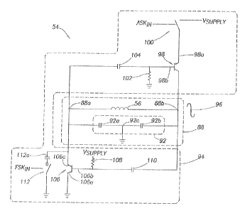
Referring to Fig. 5, in one embodiment, communication circuit 54 is formed
from a
tank circuit 88 that includes antenna 56 corulected in parallel with a
capacitor circuit 92.
6
CA 02459975 2004-03-08
Capacitor circuit 92 includes a pai;- of capacitors, shown as capacitors 92a
and 92b, which are
coupled in series. Capacitors 92a and 92b are connected in corr~mon to ground,
shown at 92c.
A feedback network 94 is also inc~uded in communication circuit 54. Feedback
network 94
is connected to selectively bias tank circuit 88 to produce one or more
signals, shown as
signal 96, at ports 88a and 88b, respectively.
Feedback network 94 incluides first and second feedback circuits. The first
feedback
circuit includes a bi-polar transistor 98, an eziiitter 98a of which is
connected to one pole of a
switch 1W The remaining poles of switch 100 are connected to VsUpj3LY and an
input
ASKIN. A base 98b of transistor 98 is connected in common with a resistor 102
and a
capacitor 104. Resistor 102 is connected in series between basc 98b and ground
92c.
Capacitor 104 is connected in series between base 98b and port 88a of tanlc
circuit 88. The
second feedback circuit includes a bi-polar transistor 106, an ernitter 106a
of which is
connected to ground. A base 106i_, of transisfor 106 is connected in common
with a resistor
108 and a capacitor 11 . Resistor 108 is connected in series between base 106b
and VsuPPLV=
A. collector 106c of transistor 106 is connected to one pole of a switeh 112
through a
capacitor 112a, with collector 106c and capacitor :"L 12a being connected in
common with port
88a of tank circuit 88. The remaining poles of switch 112 are conrtected to
ground and input
FSKIN. Capacitor 110 is connected in series between base 106b and port 88b of
tank circuit
88.
Witli this configuration antenna 56 functions as the inductor of tank eircuit
88, which
allows communication circuit 54 to always operate at a desireci resonant
frequency, i.e.
antenna 56 is always in resonance with tank circuit 88. As a result, tl:e
stabilization tirine of
communication circuit 54 is miniDnized, thereby increasing data throughput
while minimizing
the power required to transmit data. The resonant frequency of communication
;ircuit 54 is
dominated by the value of antenna 56 and capacitance circuit 92. Transistors
98 and 106 aaid
.7
CA 02459975 2004-03-08
capacitors 104 and 110 of the first and second feeciback circuit:sõ
respectiveiy, implement a
feedback loop of tank circuit 88. Specifically, each of the firsi: and, second
feedback circuits
provides 360 of feedback tc> tank circuit 88. When activated, resistor 102
forward biases
transistor 98 of the first feedback circuit, and resistor 108 forward biases
transistor 106 of the
second feedback circuit. The resu;lt is that a maximum voltage across, antenna
56 is obtained
at ports 88a and 88b, due to the 180 inversion of the signal across an.tenna
56.
Understanding that transistors 98 and 106 conduct for only a very short period
of time, the
power consumed to generate the rriaximum voltage across anterina 56 is
minimal.
The ratio CI /CZ of the values of capacitors 92a and 92b define the balance of
tarilc
circuit 88, and the amplitudes of signal 96, where =."a is the valtiP
ofca.pacitor 92a and C2 is
the value of capacitor 92b. Were the values C, and C2 substaritially equal,
tank circuit 88
operates in a balanced state and then the amplitudes of the signal across
antenna 56 would. be
substantially equal, oscillating'between ground and `Isupply. Without the
values Cr and C2
being equal, tank circuit 88 operates in an unbalanced state resulting in the
amplitude of the
signal across antenna 56 being di.fferent. Regardless, of whether tank:
circuit 88 operates in a
balanced or imbalanced state, the differential voltage level of i:he signal
across antenna 56,
measured at ports 88a and 88b, is relatively unaffected. As a result, the data
transfer power is
the same at ports 88a and 88b, i.e. power loss is minimized. Thus,
communication circuit 54
is suitable for use as both a differential mode transmitter and a common mode
receiver,
discussed more fully below
The first feedback circuit facilitates data cominunication ernploying
amplitude shift
keying (ASK) techniques. T'o that end, switch 100 is activatecl to conaiect
emitter 98a to input
ASKIN. A signal sensed at input ASKIN activates and deactivates tank circuit
88 thereby
providing the transmission current in antenna 56. In this rnanner, sigrial 96
produced by
antenna 56 is encoded to inc;ude information received at ASKIN. For example,
pressure
3
CA 02459975 2004-03-08
gauge 64, shown in Fig. 4, may trEnsmit a signal to input, A.SY;~~. "I'his
causes tank circuit 88
to transrnit signals 96 in response thereto, thereby transmitting
inforrriation obtained firom
pressure gauge 64 to a receiver (not shown) remotely disposed ~,xith respect
to
communication circuit 54. In one embodiment the information. from pressure
gauge 64 is
digital.
Alternatively, signal 96 may be encoded to contain information employing
frequency
shift keying (FSK) techniques witii the second feedback circuit, To that end,
tank circuit 88
is switched to oscillate continuousl_y using switch 11 00 to connect emirter
98a to Vsuppi;Y. A
signal, such as one generated by piessure gauge 64, may be sensed on input
FSKiN. The
signal at FSKINselectively conneci:s capacitor I 12a in parallel with
capacitor 92a, thereby
changing the resonant frequency o-Ftank circuit 88. In this manirer, signal 96
may be
produced to transmit information present at FSKIN.
Referring to Fig. 6, with minor modifications to the first feedback circuit,
communication circuit 154 may function as a receiver for signals rrzodulated
empioying; ASK
techniques. To that end, a rectifyii-ig capacitor 114 is connecte(i between
emitter 98a and
grouncl. The common connection betwee.-i emitter 98a and rectifying capacitor
114 defines
input port 116 to which a power switch could be connected anel operal:ed
remotely through
reception of a wake-up signal, as is well known in the art.
When a signal having an amplitude that is greater than t:ihe base emitter
threshold of
transistor 98 is received at port 88b, transistor 98 operates in inverse
niode. As a result,
rectifying capacitor 114 is charged througli the collector base diode of
transistor 98, when the
signal at port 88b is high. Rectifying capacitor 114 is charged 1.0 the same
voltage level
present at port 88b minus the collector base saturation voltage of transistor
98. As the
voltage level of signal 96 at port 88b drops and the voltage level of signal
96 at port 88a rises,
the voltage at base 98b becomes positive relative to che voltage at collector
1 J6c. This bias
9
CA 02459975 2004-03-08
arrangement of transistor 98 stops the collector-emitter current anct prevents
the voltage at
emitter 98a from dropping until no further signal is sensed by antenna 56.
Referring to Fig. 7, the f~..inction of comrnunication circLAt 254 may be
changed
between transmitter and receiver by coupling one pole of a stvitch 160 to
emitter 98a, with
the remaining two poles of switch 160 being coupied to VsuP~[,y and rectifying
capacitor 114.
In this manner, communication circuit 254 may function as a transrnitter by
coupling emitter
98a to VsvpPLY using switch 160 and transmitting F`SK techniques mentioned
above. T'o have
communication circuit 254 fiinction as a receiver, switch 160 is positioned to
couple ernitter
98a to rectifying capacitor 114 and operate as dYsctissed above with respect
to Fig. 6~
Referring to Fig. 8, another embodin-zent of communication circuit 354
includes an
envelope demodulator 120 connected in common with antenna 56 and capacitor
92b.
Envelope demodulator 120 includes a rectifying capacitor 122 and a resistor
124 connected in
parallel between ground and a cathode of a diode 126. An anode of diode 126 is
connected in
common with antenna 56 and capacitor 92b of tank circuit 88. Tanlc circuit 88
has greatest
sensitivity to signals sensed by antenna 56 when the values of capacitors 92a
and 92b are
selected to place tank circuit 88 in an unbalanced state, e.g., w;ith
capacitor 92a having a
value irauch greater than the value of capacitor 92b. This provi.des signal 96
at por'L 88a, with
a voltage level, relative to ground, that is rnuch larger than the voltage
level of signal 96 at
port 88b. This facilitates the detection of much smaller signals, coi-npared
to the receiver
configuration discussed above vaitIn respect to Fig. 6. If desired, a
coraparator may be
connected between the cathode of Qliode 126 and resistor 124 at point 126a to
cover the
rectified signal into a logic signalo
Referring to Fig. 9, to increase the sensitiviFy ofcommunication circuit 454
when
operating as a receiver, a matched pair diode circuit 128 connected in common
with capacitor
92b and antenna 56. Matched-pair diode circuit 128 includes an operational
amplifier ] 30
CA 02459975 2004-03-08
and first and second diodes 132a and 132b, the anodes ofwhich are connected in
common
with a coupling capacitor 134 and a bias resistor 136. A resistor 138 is
connected in series
between the cathode of diode 132b and ground, with the cathode of diode 132a
being
connected in common with an inverting input of operational atnplifier 130 and
resistor 138.
An RC network 140, which includes a resistor 140a connected in parallel with a
capacitor
140b, is connected in series betwecn grotand and a cathode of diode 132a. The
cathode of
diode 132a and RC network 140 is connected in common with a nc>n-inverting, Y,
input of
operational amplifier 130.
Referring to both Figs. 4 ar.d 9, an exemplary embodiment, the value of
resistor 138 is
slightly greater than the value of resistor 140a. In the absence of a signal
at antenna 56, a
voltage drop across diode 132a is larger than the voltage drop across diode
132b, because of a
slightly higher forward bias current. The voltage rises with the bias current.
Vvhen a signal is
sensed by antenna 56, the signal is rectified by diode 132a and not by diode
132b.
Operational amplifier 130 ignores the AC component oftl7e signal at the
inverting, V-, input.
The DC voltage at the V- input of operational amplifier 1.30 is t:illen
greater than the DC
voltage at the V'- input of operatioraal amplifier 130. As a result, the
operational aniplifier
l!.30 changes state. When the signal at antenna 56 tcrminates, capacitor 140b
discharges and
the operational amplifier 130 returris to its initial state. In this nianner,
digital signals are
produced at an output, O/P, of operational an;.plifier 130 in response to
signals sensed by
antenna 56. The signals at O/P mair be transmitted to controller circuii 60
for further
processing. By providing the match diode configuration, operational amplifier
130 may
operate at a low frequency, e.g., in the KHz range and, therefore, low
power/low bandwidth
operational amplifiers may be employed to provide significant power saving
benefits. To
increase the sensitivity of receiver circuit 128, an additional pre-anrpliiier
(not shown) niay
be connected so that capacitor 134 is connected in common to the inputs
thereof and the
11
CA 02459975 2004-03-08
output of the pre-ampli-fier (not shown) is connected in common to the anodes
of diodes 132a
and 132b.
An additional advantage with matched diode pair circuit 128 is that the same
provides
relative stability when. subjected to temperature cycling, i.e., the
differential voltage, the
voltage at the V-1 input minus the -a oltage at the V input, is relatively
independent of
temperature. The bias currents of diode I 32a and 132b are I1 and 12. The
value of capacitor
140b and resistor 138 are R.i and p.z, respectively. The ratio I1/1z ;s
defined by the ratio of
IZi/R2. As a result, the difference in the t-orward bias voltages of diodes
132a and 132b, VB,
may be defined as follows:
U,n
4~ ~U7
(1) R a = 1s (e) = ' v,~ = I (e 1I`
Rs R U!"
1r5 e 17Ui 1 5 IS. (e ~~~~~Psolving for VD from equation 1 provides the
followiiig:
(2) GV~ = r~U, ln. (1,4)
-0
P..
where fl is the emission coef'fcien~ which in the present exampie is ~ 2 for
forward biased
diodes. The variable UTis defined as follows:
(3) UT=-
q
Assuming that the operating temperature of tank circuit 88 is between 300K and
450K, we find values of UTas follows:
(4) Ul,r(300K) =~26rn.V
(5) Uz, (4 5 0.K) ~= 3 9rriV
It is desired to have the rninitnum detection input threshold voltage below
the
maximum input offset voltage. Assuming that the -iilput offset voltage of
operational
1 12
CA 02459975 2004-03-08
amplifier 130 is less than 3mV, a ratio of 1Z,/R2 may be defined as follows:
(6) AVD ~ 3rnV = 52mV ln ; R,),
R5
which yields the following:
smv
R,,
(7) - = esz~v ti 1.06,
Rs
Thus, with a 6% resistor mismatch ratio in the example shown above with
respect to
equations (1) through (7) provides V[) with a vahie of be 3mV at 300K and
4.5mV at 450K.
As shown, the differential voltage AVD is very stable over this temperature
range. The small
increase of the threshold may be a desired result, because the input offset
voltage of
operational amplifiers in general tends to rise with temperature.
Referring to both Figs. 4 and 10, communication cireuit 554 includes a voltage
multiplier circuit 142 connected to tank circuit 88. Voltage mldtiplier
circuit 142 includes a
coupling capacitor 144 connected in common with a cathode of a first diode 146
a d an
anode of a second diode 148. A rectifying capacitor 150 is connected in series
between a
cathode of second diode 148 and ground. An anode catlllode of first diode 146
is connected to
port 88a. Voltage multiplier circuit 142 increases 'che rnagnitLide of a
signal sensed by
antenna 56. When antenna 56 serises a signal, rectifying capacitor 150
charges. Once
rectifying capacitor 150 is charged, coupling capacitor 144 is ernployed to
demodulate data.
Diodes 146 and 148 rectify the signals with rectified denloduiated data being
present at
output 152, which mav be transmitted to other circuitry, such as controller
circuit 60. The
demodulated data may then be used directly with a voltage regulator. If
desired, rnaltiple
voltage multiplier circuits 142 #nay be coupled together in stages between
tank cireuit 88 and
output 152. Were rectifying capacitor 150 charged in short bursts tank circuit
88 inay be
employed to concurrently receive power and data.
Turning to Figs. 2 and 11, in operation, orice remote sensor 26 is emplaced,
it begins
13
CA 02459975 2004-03-08
collecting data. In one particular enabodirnent, remote sensor 26 includes a
timer that
periodically initiates a power up of remote sensor 216. Remote sensor 26 then
acquires data,
stores it in AI.)C/memory 66, shown in Fig. 4, and goes back to sleep. When
arrayed antenna
50 is aligned with antenna 56 of renote sensor 26, collar transmitter 162,
which contains a
power amplifier (not shown), sends a wakeup tone to remote sensor 26 through
arrayed
antenna 50. The wakeup tone is transmitted at a frequency within the bandwidth
of tank
circuit 88, shown in Fig. 10, whict, is close to the resonant frequency of
remote sensor 26.
Remote sensor 26 receives the tone throu.gl7, its antenna 56 if arrayed
antenna 50 is close
enough, detects the received si,gna'i through the receiver wakeup el.actf-
onics (not shown), and
wakes up if tlie signal is of the desired frequency. Remote sensor 26 then
sends an
acknowledge signal to collar transmitter 162 and waits to receive a command.
When awakened by collar transmitter 162. remote sensor 26 is capable of
receiving
and executing a number of commands, such as acquire data, transmit data,
memory read, and
memory write. Most commonly, collar transmitter 162 will instruct remote
sensor 26 to
ti-ansmit data. Remote sensor 26 transmits measurement data tlzrougi1 antenna
56 to
transmitter/receiver circuitry 18 aid goes back to sleep. Receiver 156 in
transmitter/receiver
circuitry 18 amplifies, demodulates and decodes the data. A duplexer 158 in
the collar
electronics protects receiver 156 in drill collar 10. Ar=rayed atrtenna 30 in
drill collar 10 is
tuned in resonance to the transmit frequency of the remote sensor 26 by, inter
alia, a tuning
circuit 164 connected between arrayed antenna 50 and duplexer 158..
More particularly, drill collar 10 is positioned in close proximity of remote
sensor 26.
In some implementations, drill collar 10 is actually used to emplace remote
sensor 26, in
which case drill collar 10 will be proximate to remote sensor 26. If remote
sensor 26 was
previously emplaced, its location may be determined from records regarding its
emplacement. As a last resort, iransceiver unit 44, shown in Fig. 3, can be
used to locate
14
CA 02459975 2004-03-08
remote sensor 26 by bobbing drill collar 10 in well bore 12. An
electromagnetic wave is
transmitted from transmitter/receiver circuitry 1S ii-I drill collar s0 to
`switeh on' remote
sensor 26 and to induce remote sensor 26 to send back an identifying coded
signal, This
` handshaking` process can be used to identify the '~ocation of rernote
sensor 26, since the
receipt of the handshaking signal from remote sensor 26 will indicate drill
collar 10 is
positioned sufficiently proximate to the location of remote sensor 26.
The location of remote sensor 26 _may be tracked once the location is
identified.
Communication between drill collar 10 at2d remote sensor 26 will typically
occur during
drilling operations, although this is not necessary to the practice of the
invention. There
typically will therefore be some degree of translational and. rotational
movement of
transceiver unit 44 relative to remote sensor 26, and this movement should be
tracked. This
can be accomplished as discussed in United States patent application number
09/899,243
entitled STEERABLE TRANSCEIVER UNIT FOR DOWNHOLE DATA ACQUISITION
IN A .FOR1ViATI N.
A handshaking process initiates the electronics of remop e sensor 26 to go
into the
acquisition and transmission mode, and pressure data and other data
representing selected
formation characteristics, as well as the sensor's identification. code, are
obtained at the level
of remote sensor 26. Note that, iri some embodirnents, remote sensor 26 might
continuously
acquire data while the transmitter is inactive, e.g. such as in the absence of
the arrayed
antenna 50. At the same tirne pressure gauge data (pressure and temperature)
and other
selected formation characteristics are acquired and the electronics of remote
sensor 26
convert the data into one or more serial digital sigaials. This digital signal
or signals, as the
case may be, is transmitted from remote sensor 26 back, to drill collar 10 via
transmitter/receiver circuitry 18. This is achieved by synchronizing and
coding each
individual bit of data into a speciaic time seqitence. Data acquisition and
transmission, or at
CA 02459975 2004-03-08
least transmission (depending on t1ie embodime-at), is ter-ininated affter
stable pressure and
temperature readings have been obtained and successfully transmitted to the on-
board
circuitry of drill collar 10.
Whenever the sequence above is initiated, transmitter/re:ceiver circuitry 18
located
within drill collar 10 is powered by transceiver power drive 46. A::
electromagnetic wave is
transmitted from drill collar 10 at a frequency determined by oscillator 48.
`The frequency
can be selected within the range from 10 KHz to 5{)1V1Hz. As sooal as remote
sensor 26
comes within the zone of influence of transmitter/receiver circuitry 18,
antenna 56 located
within remote sensor 26 will radiate back an electromagnetic wave at twice the
original
frequency by means of receiver coil control circuit 84 and antenna 56.
This concludes the detailed description of particular erribodirnents. The
particular
embodiments disclosed above are illustrative only, as the invention may be
modified and
practiced in different but equivalent manners apparent to those sk-illed in
the art having the
benefit of the teachings herein. Furthermore, no limitations are intended to
the details of
construction or design herein shown, other than as described in the claims
below. It is
therefore evident that the particular embodiments disclosed above may be
altered or modified
and that such variations are considered within the scope of the ~nvention as
claimed.
Accordingly, the protection sought herein is as set forth in the claims below.
The
embodiments of the present invention described above are exemplary. Many
changes and
modifications may be made to the disclosure recited above, while remaining
within the scope
of the invention. The scope of the invention should, therefore, be deterrnined
not with
reference to the above description, but instead should be detei-f-xzined with
reference to the
appended claims along with their full scope of equivalents.
16