Note: Descriptions are shown in the official language in which they were submitted.
CA 02460133 2004-03-09
WO 03/023692 PCT/US02/28877
SYSTEM AND METHOD FOR ENCODED SPATIO-SPECTRAL
INFORMATION PROCESSING
This application claims the priority of provisional application No.
60/318,522, filed
September 10, 2001, which is incorporated herein by reference.
FIELD OF THE INVENTION
The present invention relates generally to signal processing, and more
particularly to
devices and methods for use in spectroscopy, imaging, spatial and spectral
modulation
filtering, controllable radiation source design and related signal processing.
In another
aspect, the invention relates to methods and systems for embedding, writing,
and reading
digital information and tags in the spectral profile of ink, paint or other
materials, in order to
provide the functionality of bar codes and digital tags.
BACKGROUND OF THE INVENTION
Imagers employ either a two-dimensional (2D) multichannel detector array or a
single element detector. Imagers using a 2D detector array measure the
intensity
distribution of all spatial resolution elements simultaneously during the
entire period of data
acquisition. Imagers using a single detector require that the individual
spatial resolution
elements be measured consecutively via a raster scan so that each one is
observed for a
small fraction of the period of data acquisition. Prior art imagers using a
plurality of
detectors at the image plane can exhibit serious signal-to-noise ratio
problems. Prior art
imagers using a single element detector can exhibit more serious signal-to-
noise ratio
problems. Signal-to-noise ratio problems limit the utility of imagers applied
to chemical
imaging applications where subtle differences between a sample's constituents
become
important.
Spectrometers are commonly used to analyze the chemical composition of samples
by determining the absorption or attenuation of certain wavelengths of
electromagnetic
radiation by the sample or samples. Because it is typically necessary to
analyze the
absorption characteristics of more than one wavelength of radiation to
identify a compound,
and because each wavelength must be separately detected to distinguish the
wavelengths,
prior art spectrometers utilize a plurality of detectors, have a moving
grating, or use a set of
filter elements. However, the use of a plurality of detectors or the use of a
macro moving
grating has signal-to-noise limitations. The signal-to-noise ratio largely
dictates the ability
of the spectrometer to analyze with accuracy all of the constituents of a
sample, especially
when some of the constituents of the sample account for an extremely small
proportion of
CA 02460133 2004-03-09
WO 03/023692 PCT/US02/28877
the sample. There is, therefore, a need for imagers and spectrometers with
improved
signal-to-noise ratios.
Prior art variable band pass filter spectrometers, variable band reject filter
spectrometers, variable multiple band pass filter spectrometers or variable
multiple band
reject filter spectrometers typically employ a multitude of filters that
require macro moving
parts or other physical manipulation in order to switch between individual
filter elements or
sets of filter elements for each measurement. Each filter element employed can
be very
expensive, difficult to manufacture and all are permanently set at the time of
manufacture in
the wavelengths (bands) of radiation that they pass or reject. Physical human
handling of
the filter elements can damage them and it is time consuming to change filter
elements.
There is, therefore, a need for variable band pass filter spectrometers,
variable band reject
filter spectrometers, variable multiple band pass filter spectrometers or
variable multiple
band reject filter spectrometers without a requirement for discrete
(individual) filter
elements that have permanently set band pass or band reject properties. There
is also a need
for variable band pass filter spectrometers, variable band reject filter
spectrometers, variable
multiple band pass filter spectrometers or variable multiple band reject
filter spectrometers
to be able to change the filters corresponding to the bands of radiation that
are passed or
rejected rapidly, without macro moving parts and without human interaction.
In several practical applications it is required that an object be irradiated
with
radiation having particularly shaped spectrum. In the simplest case when only
a few
spectrum lines (or bands) are necessary, one can use a combination of
corresponding
sources, each centered near a required spectrum band. Clearly, however, this
approach does
not work in a more general case, and therefore it is desirable to have a
controllable radiation
source capable of providing arbitrary spectrum shapes and intensities. Several
types of prior
art devices are known that are capable of providing controllable radiation.
Earlier prior art
devices primarily relied upon various "masking" techniques, such as
electronically alterable
masks interposed in the optical pathway between a light source and a detector.
More recent
prior art devices use a combination of two or more light-emitting diodes
(LEDs) as radiation
sources. In such cases, an array of LEDs or light-emitting lasers is
configured for activation
using a particular encoding pattern, and can be used as a controllable light
source. A
disadvantage of these systems is that they rely on an array of different LED
elements (or
lasers), each operating in a different, relatively narrow spectrum band. In
addition, there are
technological problems associated with having an array of discrete radiation
elements with
different characteristics. Accordingly, there is a need for a controllable
radiation source,
where virtually arbitrary spectrum shape and characteristics can be designed,
and where
-2-
CA 02460133 2004-03-09
WO 03/023692 PCT/US02/28877
disadvantages associated with the prior art are obviated. Further, it is
desirable not only to
shape the spectrum of the radiation source, but also encode its components
differently,
which feature can be used to readily perform several signal processing
functions useful in a
number of practical applications. The phrase "a spectrum shape" in this
disclosure refers
not to a mathematical abstraction but rather to configurable spectrum shapes
having
ranges) and resolution necessarily limited by practical considerations.
In addition to the signal-to-noise issues discussed above, one can consider
the
tradeoff between signal-to-noise and, for example, one or more of the
following resources:
system cost, time to measure a scene, and inter-pixel calibration. Thus, in
certain prior art
systems, a single sensor system may cost less to produce, but will take longer
to fully
measure an object under study. In prior art multi-sensor systems, one often
encounters a
problem in which the different sensor elements have different response
characteristics, and
it is necessary to add components to the system to calibrate for this. It is
desirable to have a
system with which one gains the lower-cost, better signal-to-noise, and
automatic inter-pixel
calibration advantages of a single-sensor system, while not suffering all of
the time loss
usually associated with using single sensors.
Some of the problems identified above have been addressed in U.S. Pat. Nos.
6,046,808; 6,128,078 and 6,392,748 to the inventors of this application, which
are hereby
incorporated by reference.
Yet another problem in the prior art is associated with encoding of
information in
materials. The idea of using color or more generally spectral bands to
discriminate and
identify objects is known, for example in the color coding of wires, pills,
signs, as well as in
the tags used in gene arrays. But the problem with such approaches is that
encoding
information on the surface of an object is done by printing symbols, applying
bar codes and
other means that rely on: (1) generally smooth surface to permit printing
thereon; and (2) for
proper interpretation the prior art required symbols (such as letters, or bar
codes) to be
applied to an object under fairly rigid rules requiring, for example, specific
positions on the
object, orientations and shape of the symbols.
35
-3-
CA 02460133 2004-03-09
WO 03/023692 PCT/US02/28877
SUMMARY OF THE INVENTION
In one aspect, the present invention solves the above-described problems and
provides a distinct advance in the art by providing an imager or spectrometer
that is less
sensitive to ambient noise and that can effectively operate even when used in
environments
with a high level of ambient radiation. The invention further advances the art
of variable
band pass filter spectrometers, variable band reject filter spectrometers,
variable multiple
band pass filter spectrometers or variable multiple band reject filter
spectrometers by
providing a variable band pass filter spectrometer, variable band reject
filter spectrometer,
variable multiple band pass filter spectrometer or variable multiple band
reject filter
spectrometer that: (1) does not require the selection of the bands of
wavelengths passed or
rejected at the time of manufacture; (2) allows the selection of any desired
combination of
bands of wavelengths that are passed or rejected; (3) reduces the time to
change the bands of
wavelengths passed or rejected; and (4) requires no macro moving parts to
accomplish a
change in the 'bands of wavelengths passed or rejected.
In a first aspect, the system of the present invention generally includes one
or more
radiation sources, a two-dimensional array of modulateable micro-mirrors or an
equivalent
switching structure, a detector, and an analyzer. In a specific embodiment,
the two-
dimensional switching array is positioned for receiving an image. The micro-
mirrors (or
corresponding switching elements of the array) are modulated in order to
reflect individual
spatially-distributed radiation components of the image toward the detector.
In a preferred
embodiment, the modulation is performed using known and selectively different
modulation
rates.
According to this aspect of the invention, a detector is oriented to receive
the
combined radiation components reflected from the array and is operable to
generate an
output signal representative of the combined radiation incident thereon. The
analyzer is
operably coupled with the detector to receive the output signal and to
demodulate the signal
to recover signals representative of each of the individual spatially
distributed radiation
components of the image. The analyzer can be configured to recover all
reflected
components or to rej ect some umlecessary components of the recovered signals
from the
combined reflections.
By using micro-mirrors that receive the individual spectral or spatial
radiation
components and then modulate these components at different modulation rates,
all of the
radiation components can be focused onto a single detector and then
demodulated to
maximize the signal-to-noise ratio (SNR) of the detector. Various techniques
for enhancing
the SNR of the system are presented as well.
-4-
CA 02460133 2004-03-09
WO 03/023692 PCT/US02/28877
In another important aspect, the present invention provides a distinct advance
in the
state of the art by enabling the design of a controllable radiation source,
which uses no
masking elements, which are generally slow and cumbersome to operate, and no
discrete
light sources, which also present a number of technical issues in practice.
Instead, the
controllable radiation source in accordance with a preferred embodiment is
implemented
using a broadband source illuminating a two-dimensional array of switching
elements, such
as a DMA. Modulation of the individual switching elements of the array
provides an easy
mechanism for spatio-spectral encoding of the input radiation, which encoding
can be used
in a number of practical applications.
In accordance with another aspect of the invention, a two-dimensional array of
switching elements, such as a DMA, can be configured and used as a basic
building block
for various optical processing tasks, and is referred to as an optical synapse
processing unit
(OSPU). Combinations of OSPUs with standard processing components can be used
in the
preferred embodiments of the present invention in a number of practical
applications,
including data compression, feature extraction and others. In a specific
embodiment, a
spectrometer using a controlled radiation source provides for very rapid
analysis of a sample
using an orthogonal set of basis functions, such as Hadamard or Fourier
transform
techniques, resulting in significantly enhanced signal-to-noise ratio.
The present invention gains the lower-cost, better signal-to-noise, and
automatic
inter-pixel calibration advantages of single-sensor systems, while not
suffering all of the
time loss usually associated with using single sensors, because it allows for
adaptive and
tunable acquisition of only the desired information, as opposed to prior-art
systems which
are generally full data-cube acquisition devices requiring additional post
processing to
discover or recover the knowledge ultimately sought in the application of the
system.
One skilled in the art will recognize that, while the invention here is
described using 2D
arrays of micro-mirrors, any 2D spatial light modulator can be used. It should
also be noted
that a pair, or a few 1 D spatial light modulators can be combined to
effectively produce a
2D spatial light modulator for applications that involve raster scanning,
Walsh-Hadamard
scanning, or scanning or acquisition with any separable library of patterns.
It is intended that the devices and methods in this application in general are
capable
of operating in various ranges of electromagnetic radiation, including the
ultraviolet, visible,
infrared, and microwave spectrum portions. Further, it will be appreciated by
those of skill
in the art of signal processing, be it acoustic, electric, magnetic, etc.,
that the devices and
techniques disclosed herein for optical signal processing can be applied in a
straight-
forward way to those other signals as well.
-5-
CA 02460133 2004-03-09
WO 03/023692 PCT/US02/28877
In another important aspect, the invention provides systems and methods for
encoded spatio-spectral information processing. In a specific aspect aspect,
the invention
involves applying or embedding of digital information in the spectral profile
of materials,
such as inks and paints, to provide the functionality of bar codes or labels,
and reading such
information from objects. Recording of digital information is enabled onto or
into physical
media with or without the use of printed symbols, by spraying, mixing or
enabling a specific
chemical changes resulting in digital information being encoded onto or into
carrying
materials. Because the information is encoded in the spectral signatures of
compositions of
materials, the precise location, shape, orientation and arrangement of marks
is generally not
used in the process of decoding.
Accordingly, in this aspect the invention is a method for encoding
information,
comprising the steps of: providing two or more materials capable of reacting
predictably to
one or more radiation components in a given spectral range; selecting a
combination of the
two or more materials, the selected combination having a spectral response
signature in the
given spectral range corresponding to one of a plurality of distinct values
associated with a
predetermined encoding algorithm; and applying the combination of materials to
an object
in one or more marks, the specific position, arrangement, orientation and
shape of a mark
with respect to the object or to other marks not being part of the encoding
algorithm.
BRIEF DESCRIPTION OF THE DRAWINGS
The present invention will be understood and appreciated more fully from the
following detailed description, taken in conjunction with the drawings in
which:
FIGS. 1A and 1B are schematic diagrams illustrating a spectrometer constructed
in
accordance with two embodiments of the invention;
FIG. 2 is a plan view of a micro-mirror array used in the present invention;
FIG. 3 is a schematic diagram of two micro-mirrors illustrating the
modulations of
the mirrors of the micro-mirror device of FIG. 2;
FIG. 4 is a graph illustrating an output signal of the spectrometer when used
to
analyze the composition of a sample;
FIG. 5 is a graph illustrating an output signal of the imager when used for
imaging
purposes;
FIG. 6 is a schematic diagram illustrating an imager constructed in accordance
with
a preferred embodiment of the invention; FIG. 6A illustrates spatio-spectral
distribution of a
DMA, where individual elements can be modulated;
-6-
CA 02460133 2004-03-09
WO 03/023692 PCT/US02/28877
FIG. 7 is an illustration of the input to the DMA Filter Spectrometer and its
use to
pass or reject wavelength of radiation specific to constituents in a sample;
FIG. 8 illustrates the design of a band pass filter in accordance with the
present
invention (top portion) and the profile of the radiation passing through the
filter (bottom
portion);
FIG. 9 illustrates the design of mufti-modal band-pass or band-reject filters
with
corresponding intensity plots, in accordance with the present invention;
FIG. 10 illustrates the means for the intensity variation of a spectral filter
built in
accordance with this invention;
FIGs 11-14 illustrate alternative embodiments of a modulating spectrometer in
accordance with this invention; FIGS. 11 A and 11 B show embodiments in which
the DMA
is replaced with concave mirrors; FIG. 12 illustrates an embodiment of a
complete
modulating spectrometer in which the DMA element is replaced by the concave
mirrors of
FIG. 11. Figure 13 illustrates a modulating lens spectrometer using lenses
instead of DMA,
and a "barber pole" arrangement of mirrors to implement variable modulation.
FIG. 14.
illustrates a "barber pole" modulator arrangement;
FIGS. 15 and 16 illustrate an embodiment of this invention in which one or
more
light sources provide several modulated spectral bands using a fiber optic
bundle;
FIG. 17 illustrates in diagram form an apparatus using controllable radiation
source;
FIGS. 18A and 18B illustrate in a diagram form an optical synapse processing
unit
(OSPU) used as a processing element in accordance with the present invention;
FIG. 19 illustrates in a diagram form the design of a spectrograph using OSPU;
FIG. 20 illustrates in a diagram form an embodiment of a tunable light source;
FIG. 21 illustrates in a diagram form an embodiment of the spectral imaging
device,
which is built using two OSPUs;
FIGs. 22 and 23 illustrate different devices built using OSPUs;
FIGS 24-26 are flow charts of various scans used in accordance with the
present
invention. Specifically, FIG. 24 is a flow chart of a raster-scan used in one
embodiment of
the present invention; FIG. 25 is a flowchart of a Walsh-Hadamard scan used in
accordance
with another embodiment of the invention. FIG. 26 is a flowchart of a mufti-
scale scan, used
in a different embodiment; Fig. 26A illustrates a mufti-scale tracking
algorithm in a
preferred embodiment of the present invention;
FIG. 27 is a block diagram of a spectrometer with two detectors;
FIG. 28 illustrates a Walsh packet library of patterns for N = 8.
-7_
CA 02460133 2004-03-09
WO 03/023692 PCT/US02/28877
FIG. 29 is a generalized block diagram of hyperspectral processing in
accordance
with the invention;
FIG. 30 illustrates the difference in two spectral components (red and green)
of a
data cube produced by imaging the same object in different spectral bands;
FIG. 31A-E illustrate different embodiments of an imaging spectrograph used in
accordance with this invention in de-dispersive mode;
FIG. 32 shows an axial and a cross-sectional views of a fiber optic assembly;
FIG. 33 shows a physical arrangement of the fiber optic cable, detector and
the slit;
FIG. 34 illustrates a fiber optic surface contact probe head abutting tissue
to be
examined;
FIG. 35 A and 35 B illustrate a fiber optic e-Probe for pierced ears that can
be used
for medical monitoring applications in accordance with the present invention;
FIGs. 36A, 36B and 36C illustrate different configurations of a hyperspectral
adaptive wavelength advanced illuminating imaging spectrograph (HAWAIIS) in
accordance with this invention;
FIG. 37 illustrates a DMA search by splitting the scene;
FIG. 38 illustrates wheat spectra data (training) and wavelet spectrum in an
example
of determining protein content in wheat;
FIG. 39 illustrates the top 10 wavelet packets in local regression basis
selected using
50 training samples in the example of FIG. 38; FIG 40 is a scatter plot of
protein content
(test data) vs. correlation with top wavelet packet; Fig 41 illustrates PLS
regression of
protein content of test data;
FIG. 42 illustrates the advantage of DNA-based Hadamard Spectroscopy used in
accordance with the present invention over the regular raster scan;
FIGS. 43, 44, 45, 46 and 47(A-D) illustrate hyperspectrum processing in
accordance
with the present invention;
FIG. 48 illustrates a system for topological application of encoded
information, in
accordance with a preferred embodiment;
FIG. 49 illustrates an object containing information encoded in a collection
of
marks, in accordance with the invention. The illustrated marks are of the
"bull's-eye"
pattern, where each mark consists of concentric rings of encoded material;
FIG. 50 illustrates a specific example where the topological application of
marks on
a rough or variegated surface creates ambiguity about the relative placement
of the marks,
depending on viewing angle, so that spectral marking according to the present
invention is
_g_
CA 02460133 2004-03-09
WO 03/023692 PCT/US02/28877
advantageous, in order to recover the ordering of the marks by decoding the
information
stored in the marks.
FIG. 51 depicts a compact reader in accordance with one embodiment of the
present
invention, in which a spectrally modulatable light source and a detector are
contained in a
reading "wand" that can be waived across a mark to read its spectral content.
15
25
35
-9-
CA 02460133 2004-03-09
WO 03/023692 PCT/US02/28877
DETAILED DESCRIPTION OF THE PREFERRED EMBODIMENTS
In one aspect, the present invention concerns the analysis of radiation
passing
through or reflected from a sample of a material of interest. Since signal
processing in this
aspect of the invention is performed after the sample has been irradiated, in
the disclosure in
Section I below it is referred to as post-sample processing. Section II deals
with the aspect
of the invention in which radiation has already been processed prior to its
interaction with
the sample (e.g. based on a priori knowledge), and is accordingly referred to
as pre-sample
processing. Various processing teclnuques applicable in both pre-sample and
post-sample
processing are considered in Section III. Finally, Section IV illustrates the
use of the
proposed techniques and approaches in the description of various practical
applications.
I. POST-SAMPLE PROCESSING
A. The Basic System
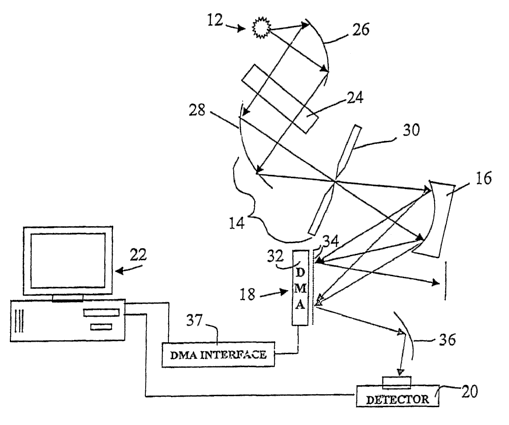
Turning now to the drawing figures and particularly Fig. 1A and 1B, a
spectrometer
assembly 10 constructed in accordance with one embodiment of the invention is
illustrated.
With reference to Fig. 1A the device broadly includes a source 12 of
electromagnetic
radiation, a mirror and slit assembly 14, a wavelength dispersing device 16, a
spatial light
modulator 18, a detector 20, and an analyzing device 22.
In particular, the electromagnetic radiation source 12 is operable to project
rays of
radiation onto or through a sample 24 that is to be analyzed, such as a sample
of body tissue
or blood. The radiation source may be any device that generates
electromagnetic radiation
in a known wavelength spectrum such as a globar, hot wire, or light bulb that
produces
radiation in the infrared spectrum. To increase the amount of rays that are
directed to the
sample, a parabolic reflector 26 may be interposed between the source 12 and
the sample
24. In a specific embodiment, the source of electromagnetic radiation is
selected as to yield
a continuous band of spectral energies, and is referred to as the source
radiation. It should
be apparent that the energies of the radiation source are selected to cover
the spectral region
of interest for the particular application.
The mirror and slit assembly 14 is positioned to receive the radiation rays
from the
source 12 after they have passed through the sample 24 and is operable to
focus the
radiation onto and through an entrance slit 30. The collection mirror 28
focuses the
radiation rays through slit 30 and illuminates the wavelength dispersing
device 16. As
shown in diagram form in Fig. 1B, in different embodiments of the invention
radiation rays
- 10-
CA 02460133 2004-03-09
WO 03/023692 PCT/US02/28877
from the slit may also be collected through a lens 15, before illuminating a
wavelength
dispersion device 16.
The wavelength dispersing device 16 receives the beams of radiation from the
mirror and slit assembly 14 and disperses the radiation into a series of lines
of radiation
each corresponding to a particular wavelength of the radiation spectrum. The
preferred
wavelength dispersing device is a concave diffraction grating; however, other
wavelength
dispersing devices, such as a prism, may be utilized. In a specific
embodiment, the
wavelengths from the dispersing device 16 are in the near infrared portion of
the spectrum
and may cover, for example, the range of 1650-1850 nanometers (nm). It should
be
emphasized, however, that in general this device is not limited to just this
or to any spectral
region. It is intended that the dispersion device in general is capable of
operating in other
ranges of electromagnetic radiation, including the ultraviolet, visible,
infrared, and
microwave spectrum portions, as well as acoustic, electric, magnetic, and
other signals,
where applicable.
The spatial light modulator (SLM) 18 receives radiation from the wavelength
dispersing device 16, individually modulates each spectral line, and reflects
the modulated
lines of radiation onto the detector 20. As illustrated in Fig. 2, the SLM is
implemented in a
first preferred embodiment as a micro-mirror array that includes a semi-
conductor chip or
piezo-electric device 32 having an array of small reflecting surfaces 34
thereon that act as
mirrors. One such micro-mirror array is manufactured by Texas Instruments and
is
described in more detail in U.S. Pat. No. 5,061,049, hereby incorporated into
the present
application by reference. Those skilled in the art will appreciate that other
spatial light
modulators, such as a magneto-optic modulator or a liquid crystal device may
be used
instead of the micro-mirror array. Various embodiments of such devices are
discussed in
more detail below.
The semi-conductor 32 of the micro-mirror array 18 is operable to individually
tilt
each mirror along its diagonal between a first position depicted by the letter
A and a second
position depicted by the letter B in Fig. 3. In preferred forms, the semi-
conductor tilts each
mirror 10 degrees in each direction from the horizontal. The tilting of the
mirrors 34 is
preferably controlled by the analyzing device 22, which may communicate with
the
micro-mirror array 18 through an interface 37.
The micro-mirror array 18 is positioned so that the wavelength dispersing
device 16
reflects each of the lines of radiation upon a separate column or row of the
array. Each
column or row of mirrors is then tilted or wobbled at a specific and separate
modulation
-11-
CA 02460133 2004-03-09
WO 03/023692 PCT/US02/28877
frequency. For example, the first row of mirrors may be wobbled at a
modulation frequency
of 100 Hz, the second row at 200 Hz, the third row at 300 Hz, etc.
In a specific embodiment, the mirrors are calibrated and positioned so that
they
reflect all of the modulated lines of radiation onto a detector 20. Thus, even
though each
column or row of mirrors modulates its corresponding line of radiation at a
different
modulation frequency, all of the lines of radiation are focused onto a single
detector.
The detector 20, which may be any conventional radiation transducer or similar
device, is oriented to receive the combined modulated lines of radiation from
the
micro-mirror array 18. The detector is operable for converting the radiation
signals into a
digital output signal that is representative of the combined radiation lines
that are reflected
from the micro-mirror array. A reflector 36 may be interposed between the
micro-mirror
array 18 and the detector 20 to receive the combined modulated lines of
radiation from the
array and to focus the reflected lines onto the detector.
The analyzing device 22 is operably coupled with the detector 20 and is
operable to
receive and analyze the digital output signal from the detector. The analyzing
device uses
digital processing techniques to demodulate the signal into separate signals
each
representative of a separate line of radiation reflected from the micro-mirror
array. For
example, the analyzing device may use discrete Fourier transform processing to
demodulate
the signal to determine, in real time, the intensity of each line of radiation
reflected onto the
detector. Thus, even though all of the lines of radiation from the micro-
mirror array are
focused onto a single detector, the analyzing device can separately analyze
the
characteristics of each line of radiation for use in analyzing the composition
of the sample.
In accordance with one embodiment of this invention, the analyzing device is
preferably a computer that includes spectral analysis software. Fig. 4
illustrates an output
signal generated by the analyzing device in accordance with one embodiment.
The output
signal illustrated in Fig. 4 is a plot of the absorption characteristics of
five wavelengths of
radiation from a radiation source that has passed through a sample.
In one embodiment of the system of this invention illustrated in Fig. 6A, it
is used
for digital imaging purposes. In particular, when used as an imaging device,
an image of a
sample 38 is focused onto a micro-mirror array 40 and each micro-mirror in the
array is
modulated at a different modulation rate. The micro-mirror array geometry is
such that
some or all of the reflected radiation impinges upon a single detector element
42 and is
subsequently demodulated to reconstruct the original image improving the
signal-to-noise
ratio of the imager. Specifically, an analyzing device 44 digitally processes
the combined
signal to analyze the magnitude of each individual pixel. FIG. 6B illustrates
spatio-spectral
-12-
CA 02460133 2004-03-09
WO 03/023692 PCT/US02/28877
distribution of the DMA, where individual elements can be modulated. Fig. 5 is
a plot of a
three dimensional image showing the magnitude of each individual pixel.
Fig. 7 illustrates the output of a digital micro-mirror array (DMA) filter
spectrometer
used as a variable band pass filter spectrometer, variable band reject filter
spectrometer,
variable multiple band pass filter spectrometer or variable multiple band
reject filter
spectrometer. In this embodiment, the combined measurement of the
electromagnetic
energy absorbed by sample constituents A and C is of interest. The shaded
regions in Fig. 7
illustrate the different regions of the electromagnetic spectrum that will be
allowed to pass
to the detector by the DMA filter spectrometer. The wavelengths of
electromagnetic
radiation selected to pass to the detector correspond to the absorption band
for compound A
and absorption band for compound C in a sample consisting of compounds A, B,
and C.
The spectral region corresponding to the absorption band of compound B and all
other
wavelengths of electromagnetic radiation are rejected. Those skilled in the
art will
appreciate that the DMA filter spectrometer is not limited to the above
example and can be
used to pass or reject any combination of spectral resolution elements
available to the DMA.
Various examples and modifications are considered in detail below.
As a DMA filter imager the spatial resolution elements (pixels) of an image
can be
selectively passed or rejected (filtered) according to the requirements of the
image
measurement. The advantages of both the DMA filter spectrometer and DMA filter
imager
are:
(1) All spectral resolution elements or spatial resolution elements
corresponding to
the compounds of interest in a particular sample can be directed
simultaneously to the
detector for measurement. This has the effect of increasing the signal-to-
noise ratio of the
measurement.
(2) The amount of data requiring processing is reduced. This reduces storage
requirements and processing times.
B. Modulated Spectral Filter Design
(i) Design Basics
The preceding section described the components of the basic system used in
accordance with the present invention, and their operation. The focus of this
section is on
the design of specific modulated spectral filters using the spatial light
modulator (SLM) 18,
which in a preferred embodiment is implemented using a digital micro-mirror
array (DMA).
As noted above, using a DMA one can provide one or more spectral band pass or
band-reject filters) with a chosen relative intensity. In particular, in
accordance with the
-13-
CA 02460133 2004-03-09
WO 03/023692 PCT/US02/28877
present invention the radiation wavelengths that are reflected in the
direction of the detector
are selected by specific columns of micro-mirrors of the DMA, as illustrated
in Fig. 8. The
relative intensity of the above spectral band is controlled by the selection
of specific area of
micro-mirrors on the DMA, represented by the dark area designated "A" in Fig.
8. Thus,
the dark area shown in Fig. 8 is the mirrors that direct specific wavelength
radiation, i.e.,
spectral band, to the detector. Clearly, the "on" mirrors in the dark area
create a band-pass
filter, the characteristics of which are determined by the position of the
"on" area in the
DMA. The bottom portion of the figure illustrates the profile of the radiation
reaching the
detector.
Fig.8 also demonstrates the selection of specific rows and columns of mirrors
in the
DMA used to create one spectral band filter with a single spectral mode. It
should be
apparent, however, that using the same technique of blocking areas in the DMA
one can
obtain a plurality of different specific spectral band filters, which can have
multi-modal
characteristics. The design of such filters is illustrated in Fig. 9.
As shown in Fig. 9, a multitude of different specific filters can be designed
on one
DMA using simple stacking. Fig. 9 illustrates the creation of several filters
by selective
reflection from specific micro-mirrors. In particular, the left side of the
figure illustrates the
creation of three different filters, designated 1, 2, and 3. This is
accomplished by the
selection of specific mirrors on the DMA, as described above with reference to
Fig. 8. The
total collection of spectral band filters is shown at the bottom-left of this
figure. The
spectral band provided by each filter is shown on the right-hand side of the
figure. The
bottom right portion illustrates the radiation passing through the combination
of filters 1, 2
and 3.
The above discussion describes how the relative intensity of each spectral
band can
be a function of the DMA area used in the reflection. The following table
illustrates the
linear relationship between areas of the DMA occupied by individual filters,
and the
resulting filter. Clearly, if the entire DMA array is in the "on" position,
there will be no
filtering and in principle the input radiation passes through with no
attenuation.
Figure 9, left side Figure 9, right side
Reflected radiation from micro-mirrors Filter created
area A 1
area B 2
area C 3
areas a+b+c 1 +2+3
- 14-
CA 02460133 2004-03-09
WO 03/023692 PCT/US02/28877
Figure 10 illustrates the means for the intensity variation of a spectral
filter built in
accordance with this invention, and is summarized in the table below.
Example A Example B
Reflection from a DMA The intensity recorded at the
detector for
See Figs. 8 and 9. example A for the combination
filter 1, 2,
Reflection areas 1, 2, and and 3, Intensity, I, h = IZ
3 create spectral = I3
filter 1, 2 and 3 respectively.
area 1 = area 2 = area 3
Example C Example D
The reflection of area 2 of The intensity recorded at the
the DMA is detector for
increased. filters 1, 2, and 3 is
area 1 = area 3 < area 2 h ~ I3 < IZ
Example F
Example E
The intensity recorded at the
detector for
The reflection of axes 2 of filter 1, 2, and 3 is
the DMA is
decreased h = I3 < IZ
area 1 = area 3 < area 2
(ii) Modulation
Figures 9 and 10 illustrate the ability to design spectral filters with
different
characteristics using a DMA. The important point to keep in mind is that
different spectral
components of the radiation from the sample have been separated in space and
can be
filtered individually. It is important to retain the ability to process
individual spectral
components separately. To this end, in accordance with the present invention,
spectral
components are modulated.
The basic idea is to simply modulate the output from different filters
differently, so
one can identify and process them separately. In a preferred embodiment,
different
modulation is implemented by means of different modulation rates. Thus, with
reference to
30 Fig. 9,. the output of filter 1 is modulated at rate Ml; output of filter 2
is modulated at rate
M~, and filter 3 is modulated using rate M3, where Ml ~ MZ ~ M3. In different
embodiments, modulation may be achieved by assigning a different modulation
encodement
to each filter, with which it is modulated over time.
-15-
CA 02460133 2004-03-09
WO 03/023692 PCT/US02/28877
As a result, a system built in accordance with the present invention is
capable of
providing: a) Spectral bandwidth by selection of specific columns of micro-
mirrors in an
array; b) Spectral intensity by selection of rows of the array; and c)
Spectral band
identification by modulation. All of the above features are important in
practical
applications, as discussed in Section IV below.
C. Alternative Embodiments
(i) Modulating Spectrometers without a DMD.
Figures 11-14 illustrate alternative embodiments of a modulating spectrometer
in
accordance with this invention, where the DMA is replaced with different
components. In
particular, Fig. 11A and B show an embodiment in which the DMA is replaced
with fixed
elements, in this case concave mirrors. The idea is to use fixed spectral
grating, which
masks out spectnun block components that are not needed and passes those which
are.
The idea here is that the broadly illuminated dispersive element distributes
spectral
resolution elements in one dimension so that in the orthogonal dimension one
can collect
light of the same wavelengths. With reference to Fig. 6A one can see that at a
particular
defined plane, herein called the focal plane, one has a wavelength axis(x or
columns) and a
spatial axis(y or rows). If one were to increase the number of spatial
resolution elements (y)
that are allowed to pass energy through the system and out of the exit
aperture for any given
wavelength (x), or spectral resolution element (x), this would have the effect
of increasing
the intensity of the particular spectral resolution elements' intensity at the
detector.
If the array of spatio/spectral resolution elements at the focal plane as
shown in Fig.
6A is replaced with fixed elements, such as the concave mirrors in Fig. 11B,
one can have a
different device configured to perform a particular signal processing task -
in this case pass
the predetermined spectrum components at the desired intensity levels. Fig.
11A shows the
spatio/spectral resolution elements at the focal plane to be used. The fixed
optical elements
are placed to interact with predetermined spatio/spectral resolution elements
provided by the
grating and entrance aperture geometry and to direct the specific assortment
of
spatio/spectral elements to specific spatial locations for modulation encoding
(possibly
using the barber pole arrangement, shown next).
Fig. 12 illustrates an embodiment of a complete modulating spectrometer in
which
the DMA element is replaced by the concave mirrors of Fig. 11. Figure 13
illustrates a
modulating lens spectrometer using lenses instead of DMA, and a "barber pole"
arrangement of mirrors to implement variable modulation. The "barber pole"
modulation
arrangement is illustrated in Fig. 14.
- 16-
CA 02460133 2004-03-09
WO 03/023692 PCT/US02/28877
With reference to Fig. 14, modulation is accomplished by rotating this "barber
pole"
that has different number of mirrors mounted for reflecting light from the
spatially separated
spectral wavelengths. Thus, irradiating each vertical section will give the
reflector its own
distinguishable frequency. In accordance with this embodiment, light from the
pole is
collected and simultaneously sent to the detector. Thus, radiation from
concave mirror 1
impinges upon the four-mirror modulator; concave mirror 2 radiation is
modulated by the
five-mirror modulator, and concave mirror 3 directs radiation to the six-
mirror modulator.
In the illustrated embodiment, the modulator rate is four, five, or six times
per revolution of
the "barber pole."
The operation of the device is clarified with reference to Fig. 12, tracing
the
radiation from the concave mirrors 12 to the detector of the system. In
particular, concave
mirror 1 reflects a selected spectral band with chosen intensity. This
radiated wave
impinges upon a modulator, implemented in this embodiment as a rotation barber
pole. The
modulating rates created by the barber pole in the exemplary embodiment shown
in the
figure are as shown in the table below.
Number of mirrors Modulation
Figure 13 Per 360 rotation Per 360 of barber
pole
Area A 4 4/360
Area B 5 5/360
Area C 6 6/360
Accordingly, this arrangement yields a modulation rate of 4/360° for
the radiation from
Area A, Figure 12.
By a analogy, the mirrors of Areas B and C are modulated at the rate of
5/360° and
6/360°, respectively. As illustrated, all radiation from mirrors A, B,
and C is
simultaneously directed to the detector. This radiation is collected by either
a simple mirror
lens or a toroidal mirror, which focuses the radiation onto a single detector.
The signal from
the detector now goes to electronic processing and mathematical analyses for
spectroscopic
results.
(ii) Modulating Light Sources Spectrometer.
In the discussion of modulating spectrometers, a single light source of
electromagnetic radiation was described. There exist yet another possibility
for a unique
3 5 optical design - a modulating multi-light source spectrometer. Figs. 15
and 16 illustrate an
-17-
CA 02460133 2004-03-09
WO 03/023692 PCT/US02/28877
embodiment of this invention in which a light source 12 provides several
modulated
spectral bands, e.g., light emitting diodes (LED), or lasers (shown here in
three different
light sources). The radiation from these light sources impinges upon the
sample 24. One
possible illumination design is one in which light from a source, e.g. LED,
passes through a
multitude of filters, impinging upon the sample 24. The radiation from the
sample is
transmitted to a detector 20, illustrated as a black fiber. The signal from
the detector is
electronically processed to a quantitative and-qualitative signal describing
the sample
chemical composition.
In this embodiment, a plurality of light sources is used at differed
modulating rates.
Fig. 15 and 16 illustrate the combination of several light sources in the
spectrometer. The
choice of several different spectral bands of electromagnetic radiation can be
either light
emitting diodes, LED, lasers, black body radiation and/or microwaves.
Essentially the
following modulation scheme can be used to identify the different light
sources, in this
example LED's of different spectral band wavelength.
No. of Spectral band Modulation
Source Wavelength, nm Rate
1 1500-1700 ml
2 1600-1800 m~
3 1700-1900 m3
Note: ml ~ m2 ~ m3 ~ ...
It should be noted that either the radiation will be scattered or transmitted
by the
sample 24. This scattered or transmitted radiation from the sample is
collected by an optical
fiber. This radiation from the sample is conducted to the detector. The signal
from the
detector is electronically processed to yield quantitative and qualitative
information about
the sample.
In a particular embodiment the radiation path consists of optical fibers.
However, in
accordance with alternate embodiments, mirrors and lenses could also
constitute the optical
path for a similar modulating mufti-light source spectrometer.
(iii) Modulating Mufti-source Hyperspectral Imaging Spectrometer
The spectrometer described in the preceding section records spectral
information
about one unique area on a single detector. In a similar manner, the spectral
characteristic
of a multitude of areas in a sample can be recorded with a multitude of
detectors in
accordance with different embodiments of the invention. Such a multitude of
detectors
exists in an array detector. Array detectors are known in the art and include,
for example
-18-
CA 02460133 2004-03-09
WO 03/023692 PCT/US02/28877
Charge coupled devices (CCD), in the ultraviolet, and visible portions of the
spectrum; InSb - array in near infrared; InGaAs - array in near infrared; Hg-
Cd-Te - array
in mid-infrared and other array detectors.
Array detectors can operate in the focal plane of the optics. Here each
detector of
the array detects and records the signal from a specific area, x;y;. Practical
Example B in
Section IV on the gray-level camera provides a further illustration. Different
aspects of the
embodiments discussed in sections (iii) and (iv) are considered in more detail
in the
following sections. As is understood by one skilled in the art, standard
optical duality
implies that each of the preceding configurations can be operated in reverse,
exchanging the
position of the source and the detector.
II. PRE-SAMPLE PROCESSING
The preceding section described an aspect of the invention referred to as post-
sample processing, i.e., signal processing performed after a sample had been
irradiated. In
accordance with another important aspect of this invention, significant
benefits can result
from irradiating a sample with pre-processed radiation, in what is referred to
as pre-sample
processing. Most important in this context is the use, in accordance with this
invention, of
one or more light sources, capable of providing modulated temporal and/or
spatial patterns
of input radiation. These sources are referred to next as controllable
sources) of radiation,
which in general are capable of generating arbitrary combinations of spectral
radiation
components within a predetermined spectrum range.
Several types of prior art devices axe known that are capable of providing
controllable radiation. Earlier prior art devices primarily relied upon
various "masking"
techniques, such as electronically alterable masks interposed in the optical
pathway between
a light source and a detector. More recent prior art devices use a combination
of two or
more light-emitting diodes (LEDs) as radiation sources. Examples are provided
in U.S. Pat.
Nos. 5,257,086 and 5,488,474, the content of which is hereby incorporated by
reference for
all purposes. As discussed in the above patents, an array of LEDs or light-
emitting lasers is
configured for activation using a particular encoding pattern, and can be used
as a
controllable light source. A disadvantage of this system is that it relies on
an array of
different LED elements, each operating in a different, relatively narrow
spectrum band. In
addition, there are technological problems associated with having an array of
discrete
radiation elements with different characteristics.
-19-
CA 02460133 2004-03-09
WO 03/023692 PCT/US02/28877
These and other problems associated with the prior art are addressed in
accordance
with the present invention using a device that in a specific embodiment can be
thought of as
the reverse of the setup illustrated in Fig. 1A. In particular, one or more
broadband
radiation sources illuminate the digital micro-mirror array (DMA) 18 and the
modulations
of the micro-mirrors in the DMA encode the source radiation prior to impinging
upon the
sample. The reflected radiation is then collected from the sample and directed
onto a
detector for further processing.
Fig. 17 illustrates a schematic representation of an apparatus in accordance
with the
present invention using a controllable radiation source. Generally, the system
includes a
broadband radiation source 12, DMA 18, wavelength dispersion device 16, slit
assembly 30,
detector 20 and control assembly 22.
In particular, control assembly 22 may include a conventional personal
computer
104, interface 106, pattern generator 108, DMA driver 110, and analog to
digital (A/D)
converter 114. Interface 106 operates as a protocol converter enabling
communications
between the computer 22 and devices 108-114.
Pattern generator 108 may include an EPROM memory device (not shown) which
stores the various encoding patterns for array 18, such as the Hadamard
encoding pattern
discussed below. In response to control signals from computer 22, generator
108 delivers
signals representative of successive patterns to driver 110. More
particularly, generator 108
produces output signals to driver 110 indicating the activation pattern of the
mirrors in the
DMA 18. A/D converter 114 is conventional in nature and receives the voltage
signals
from detector 20, amplifies these signals as analog input to the converter in
order to produce
a digital output representative of the voltage signals.
Radiation source 12, grating 16, DMA 18 slit assembly 30 and detector 20
cooperatively define an optical pathway. Radiation from source 12 is passed
through a
wavelength dispersion device, which separates in space different spectrum
bands. The
desired radiation spectrum can them be shaped by DMA 18 using the filter
arrangement
outlined in Section I(B)(i). In accordance with a preferred embodiment,
radiation falling on
a particular micro-mirror element can also be encoded with a modulation
pattern applied to
it. In a specific mode of operating the device, DMA 18 is activated to reflect
radiation in a
successive set of encoding patterns, such as Hadamard, Fourier, wavelet or
others. The
resultant set of spectral components is detected by detector 20, which
provides
corresponding output signals. Computer 22 then processes these signals.
Computer 22 initiates an analysis by prompting pattern generator 108 to
activate the
successive encoding patterns. With each pattern, a set of wavelength
components are
-20-
CA 02460133 2004-03-09
WO 03/023692 PCT/US02/28877
resolved by grating 16 and after reflection from the DMA 18 is directed onto
detector 20.
Along with the activation of encoding patterns, computer 22 also takes
readings from A/D
converter 114, by sampling data. These readings enable computer 22 to solve a
conventional inverse transform, and thereby eliminate background noise from
the readings
for analysis.
In summary, the active light source in accordance with the present invention
consists
of one or more light sources, from which various spectral bands are selected
for
transmission, while being modulated with a temporal and/or spatial patterns.
The resulting
radiation is then directed at a region (or material) of interest to achieve a
variety of desired
tasks. A brief listing of these tasks include: (a) Very precise spectral
coloring of a scene, for
purposes of enhancement of display and photography; (b) Precise illumination
spectrum to
correspond to specific absorption lines of a compound that needs to be
detected, (see figures
40-44 on protein in wheat as an illustration) or for which it is desirable to
have energy
absorption and heating, without affecting neighboring compounds (This is the
principle of
the microwave oven for which the radiation is tuned to be absorbed by water
molecules
allowing for heating of moist food only); (c) The procedure in (b) could be
used to imprint a
specific spectral tag on ink or paint, for watermarking, tracking and forgery
prevention,
acting as a spectral bar code encryption; (d) The process of light curing to
achieve selected
chemical reactions is enabled by the tunable light source.
Various other applications are considered in further detail in Section IV.
Duality
allows one to reverse or "turn inside out" any of the post-sample processing
configurations
described previously, to yield a pre-sample processing configuration.
Essentially, in the
former case one takes post sample light, separates wavelengths, encodes or
modulates each,
and detects the result. The dualized version for the latter case is to take
source light,
separates wavelengths, encode or modulate each, interact with a sample, and
detect the
result
III. DATA ENCODING, DECODING AND SIGNAL PROCESSING
The preceding two sections disclosed various embodiments of systems for
performing post- and pre-sample processing. In a specific embodiment, the
central
component of the system is a digital micro-mirror array (DMA), in which
individual
elements (micro-mirrors) can be controlled separately to either pass along or
reject certain
radiation components. By the use of appropriately selected modulation
patterns, the DMA
array can perform various signal processing tasks. In a accordance with a
preferred
embodiment of this invention, the functionality of the DMAs discussed above
can be
-21-
CA 02460133 2004-03-09
WO 03/023692 PCT/US02/28877
generalized using the concept of Spatial Light Modulators (SLMs), devices that
broadly
perform spatio-spectral encoding of individual radiation components, and of
optical synapse
processing units (OSPUs), basic processing blocks. This generalization is
considered in
subsection IILA, followed by discussions of Hadamard processing, spatio-
spectral tagging,
data compression, feature extraction and other signal processing tasks.
A. Basic Building Blocks
(i) Spatial Light Modulators (SLMs)
In accordance with the present invention, one-dimensional (1D), two-
dimensional
(2D) or three-dimensional (3D) devices capable of acting as a light valve or
array of light
valves are referred to as spatial light modulators (SLMs). More broadly, an
SLM in
accordance with this invention is any device capable of controlling the
magnitude, power,
intensity or phase of radiation or which is otherwise capable of changing the
direction of
propagation of such.radiation. This radiation may either have passed through,
or be
reflected or refracted from a material sample of interest. In a preferred
embodiment, an
SLM is an array of elements, each one capable of controlling radiation
impinging upon it.
Note that in accordance with this definition an SLM placed in appropriate
position along the
radiation path can control either spatial or spectral components of the
impinging radiation,
or both. Furthermore, "light" is used here in a broad sense to encompass any
portion of the
electromagnetic spectrum and not just the visible spectrum. Examples of SLM's
in
accordance with different embodiments of the invention include liquid crystal
devices,
actuated micro-mirrors, actuated mirror membranes, di-electric light
modulators, switchable
filters and optical routing devices, as used by the optical communication and
computing
environments and optical switches. In a specific embodiment, Sections IA and
IB discussed
the use of a DMA as an example of spatial light modulating element. U.S. Pat.
No.
5,037,173 provides examples of technology that can be used to implement SLM in
accordance with this invention, and is hereby incorporated by reference.
In a preferred embodiment, a 1D, 2D, or 3D SLM is configured to receive any
set of
radiation components and functions to selectively pass these components to any
number of
receivers or image planes or collection optics, as the application may
require, or to reject,
reflect or absorb any input radiation component, so that either it is or is
not received by one
or more receivers, image planes or collection optics devices. It should be
clear that while in
the example discussed in Section I above the SLM is implemented as a DMA,
virtually any
array of switched elements may be used in accordance with the present
invention.
-22-
CA 02460133 2004-03-09
WO 03/023692 PCT/US02/28877
Generally, an SLM in accordance with the invention is capable of receiving any
number of radiation components, which are then encoded, tagged, identified,
modulated or
otherwise changed in terms of direction and/or magnitude to provide a unique
encodement,
tag, identifier or modulation sequence for each radiation component in the set
of radiation
components, so that subsequent optical receivers) or measuring devices) have
the ability to
uniquely identify each of the input radiation components and its properties.
In a relevant
context, such properties include, but are not limited to, irradiance,
wavelength, band of
frequencies, intensity, power, phase and/or polarization. In Sections I and II
above, tagging
of individual radiation components is accomplished using rate modulation.
Thus, in Section
I, different spectral components of the input radiation that have been
separated in space
using a wavelength dispersion device are then individually encoded by
modulating the
micro-mirrors of the DMA array at different rates: The encoded radiation
components are
directed to a single detector, but nevertheless can be analyzed individually
using Fourier
analysis of the signal from the detector. Other examples for the use of
"tagging" are
discussed below.
(ii) The Optical Synapse Processing Unit (OSPU)
In accordance with this invention, various processing modalities can be
realized with
an array of digitally controlled switches (an optical synapse), which function
to process and
transmit signals between different components of the system. In the context of
the above
description, the basic OSPU can be thought of as a data acquisition unit
capable of scanning
an array of data, such as an image, in various modes, including raster,
Hadamard, multiscale
wavelets, and others, and transmitting the scanned data for further
processing. Thus, a
synapse is a digitally controlled array of switches used to redirect image (or
generally data)
components or combinations of light streams, from one location to one or more
other
locations. In particular it can perform Hadamard processing, as defined below,
on a
plurality of radiation elements by combining subsets of the elements (i.e.,
binning) before
conversion to digital data. A synapse can be used to modulate light streams by
modulating
temporally the switches to impose a temporal bar code (by varying in time the
binning
operation). This can be built in a preferred embodiment from a DMA, or any of
a number
of optical switching or routing components, used for example in optical
communications
applications.
An OSPU unit in accordance with the present invention is shown in diagram form
in
Fig. 18A and 18B, as three-port device taking input from a radiation source S,
and
distributing it along any of two other paths, designated C (short for camera)
and D (for
- 23 -
CA 02460133 2004-03-09
WO 03/023692 PCT/US02/28877
detector). Different scanning modes of the OSPU are considered in more detail
in Section
IILB. below.
In the above disclosure and in one preferred embodiment of the invention an
OSPU
is implemented using a DMA, where individual elements of the array are
controlled
digitally to achieve a variety of processing tasks while collecting data. In
accordance with
the present invention, information bearing radiation sources could be, for
example, a stream
of photons, a photonic wavefront, a sound wave signal, an electrical signal, a
signal
propagating via an electric field or a magnetic field, a stream of particles,
or a digital signal.
Example of devices that can act as a synapse include spatial light modulators,
such as
LCDs, MEMS mirror arrays, or MEMS shutter arrays; optical switches; optical
add-drop
multiplexers; optical routers; and similar devices configured to modulate,
switch or route
signals. Clearly, DMAs and other optical routing devices, as used by the
optical
communication industry can be used to this end. It should be apparent that
liquid crystal
displays (LCD), charge coupled devices (CCD), CMOS logic, arrays of
microphones,
acoustic transducers, or antenna elements for electromagnetic radiation and
other elements
with similar functionality that will be developed in the future, can also be
driven by similar
methods.
Applicants' contribution in this regard is in the novel process of performing
pre-
transduction digital computing on analog data via adaptive binning means. Such
novelty
can be performed in a large number of ways. For example, one can implement
adaptive
current addition using a parallel/serial switch and wire networks in CMOS
circuits. Further,
in the acoustic processing domain, one or more microphones can be used in
combination
with an array of adjustable tilting sound reflectors (like a DMD for sound).
In each case,
one can "bin" data prior to transduction, in an adaptive way, and hence
measure some
desired computational result that would traditionally be obtained by gathering
a "data cube"
of data, and subsequently digitally processing the data. The shift of paradigm
is clear: in the
prior art traditionally analog signals are captured by a sensor, digitized,
stored in a computer
as a "data cube", and then processed. Considerable storage space and
computational
requirements are extended to do this processing. In accordance with the
present invention,
data from one or more sensors is processed directly in the analogue domain,
the processed
result is digitized and sent to a computer, where the desired processing
result may be
available directly, or following reduced set of processing operations.
In accordance with the present invention, the digitally controlled array is
used as a
hybrid computer, which through the digital control of the array elements
performs (analog)
computation of inner products or more generally of various correlations
between data points
-24-
CA 02460133 2004-03-09
WO 03/023692 PCT/US02/28877
reaching the elements of the array and prescribed patterns. The digital
control at a given
point (i.e., element) of the array may be achieved through a variety of
different mechanisms,
such as applying voltage differences between the row and column intersecting
at the
element; the modulation is achieved by addressing each row and column of the
array by an
appropriately modulated voltage pattern. For example, when using DMA, the
mirrors are
fluctuating between two tilted positions, and modulation is achieved through
the mirror
controls, as known in the art. The specifics of providing to the array element
of signals)
following a predetermined pattern will depend on the design implementation of
the array
and are not considered in further detail. Broadly, the OSPU array is
processing raw data to
extract desired information.
In accordance with the present invention, various assemblies of OSPU along
with
other components can be used to generalize the ideas presented above and
enable new
processing modalities. For example, Fig. 19 illustrates in block diagram form
the design of
a spectrograph using OSPU. As shown, the basic design brings reflected or
transmitted
radiation from a line in the sample or source onto a dispersing device 16,
such as a grating
or prism, onto the imaging fiber into the OSPU to encode and then forward to a
detector 20.
Fig. 20 illustrates in a diagram form an embodiment of a tunable light source,
which
operates as the spectrograph in Fig. 19, but uses a broadband source. In this
case, the
switching elements of the OSPU array, for example the mirrors in a DMA, are
set to
provide a specified energy in each row of the mirror, which is sent to one of
the outgoing
imaging fiber bundles. This device can also function as a spectrograph through
the other
end, i.e., fiber bundle providing illumination, as well as spectroscopy.
Fig. 21 illustrates in a diagram form an embodiment of the spectral imaging
device
discussed in Section I above, which is built with two OSPUs. Different
configurations of
generalized processing devices are illustrated in Fig. 22, in which each side
is imaging in a
different spectral band, and Fig. 23, which illustrates the main components of
a system for
processing input radiation using an OSPU.
B. Scanning an Area of Interest
In accordance with the present invention, different scanning modes can be used
in
different applications, as illustrated in Fig. 24, Fig. 25 and Fig. 26. These
algorithms are of
use, for example, when one is using an OSPU in conjunction with a single
sensor, and the
OSPU is binning energy into that sensor, the binning being determined by the
pattern that is
put onto the SLM of the OSPU.
- 25 -
CA 02460133 2004-03-09
WO 03/023692 PCT/US02/28877
In particular, Fig. 24 is a flow chart of a raster-scan using in one
embodiment of the
present invention. This algorithm scans a rectangle, the "Region Of Interest
(ROI)," using
ordinary raster scanning. It is intended for use in configurations in this
disclosure that
involve a spatial light modulator (SLM). It is written for the 2D case, but
the obvious
modifications will extend the algorithm to other dimensions, or restrict to
1D.
Fig. 25 is a flowchart of a Walsh-Hadamard scan used in accordance with
another
embodiment of the invention. This algorithm scans a rectangle, the "Region Of
Interest
(ROI)", using Walsh-Hadamard multiplexing. Walsh( dx, m, i, dy, n, j) is the
Walsh-
Hadamard pattern with origin (dx, dy), of width 2m and height 2°,
horizontal Walsh index i,
and vertical Walsh index j.
Fig. 26 is a flowchart of a mufti-scale scan. This algorithm scans a
rectangle, the
"Region Of Interest (ROI)", using a mufti-scale search. It is intended for use
in a setting as
in the description of the raster scanning algorithm. The algorithm also
presumes that a
procedure exists for assigning a numerical measure to the pattern that is
currently on is
called an "interest factor."
Fig. 26A illustrates a mufti-scale tracking algorithm in a preferred
embodiment of
the present invention. The algorithm scans the region of interest, (using
mufti-scan search),
to find an object of interest and then tracks the object's movement across the
scene. It is
intended for use in a setting where mufti-scale search can be used, and where
the "interest
factor" is such that a trackable object can be found. Examples of interest
factors used in
accordance with a preferred embodiment (when pattern L; is put onto the SLM,
the sensor
reads C; and we are defining the "interest factor" F;). In the preceding scan
algorithms a
single sensor is assumed. Thus
1. F(L;) = C;
2. F(L;) = C; / area(L;)
3. F(L;) = C;/Ck,~where L,' is the rectangle that contains L;, and that has N
times the
area of L;, (for example, N=4), and which has already been scanned by the
algorithm (there
will always be exactly one such).
A modification of the algorithm is possible, where instead of putting up the
pattern
L;, one can put up a set of a few highly oscillatory Walsh patterns fully
supported on exactly
L;, and take the mean value of the sensor reading as F;. This estimates the
total variation
within L; and will yield an algorithm that fords the edges within a scene. In
different
examples the sensor is a spectrometer. F(L;) = distance between the spectrum
read by the
sensor, and the spectrum of a compound of interest. (distance could be, e.g.,
Euclidean
-26-
CA 02460133 2004-03-09
WO 03/023692 PCT/US02/28877
distance of some other standard distance). This will cause the algorithm to
zoom in on a
substance of interest.
In another embodiment, F(L;) = distance between the spectrum read by the
sensor,
and the spectrum already read for Lk, where Lk is the rectangle that contains
L;, and that has
N (N=4) times the area of L;, and which has already bee scanned by the
algorithm (there will
always be exactly one such). This will cause the algorithm to zoom in on edges
between
distinct substances.
In yet another embodiment, F(L;) = distance between the spectrum read by the
sensor, and the spectrum already read for Lo. This will cause the algorithm to
zoom in on
substances that are anomalous compared to the background.
In derived embodiments, F(L;) can depend on a priori data from spectral or
spatio-
spectral libraries.
By defining the interest factor appropriately, one can thus cover a range of
different
applications. In a preferred embodiment, the interest factor definitions can
be pre-stored so
a user can analyze a set of data using different interest factors.
It is also clear that, in the case of Walsh functions, because of the mufti-
scale nature
of the Walsh patterns, one can combine raster and Walsh-Hadamard scanning
(raster
scanning at large scales, and using Walsh-Hadamard to get extra signal to
noise ratio at fine
scales, where it is needed most). This allows one to operate within the linear
range of the
detector.
Also, one can used the combined raster/Walsh idea in variations of the Mufti-
scale
search and tracking algorithms. For this, whenever one is studying the values
of a sensor
associated with the sub-rectangles of a bigger rectangle, one could use the
Walsh patterns at
the relevant scale, instead of scanning the pixels at that scale. This will
provide for an
improvement in SNR. One could again do this only at finer scales, to stay in
the detectors
linearity range.
C. Hadamard and Generalized Hyperspectral Processing
Several signal processing taslcs, such as filtering, signal enhancement,
feature
extraction, data compression and others can be implemented efficiently by
using the basic
ideas underlying the present invention. The concept is first illustrated in
the context of one-
dimensional arrays for Hadamard spectroscopy and is then extended to
hyperspectral
imaging and various active illumination modes. The interested reader is
directed to the
book "Hadamard Transform Optics" by Martin Harwit, et al., published by
Academic Press
-27-
CA 02460133 2004-03-09
WO 03/023692 PCT/US02/28877
in 1979, which provides an excellent overview of the applied mathematical
theory and the
degree to which common optical components can be used in Hadamard spectroscopy
and
imaging applications.
Hadamard processing refers generally to analysis tools in which a signal is
processed
by correlating it with strings of 0 and 1 (or +/- 1). Such processing does not
require the
signal to be converted from analogue to digital, but permits direct processing
on the analog
data by means of an array of switches (synapse). In a preferred embodiment of
the
invention, an array of switches, such as a DMA, is used to provide spatio-
spectral tags to
different radiation components. In alternative embodiments it can also be used
to impinge
spatio/spectral signatures, which directly correlate to desired features.
A simple way to explain Hadamard spectroscopy is to consider the example of
the
weighing schemes for a chemical scale. Assume that we need to weigh eight
objects, x,, x2
... x8, on a scale. One could weigh each object separately in a process
analogous to
performing a raster scan, or balance two groups of four objects. Selecting the
second
approach, assuming that the first four objects are in one group, and the
second four in a
second group, balancing the two groups can be represented mathematically using
the
expression:
m = x1 + x2 +X3 + xø - (x5 +x6 +x~ +x8) _ (x, w),
where x is a vector, the components of which correspond to the ordered objects
xi, _
(1,1,1,1,-1,-l,-1,-1) and (x, w) designates the inner product of the two
vectors. Various
other combinations of object groups can be obtained and mathematically
expressed as the
inner product of the vector x and a vector of weights w, which has four +1 and
four -1
elements.
For example, w = (l, -1, l, 1, -l, -1, 1,-1) indicates that xl,x3,x4,x., are
on the left
scale while X~ x5 x6 X8 are on the right. The inner product, or weight M = (x,
w) is given by
the expression:
m=(X,W)=XI -XZ+X3+X4-Xg-X6'~X~-X8
It is well known that if one picks eight mutually orthogonal vectors w; which
correspond, for example, to the eight Walsh patterns, one can recover the
weight x; of each
object via the orthogonal expansion method
[(x~ w1) w1 + (x~ w2) w2+ ...+ (X,WB) w8]~
or in matrix notation
[W]x = m; x = [W]-' m
where [W] is the matrix of orthogonal vectors, m is the vector of
measurements, and [W]-'
is the inverse of matrix [W].
-28-
CA 02460133 2004-03-09
WO 03/023692 PCT/US02/28877
It is well known that the advantage of using the method is its higher-
accuracy, more
precisely if the error for weighing measurement is s, the expected error for
the result
calculated from the combined measurements is reduced by the square root of the
number of
samples. This result was proved by Hotteling to provide the best reduction
possible for a
given number of measurements.
In accordance with the present invention, this signal processing technique
finds
simple and effective practical application in spectroscopy, if we consider a
spectrometer
with two detectors (replacing the two arms of the scales). With reference to
Fig. 27, the
diffraction grating sends different spectral lines into an eight mirror array,
which
redistributes the energy to the 2 detectors in accordance with a given pattern
of +1l -1
weights, i.e., w; _ (l,-1,1,1,-1,-1,1,-1). Following the above analogy, the
difference between
the output values of the detectors corresponds to the imzer product m =
(x,w;). If one is to
redistribute the input spectrum energy to the 2 spectrometers using eight
orthogonal vectors
of weights, (following the pattern by alternating the mirror patterns to get
eight orthogonal
co~yg~ations), an accurate measurement of the source spectrum can be obtained.
This
processing method has certain advantages to the raster scan in which the
detector measures
one band at a time.
Clearly, for practical applications a precision requiring hundreds of bands
may be
required to obtain accurate chemical discrimination. However, it should be
apparent that if
one knows in advance which bands are needed to discriminate two compounds, the
turning
of the mirrors to only detect these bands could provide such discrimination
with a single
measurement.
Following is a description of a method for selecting efficient mirror settings
to
achieve discrimination using a minimum number of measurements. In matrix
terminology,
the task is to determine a minimum set of orthogonal vectors.
In accordance with the present invention, to this end one can use the Walsh-
Hadamard Wavelet packets library. As known, these are rich collections of ~1,
0 patterns
which will be used as elementary analysis patterns for discrimination. They
are generated
recursively as follows: (a) first, double the size of the pattern w in two
ways either as
(w,w) or as (w,-w). It is clear that if various n patterns wi of length n are
orthogonal,
then the 2n patterns of length 2n are also orthogonal. This is the simplest
way to generate
Hadamard-Walsh matrices.
The wavelet packet library consists of all sequences of length N having broken
up
in 2m blocks, all except one are 0 and one block is filled with a Walsh
pattern (of + 1) of
-29-
CA 02460133 2004-03-09
WO 03/023692 PCT/US02/28877
length 2~ where ~' + m = n. As known, a Walsh packet is a localized Walsh
string of ~1.
Fig. 28 illustrates all 24 library elements for N = 8.
A correlation of a vector x with a Walsh packet measures a variability of x at
the
location where the packet oscillates. The Walsh packet library is a simple and
computationally efficient analytic tool allowing sophisticated discrimination
with simple
binary operations. It can be noted that in fact, it is precisely the analog of
the windowed
Fourier transform for binary arithmetic.
As an illustration, imagine two compounds A and B with subtle differences in
their
spectrum. The task is to discriminate among them in a noisy environment and
design
efficient mirror configurations for DMA spectroscope. In accordance with a
preferred
embodiment, the following procedure can be used:
(1) Collect samples for both A and B, the number of samples collected should
be
representative of the inherent variability of the measurements. A sample in
this context is a
full set x of the spectrum of the compound.
(2) Compute the imier product (x, w) for all samples X of A and (y, w) for all
samples Y of B for each fixed Walsh product w.
(3) Measure the discrimination power pw of the pattern w to distinguish
between
compound A and B. This could be done by comparing the distribution of the
numbers
{(x~ w)~ to the distribution of the numbers ~(y, w)}, where the farther apart
these
distributions, the better they can be distinguished..
(4) Select an orthogonal basis of patterns w maximizing the total
discrimination
power and order them in decreasing order.
(5) Pick the top few patterns as an input to a multidimensional discrimination
method.
As an additional optional step in the above procedure, experiments can be run
using
data on which to top few selected patterns failed, and repeat steps 3, 4 and
5.
Because of the recursive structure of the W-packet library, it is possible to
achieve
2+3+4 in Nlog2 N computations per sample vector of length N, i.e. essentially
at the rate
data collection. It should be noted that this procedure of basis selection for
discrimination
c~ also be used to enhance a variety of other signal processing tasks, such as
data
compression, empirical regression and prediction, adaptive filter design and
others. It
allows to define a simple orthogonal transform into more useful
representations of the raw
data. Further examples are considered below and illustrated in Section IV in
the wheat
protein example.
-30-
CA 02460133 2004-03-09
WO 03/023692 PCT/US02/28877
In this Section we considered the use of Hadamard processing to provide
simple,
computationally efficient and robust signal processing. In accordance with the
present
invention, the concept of using multiple sensors and/or detectors can be
generalized to what
is known as hyperspectral processing.
As known, current spectroscopic devices can be defined broadly into two
categories
- point spectroscopy and hyperspectral imaging. Point spectroscopy in general
involves a
single sensor measuring the electro-magnetic spectrum of a single sample
(spatial point).
This measurement is repeated to provide a point-by-point scan of a scene of
interest. In
contrast, hyperspectral imaging generally uses an array of sensors and
associated detectors.
Each sensor corresponds to the pixel locations of an image and measures a
multitude of
spectral bands. The objective of this imaging is to obtain a sequence of
images, one for
each spectral band. At present, true hyperspectral imaging devices, having the
ability to
collect and process the full combination of spectral and spatial data are not
really practical
as they require significant storage space and computational power.
In accordance with the present invention, significant improvement over the
prior art
can be achieved using hyperspectral processing that focuses of predefined
characteristics of
the data. For example, in many cases only a few particular spectral lines or
bands out of the
whole data space are required to discriminate one substance over another. It
is also often
the case that target samples do not posses very strong or sharp spectral
lines, so it may not
be necessary to use strong or sharp bands in the detection process. A
selection of relatively
broad bands may be sufficient do discriminate between the target object and
the
background. It should be apparent that the ease with which different spatio-
spectral bands
can be selected and processed in accordance with the present invention is
ideally suited for
such hyperspectrum applications. A generalized block diagram of hyperspectral
processing
in accordance with the invention is shown in Fig. 29. Fig. 30 illustrates two
spectral
components (red and green) of a data cube produced by imaging the same object
in different
spectral bands. It is quite clear that different images contain completely
different kinds of
information about the object.
Figs. 31A-E illustrate different embodiments of an imaging spectrograph in de-
dispersive mode, that can be used in accordance with this invention for
hyperspectral
imaging in the UV, visual, near infraxed and infrared portions of the
spectrum. For
illustration purposes, the figures show a fiber optic probe head with a fixed
number of
optical fibers. As shown, the fiber optic is placed at an exit slit. It will
be apparent that a
multitude of fiber optic elements and detectors can be used in alternate
embodiments.
-31 -
CA 02460133 2004-03-09
WO 03/023692 PCT/US02/28877
FIG. 32 shows an axial and cross-sectional view of the fiber optic assembly
illustrated in Figs. 31A-E .
FIG. 33 shows a physical arrangement of the fiber optic cable, detector and
the slit.
FIG. 34 illustrates a fiber optic surface contact probe head abutting tissue
to be examined;
Fig. 35 A and 35 B illustrate a fiber optic e-Probe for pierced ears that can
be used
for medical monitoring applications in accordance with the present invention.
Fig. 36A, 36B and 36C illustrate different configurations of a hyperspectral
adaptive
wavelength advanced illuminating imaging spectrograph (HAWAIIS).
In Fig. 36A, DMD (shown illuminating the -1 order) is a programmable spatial
light
modulator that is used to select spatio/spectral components falling upon and
projecting from
the combined entrance/exit slit. The illumination is fully programmable and
can be
modulated by any contiguous or non-contiguous combination at up to SOI~Hz. The
corresponding spatial resolution element located at the Object/sample is thus
illuminated
and is simultaneously spectrally imaged by the CCD (located in order +1 with
efficiency at
80%) as in typical CCD imaging spectrographs used for Raman spectral imaging.
With reference to Figs. 36, the output of a broadband light source such as a
TQH
light bulb(1001) is collected by a collection optic (lens 1002) and directed
to a spatial light
modulator such as the DMA used in this example(1003). Specific spatial
resolution
elements are selected by computer controlled DMA driver to propogate to the
transmission
diffraction grating (1005) via optic (lens 1004). The DMA(1003) shown
illuminating the -1
order of the transmission diffraction grating (1005) is a programmable spatial
light
modulator that is used to select spatio/spectral resolution elements
projecting through the
entrance/exit slit (1007) collected and focused upon the sample (1009) by
optic lens (1008).
The spatio/spectral resolution elements illuminating the sample are fully
programmable.
The sample is thus illuminated with specific and known spectral resolution
elements. The
reflected spectral resolution elements from specific spatial coordinates at
the sample plane
are then collected and focused back through the entrance/exit slit by optic
(lens 1008).
Optic (lens 1006) collimates the returned energy and presents it to the
transmission
diffraction grating (1005). The light is then diffracted preferentially into
the +1 order and is
subsequently collected and focused by the optic (lens 1010) onto a 2D dector
array(1011).
This conjugate spectral imaging device has the advantage of rejecting out of
focus photons
from the sample. Spectral resolution elements absorbed or reflected are
measured with
spatial specificity by the device.
FIG. 37 illustrates a DMA search by splitting the scene to speed up the
performance
of the processing algorithm. FIG. 38 illustrates wheat spectra data (training)
and wavelet
-32-
CA 02460133 2004-03-09
WO 03/023692 PCT/US02/28877
spectrum in an example of determining protein content in wheat. FIG. 39
illustrates the top
wavelet packets in local regression basis selected using 50 training samples
in the
example of FIG. 38. FIG 40 is a scatter plot of protein content (test data)
vs. correlation
with top wavelet packet. Fig 41 illustrates PLS regression of protein content
of test data.
5 FIG. 42 illustrates the advantage of DNA-based Hadamard Spectroscopy used in
accordance
with the present invention over the regular raster scan.
Figs. 43-47(A-D) illustrate hyperspectrum processing in accordance with the
present
invention, including data maps, encodement mask, DMA programmable resolution
using
different numbers of mirrors and several encodegrams.
D. Spatio-Spectral Tagging
One of the most important aspects of the present invention is the use of
modulation
of single array elements or groups of array elements to "tag" radiation
impinging on these
elements with its own pattern of modulation. In essence, this aspect of the
invention allows
to combine data from a large number of array elements into a few processing
channels,
possibly a single channel, without losing the identity of the source and/or
the spatial or
spectral distribution of the data.
As known in the art, combination of different processing channels into a
smaller
number of channels is done using signal multiplexing. In accordance with the
present
invention, multiplexing of radiation components which have been "tagged" or in
some way
encoded to retain the identity of their source, is critical in various
processing tasks, and in
particular enables simple, robust implementations of practical devices. Thus,
for example,
in accordance with the principles of the present invention, using a micro
mirror array, an
~5 optical muter, an on-off switch (such as an LCD screen), enables simplified
and robust
image formation with a single detector and further makes possible increasing
the resolution
of a small array of sensors to any desired size, as discussed in Section IV
next.
The important point in this respect is that in accordance with this invention,
methods
for digitally-controlled modulation of sensor arrays are used to perform
signal processing
tasks while collecting data. Thus, the combination and binning of a plurality
of radiation
sources is manipulated in accordance with this invention to perform
calculations on the
analog data, which is traditionally done in the digital data analysis process.
As a result, a
whole processing step can be eliminated by preselecting the switching
modulation to
perform the processing before the A/D conversion, thereby only converting data
quantities
- 33 -
CA 02460133 2004-03-09
WO 03/023692 PCT/US02/28877
of interest. This aspect of the present invention enables Mealtime
representation of the final
processed data, which in processing intense applications can be critical.
E. Data Compression, Feature Extraction and Diagnostics
By modulating the SLM array used in accordance with this invention, so as to
compute inner products with elements of an orthogonal basis, the raw data can
be converted
directly on the sensor to provide the data in transform coordinates, such as
Fourier
transform, Wavelet transform, Hadamard, and others. This is in fact a key
aspect of the
resent invention, and the reason why it is important is that the amount of
data collected is so
large that it may swamp the processor or result in insufficient bandwidth for
storage and
transmission. As known in the art, without some compression an imaging device
may
become useless. As noted above, for hyperspectral imaging a full spectrum (a
few hundred
data points) is collected for each individual pixel resulting in a data glut.
Thus,
compression and feature extraction are essential to enable a meaningful image
display. It
will be appreciated that the resulting data file is typically much smaller,
providing
significant savings in both storage and processing requirements. A simple
example is the
block 8x8 Walsh expansion, which is automatically computed by appropriate
mirror
modulation, the data measured is the actual compressed parameters.
In another related aspect of the present invention, data compression can also
be
achieved by building an orthogonal basis of functions retaining the important
features for
the task at hand. In a preferred embodiment, this can be achieved by use of
the best basis
algoritlun. See, for example, Coifinan, R. R. and Wickerhauser, M. V.,
"Entropy-based
Algorithms for Best Basis Selection", IEEE Trans. Info. Theory 38 (1992), 713-
718, and
U.S. Pat Nos. 5,526,299 and 5,384,725 to one of the inventors of this
application. The
referenced patents and publications are incorporated herein by reference.
By means of background, it is known that the reduction of dimensionality of a
set of
data vectors can be accomplished using the projection of such a set of vectors
onto a
orthogonal set of functions, which are localized in time and frequency. In a
preferred
embodiment, the projections are defined as correlation of the data vectors
with the set of
discretized re-scaled Walsh functions, but any set of appropriate functions
can be used
instead, if necessary.
The best basis algorithm to one of the co-inventors of this application
provides a fast
selection of an adapted representation for a signal chosen from a large
library of
orthonormal bases. Examples of such libraries are the local trigonometric
bases and
wavelet packet bases, both of which consist of waveforms localized in time and
frequency.
-34-
CA 02460133 2004-03-09
WO 03/023692 PCT/US02/28877
An orthonormal basis in this setting corresponds to a tiling of the time-
frequency plane by
rectangles of area one, but an arbitrary such tiling in general does not
correspond to an
orthonormal basis. Only in the case of the Haar wavelet packets is there a
basis for every
tiling, and a fast algorithm to find that basis is known. See, Thiele, C. and
Villemoes, L.,
"A Fast Algorithm for Adapted Time-Frequency Tilings", Applied and
Computational
Harmonic Analysis 3 (1996), 91-99, which is incorporated by reference.
Walsh packet analysis is a robust, fast, adaptable, and accurate alternative
to
traditional chemometric practice. Selection of features for regression via
this method
reduces the problems of instability inherent in standard methods, and provides
a means for
simultaneously optimizing and automating model calibration.
The Walsh system {W,1 ~ ~ o is defined recursively by
W,t (t) = W (2t) + (-1)'t W,t (2t - 1)
~n+1 (t) = I'T;Z (2t) - (-1)'Z W,Z (2t - 1)
With Wo(t) =1 on 0 <_ t < 1. If [0,1 [x[0,~[ is the time frequency plane,
dyadic rectangles are
subsets of the form
I x ~ _ [2 ' k,2 ' (k + 1)[x ~2»I~t,2"' (~ + 1)[,
with j, k, m and n non-negative integers, and the tiles are the rectangles of
area one (j=m).
A tile p is associated with a resealed Walsh function by the expression
W p (t) - ~~~2 Wi ~ t
Fact: The function wp and wg are orthogonal if and only if the tiles p and q
are disjoint.
Thus, any disjoint tiling will give rise to an orthonormal basis of Lz(0,1)
consisting of
resealed Walsh functions. For any tiling B, we may represent a function f as
f = ~ ~~~WP~WP
P
~d may find an optimal such representation for a given additive cost
functional by
choosing a tiling minimizing the cost evaluated on the expansion coefficients.
In Section IV we consider an example contrasting the use of adaptive Walsh
packet
methods with standard chemometrics for determining protein concentration in
wheat. The
data consists of two groups of wheat spectra, a calibration set with 50
samples and a
validation set of 54 samples. Each individual spectrum is given in units of
log(1/R) where
R is the reflectance and is measured at 1011 wavelengths, uniformiv spaced
from 1001 nm
-35-
CA 02460133 2004-03-09
WO 03/023692 PCT/US02/28877
to 2617 nm. Standard chemometric practice involves computing derivative-like
quantities
at some or all wavelengths and building a calibration model from this data
using least
squares or partial least squares regression.
To illustrate this, let Y; be the percent protein for the i-th calibration
spectrum S;, and
define the feature X; to be
SL (2182~m) - Si (2134hm)
~' Si (2183hm) - S'i (2260nm)
where S;(WLnm) is log(1/R) for the i-th spectrum at wavelength WL in
nanometers. This
feature makes use of 4 of the 1011 pieces of spectral data, and may be
considered an
approximate ratio of derivatives. Least squares provides a linear model AX; +
B yielding a
prediction Y of Y;. An estimate of the average percentage regression error is
given by:
100 ~Y- Y~
N i=1 I YI
with N being the number of sample spectra in the given data set (N is 50 for
the calibration
set). Retaining the same notation as for the calibration set, one can compute
the feature X;
for each validation spectrum S; and use the above model to predict Y; for the
validation
spectra. The average percentage regression error on the validation set is .62
%, and this
serves as the measure of success for the model. This model is known to be
state-of the-art
in terms of both concept and performance for this data, and will be used as
point of
comparison.
The wavelength-by-wavelength data of each spectrum is a presentation of the
data in
a particular coordinate system. Walsh packet analysis provides a wealth of
alternative
coordinate systems in which to view the data. In such a coordinate system, the
coordinates
of an individual spectrum would be the correlation of the spectrum with a
given Walsh
packet. The Walsh packets themselves are functions taking on the values l, -1,
and 0 in
particular patterns, providing a square-wave analogue of local sine and cosine
expansions.
Examples of Walsh packets axe shown in Fig. 2~.
In accordance with the present invention, such functions may be grouped
together to
form independent coordinate systems in different ways. In particular, the
Walsh packet
construction is dyadic in nature and yields functions having N = 2'' sample
values. For
N = 1024, the closest value of N for the example case of spectra having 1011
sample values,
the number of different coordinate systems is approximately 102'2. If each
individual Walsh
-36-
CA 02460133 2004-03-09
WO 03/023692 PCT/US02/28877
packet is assigned a numeric cost (with some restrictions), a fast search
algorithm exists,
which will find the coordinate system of minimal (summed) cost out of all
possible Walsh
coordinate systems. Despite the large range for the search, the algorithm is
in not
approximate, and provides a powerful tool for finding representations adapted
to specific
tasks.
These ideas may be applied to the case of regression for the wheat data in
question.
Any Walsh packet provides a feature, not unlike the X; computed above, simply
by
correlating the Walsh packet with each of the spectra. These correlations may
be used to
perform a linear regression to predict the protein concentration. The
regression error can be
used as a measure of the cost of the Walsh packet. A good coordinate system
for
performing regression is then one in which the cost, i.e. the regression
error, is minimal.
The fast algorithm mentioned above gives us the optimal such representation,
and a
regression model can be developed out of the best K (by cost) of the
coordinates selected.
In a particular embodiment, for each of the calibration spectra S;, first
compute all
possible Walsh packet features and then determine the linear regression error
in predicting
the Y; for each Walsh packet. Using this error as a cost measure, select a
coordinate system
optimized for regression, to provide a (sorted) set of features f X;(1), ...,
X;(K)~ associated
with each spectrum S;. These features are coordinates used to represent the
original data, in
the same way that the wavelength data itself does. Four features were used in
the standard
model described above, and, hence, one can choose K = 4 and use partial least
squares
regression to build a model for predicting Y;. The average percentage
regression error of
this model on the validation data set is .7 %, and this decreases to .6 % for
K = 10. Fig.
41A shows a typical wheat spectrum together with one of the top 4 Walsh
packets used in
this model. The feature that is input to the regression model is the
correlation of the Walsh
packet with the wheat spectrum. (In this case the Walsh feature computes a
second
derivative, which suppresses the background and detects the curvature of the
hidden protein
spectrum in this region).
Similar performance is achieved by Walsh packet analysis using the same number
of
features. The benefit of using the latter becomes clear if noise is taken into
account.
Consider the following simple and natural experiment: add small amounts of
Gaussian
white noise to the spectra and repeat the calibrations done above using both
the standard
model and the Walsh packet model. The results of this experiment are shown in
Figure
43A, which plots the regression error versus the percentage noise energy for
both models
(we show both the K = 4 and the K = 10 model for the Walsh packet case to
emphasize their
similarity). A very small amount of noise takes the two models from being
essentially
-37-
CA 02460133 2004-03-09
WO 03/023692 PCT/US02/28877
equivalent to wildly different, with the standard model having more than three
times the
percentage error as the Walsh packet model. The source of this instability for
the standard
model is clear. The features used in building the regression model are
isolated wavelengths,
and the addition of even a small amount of noise will perturb those features
significantly.
The advantage of the Walsh packet model is clear in Figure 44. The feature
being measured
is a sum from many wavelengths, naturally reducing the effect of the noise.
The Walsh packet method described here has other advantages as well. One of
the
most important is that of automation. The fast search algorithm automatically
selects the
best Walsh packets for performing the regression. If the data set were changed
to, say,
blood samples and concentrations of various analytes, the same algorithm would
apply off
the shelf in determining optimal features. The standard model would need to
start from
scratch in determining via lengthy experiment which wavelengths were most
relevant.
Adaptability is also an important benefit. The optimality of the features
chosen is
based on a numeric cost function, in this case a linear regression error.
However, many cost
functions may be used and in each case a representation adapted to an
associated task will
be chosen. Optimal coordinates may be chosen for classification, compression,
clustering,
non-linear regression, and other tasks. In each case, automated feature
selection chooses a
robust set of new coordinates adapted to the job in question.
F. Encoding Digital Information in Materials
In an important aspect, the present invention is directed to methods for
embedding,
writing, and reading digital information and tags in the spectral profile of
ink, paint or other
materials, in order to provide the functionality of, including but not limited
to, bar codes,
digital tags or labels. In particular, this aspect of the invention enables
recording of digital
information onto or into physical media with or without the use of printed
symbols, by
means of causing specific changes in the spectrum of the physical media. In
particular, this
can be done by selecting materials with pre-determined spectral signatures and
applying the
materials onto the media, mixing them with materials of the media or enabling
a pre-
determined reaction of materials to the output of a source of spectrum
radiation. This
approach used in accordance with the present invention results in digital
information being
encoded onto or into carrying materials, without the need for extracting the
encoded
information from the position, arrangement, orientation or shape of various
recognizable
symbols, such as letters in words, or lines in a bar code. In specific
embodiments, the
visible color properties of the physical media need not be affected.
Importantly, the
invention provides direct optical means for encoding and reading codes
(digital or other).
-38-
CA 02460133 2004-03-09
WO 03/023692 PCT/US02/28877
The idea of using color or spectral bands to discriminate and identify objects
is
known, for example in the color coding of wires, pills, signs, as well as in
the tags used in
gene arrays, and in tags, inks and toners used for detection, authentication
or security, as in
US patents 4,359,633, 5,770,299, 5,861,618, 6,274,323 and 6,354,591, the
contents of
which are incorporated herein by reference. By contrast, in this aspect the
invention relies
on the use of quantitative relations between spectral features for digital
encoding of
information on material surfaces. This feature of the invention enables
information storage
or imprinting, which do not require symbols or printing -- the binary
information is derived
from direct measurement of spectral features on the material.
The current state of the art in imprinting information on material objects
involves
printing of symbols or some spatial distribution of materials) using a limited
or single
spectral profile, such as written text or bar codes both single color (single
spectral
signature), and multicolor (multiple spectral signatures). This includes
colors or spectral
signatures found outside of the visible spectral region, and in general
requires a suitable
surface, on which printing can be performed. State of the art non-contact
marking/printing
of spatial symbols is done by burning or etching the surface with a high-
powered laser using
complex beam steering optics. Generally, in the prior art accurate automatic
machine
scanning of printed characters or codes is only possible when the presence of
such symbols
has been detected and the symbols positioned for machine reading. By contrast,
the
approach used in this invention does not require contact or critical
positioning of the
substrate during encoding, nor during reading.
Other methods currently in use to achieve digital tags use encoded radio
frequency
activated microchips, which have to be attached to objects and therefore are
cumbersome to
apply and to handle.
In accordance with this invention, methods are disclosed for encoding, reading
and
decoding digital information in the properties of materials including the
steps of varying the
constituents included in a bulk material or varying the ratios or amounts of
the constituents
that make up the material. W specific embodiments these changes may be
otherwise
imperceptible, which is preferable for example where the appearance of the
material is
important, or where the visible presence of encoded information is not
desirable. The
constituents, amounts and ratios are selected to store or encode digital
information that can
be measured or decoded by interacting electromagnetically with the materials
to measure
the properties of the mixture and decode the digital information
Accordingly, this section of the application discloses methods and apparatuses
for
encoding, decoding and reading digital information in the distribution, shape
and magnitude
-39-
CA 02460133 2004-03-09
WO 03/023692 PCT/US02/28877
of spectral absorption bands, intensity of spectral emissions, Raman signals,
diffraction
products, refractive index variations and/or fluorescence lifetimes of
materials, or other
spectral properties.
In accordance with a preferred embodiment, the present invention provides for
embedding or layering of information directly onto the surface of an object or
substrate by
spraying a possibly transparent, spectrally encoded mixture, or by mixing such
material in
paint, ink, glue or other transport media. Additionally provided are simple
direct optical
scanning means for reading the embedded information. Unlike the prior art,
where a
characteristic property of printed symbols is that the location, arrangement
and shape of the
ink marks contains (at least in part) the encoded information, the proposed
approach is
largely independent of location, arrangement and shape. Thus, each spot on a
surface
carries its own information, and individual spots can be randomly distributed,
thereby
obviating the need to read or decode the provided information in a location-
specific manner.
In a preferred embodiment, digital encoding is achieved by precise mixing of a
number of possibly inert or transparent materials having characteristic
spectral signatures
(absorption spectra or fluorescence) preferably in the near infrared
wavelength, or more
generally, outside the visible spectrum. One example of a pair of such
materials are
polyethylene and polystyrene, which are used in a preferred embodiment because
the
differences in their spectra occur in the near infrared wavelength range, and
can be detected
by inexpensive detectors. In general, each transparent inert material has a
unique spectrum,
and could be used provided that the differences in spectrum are measurable
within the
wavelength range of the reader employed in the system. Examples of non-visible
materials
with characteristic spectral features are given in US patent Nos. 4,359,633;
5,861,618; and
6,354,591, which are incorporated herein by reference. In accordance with the
present
invention, the ratio of concentrations of these materials, when measured and
quantized,
provides a sequence of numbers, whose binary expansion is used to extract the
desired
encoded information. The materials mixed in this manner can then be used to
encode and
imprint or store digital information on or in another material by spraying,
painting, mixing,
and other suitable processes, resulting in encoding marks.
In accordance with the present invention, information units (such as symbols,
words,
or others) can be encoded and stored in these marks, preferably one unit per
mark. Each
such information unit would in a preferred encoding scheme represent one value
from a
finite set of values, which without loss of generality could be designated as
numerical
values. In a preferred embodiment, the range of all possible values (or vector
of values as in
a spectral signature) can be quantized into a set of acceptable values, each
having pre-
-40-
CA 02460133 2004-03-09
WO 03/023692 PCT/US02/28877
determined meaning within the encoding algorithm. Dependent on the error
tolerance for a
specific application, the number of acceptable quantization values and thus
the ease with
which they can be separated can be adjusted. This approach provides error
tolerance.
Reading and decoding of the information stored in this manner is done in a
preferred
embodiment using chemometrics to measure relative concentrations of
information-carrying
components in a compound or mixture, via mathematical analysis of spectral
data, and can
be used to recover the digital information by reading and processing the
spectrum of the
encoded marks and quantizing the results.
Figure 48 illustrates a system for application of information in accordance
with one
embodiment of the present invention. In particular, a digital material mixer
10, generally
under computer control, mixes predetermined substances, sending the mix to a
sprayer 20,
to be applied to an object 30 for encoding information on the surface of the
object. A
simple device that can be used in accordance with one embodiment of the
present invention
for accurate mixing with digital controls is the head of an inkjet color
printer, which is
designed to provide a precise digitally controlled mix of color inks.
In accordance with this illustrative embodiment, applying of the encoded mix
of
materials to a material is done using inkjet printer technology. In
particular, this
embodiment uses a printer and the inks as they are available off the shelf, to
encode digital
information. In a preferred embodiment, the process of encoding is
accomplished as
follows. Start with a sequence of numbers Xl, X2, ..., XN and Yl,Y2,...,YN.
For
simplicity, assume that each number is between 0 and 255. These sequences of
numbers are
the data to be encoded. Next, print a collection of dots, D1, D2, ..., DN, so
that, for
example, the cyan content of Di is Xi, the magenta content of Di is Yi, and
the yellow
content of Di is i. As noted, the dots are printed randomly, but because of
the way in which
information is encoded, the data can be read back by, e.g., an ordinary color
camera with
software capable of computing CYM components from the recorded RGB values. The
computation of various color coordinates from recorded RGB values is well
known in the
art and will not be considered in further detail. The Xi and Yi values are
extracted as,
respectively, the cyan and magenta components of the dot with yellow content
i. Of course,
this is a merely illustrative embodiment, and many variants are possible and
will be
apparent to a person of skill in the art. Thus, for example, an obvious
modification is to
insert invisible inks into the cartridges instead of, or in addition to, the
visible inks
described above.
In a preferred embodiment, one can use the inkjet head as a dispensing device
to mix
ingredients prior to spraying dots on a surface, or in alternative embodiments
to spray some
-41-
CA 02460133 2004-03-09
WO 03/023692 PCT/US02/28877
geometric combination of dots, bull's-eyes or other patterns that can be
recognized and
processed with some flexibility independent of orientation and surface
roughness
characteristics. In different embodiments, various ingredients can be mixed in
encoded
form to be read by the chemometric devices described above. It will also be
appreciated
that in general any device capable of storing a plurality of materials and
mixing these
materials in a controlled way could be used in alternate embodiments to
implement the
present invention.
In different practical applications it is desirable to encode digital
information on
many different types of materials and objects. Since these objects can have a
wide range of
spectral profiles, and these spectral profiles could interfere with the later
reading of the
encoded information, in a preferred embodiment it is desirable to have a means
for encoding
of information that takes the spectral signature of the background into
account. In a
preferred embodiment, this can be accomplished by leaving a portion of a
uniform
background un-tagged, thus allowing the reading device to read this background
and factor
away its absorbance spectrum. Another technique that can be used in accordance
with this
invention involves adjusting the mixture of the applied tag to compensate for
the
background spectrum. To this end, a preferred embodiment also includes a
spectral reading
apparatus, such as one disclosed above and in the previously referenced
patents, and used in
a feedback loop with the mixing or deposition means, in order to measure the
response after
a partial deposition or mix has been made, and to adjust the deposition or
mixing to create
the desired reading response.
By mixing ingredients in the manner disclosed above, one can control the
spectral
profihe of the material so that certain spectral features, such as combined
ratio of wehh-
chosen absorption measurements, would provide a number in a string of an
encoded digital
message. As an example, one could use a mix of concentration of encoding
materials,
where the ratios of concentrations are the digital information, and the
spectral features are
precisely the features used to regress these concentrations from spectra as
described above.
Another approach in accordance with this invention is to use a mix of
fluorescent
compounds, which when activated would give a spectral profile enabling a
quantified
reading.
Yet another approach that can be used in accordance with this invention is to
selectively react a mixture of chemical constituents, so as to enable spectral
encoding by
controlling the reaction products) and or concentration of same using
photochemical
methods. This could be accomplished, for example, using chemical or photo
bleaching, as
well as catalytic interaction, as occurs in the mixture of two epoxies. It
should be
-42-
CA 02460133 2004-03-09
WO 03/023692 PCT/US02/28877
appreciated that in the latter case the encoder device would consist of a
spectrally tunable
light source, and that the same device could therefore act as both the encoder
device and the
reader device.
In one preferred embodiment of the invention, a series of concentric rings of
coded
ink or paint can be sprayed onto an object or surface, in a bull's-eye shape,
as shov~nz in Fig.
49. This provides a layout that is readable from all directions in an
invariant way, and could
be read even in the presence of substantial distortion. It should be noted
that this could be
implemented by creating a series of concentric tubes, each with its own ink
container and
pump, to enable the spraying of these bull's-eye patterns without the need for
direct contact
with the target surface. In tlus embodiment, each tube will carry an
information unit,
consisting of an encoded mixture of ingredients. This type of geometric
localization of
spots enables long messages, in which each spot is a word with an order label
permitting the
formation of a message. The "bull's-eye spot" described here provides an
example of this
in which each concentric circle is formed by a specific mix to have a digital
letter. The
center circle, for example, could give the word label, the first ring could be
the first digit,
the second ring the second digit, etc.
Note that the idea of using circular marks in barcode and similar systems is
known
in the prior art. See, for example, US 2,612,994, US 5,869,828 and DE19846961.
In the
prior art, however, the marks need to be printed in the sense that details of
ring spacing and
thickness encode the content. By contrast, in accordance with the present
invention, these
rigid geometric features are essentially irrelevant, allowing for substantial
distortions of the
shape and layout of the mark, since the information is contained not in the
shape of the form
but in the spectrum of the mark elements, and only relies on the topological
concentric
nature of their layout. In one detail of this embodiment, it should be
considered that
adjacent rings might be blurred together, and therefore it is preferred to
alternate between
two different sets of materials or ink mixtures, so that these distinct
regions could be
distinguished on reading, even if the underlying digital information is
identical, or in the
case where there is severe distortion and the rings overlap substantially.
This allows the
system designer to adjust system performance parameters in a tradeoff between
storage
bandwidth, and the robustness of the system to geometric distortion.
It should be appreciated that many variations of the basic idea underlying
this
invention are possible. A fundamental advantage of such embodiments is that
rigid rules
concerning shape, position and spatial distribution of geometric features
(such as a barcode)
can be replaced by topological or weak geometric constraints, since the
information is
primarily carried in the spectrum of the mark elements. Accordingly, in this
application the
- 43 -
CA 02460133 2004-03-09
WO 03/023692 PCT/US02/28877
term "topological application" is used to refer to any application, in which a
mark, substance
or material is applied to or mixed with another object substance or material
in order to
convey information, in such way that the precise shape, position, orientation
and placement
of the mark with respect to the object, or other marks is not needed to
recover the encoded
information.
In a preferred embodiment, a device for reading the encoded information
consists of
a photo-detector, such as a photo-diode, CCD camera, InGaAs detector, or other
detector
depending on the wavelength ranges of interest, together with a modulatable
tunable light
source as previously disclosed, such as an LED array or a DMA tunable light
source, to
illuminate the material with specific well chosen bands, in order to measure
directly
concentrations of ingredients in the mix. According to the present invention,
a system for
reading digitally encoded data from a single material that encodes digital
information could
use a single detector, as described. In one embodiment, a reader is
illustrated in Figure 51,
which depicts a compact reader apparatus in which a spectrally modulatable
light source
and a detector are contained in a reading "wand" that can be waved across a
mark to read its
spectral content. In more complex settings in which multiple "words" of data
have been
stored, an imaging array or DMA imaging system as previously disclosed can be
used.
Well-tuned laser light sources are possible and may be desirable to enable
remote
scanning in accordance with a specific embodiment. Other direct ways of
measuring
concentrations can be implemented as ordinary color scanners, by measuring
specific
absorption of radiation in prescribed bands. The material can be encoded so as
to provide a
direct digital readout by the scanning equipment.
These measurements of spectrometric quantities embedded on the surface of an
object are read directly and can be decoded by reversing the method prescribed
by the
encoding mixer. Other methods for generating specific optical or spectral
responses could
involve specially designed dyes as used in photodiodes, and light emitting
diodes, in which
the spectral signature could be modified by changing the configuration of band
gaps. The
tags or digital information are encoded in the spectral response signature of
the material.
Since the number of ingredients used to encode digital information in general
is
limited, in different applications it may be desirable to increase the digital
information
content. This can be achieved in accordance with another embodiment of the
invention by
placing different messages at different locations say, on a document or
surface.
On the other hand, if printing is not desirable and one wishes to encode
information
in a non-geometric random way, in accordance with this invention it is enough
to pepper the
surface with non overlapping dots, where each dot contains in its information
a label
-44-
CA 02460133 2004-03-09
WO 03/023692 PCT/US02/28877
number as well as a message. The collection of dots is then scanned and the
messages
ordered by label. It will be appreciated that this dot cloud can then be read
in any
configuration.
A variation of this approach applies when printing is not desired or possible,
but
something intermediate is acceptable. For example, in this variation, each dot
may be
encoded with a message and a "local label". The collection of dots is then
scanned and
clustered by position, but not ordered within the clusters. Finally, the
labels are used simply
to order within the cluster. This variation minimizes the number of bits
needed to encode
symbol ordering, exploiting non-exact information about symbol location, and
using just a
few bits to correct the non-exact information.
As an example, suppose that a rough surface has locally uneven shape or
geometry,
and for this reason the ordering of dots sprayed on the surface can change,
depending on the
angle of view. By mathematical techniques, explicit bounds can be found that
describe to
what extent such mixing is possible. Then, labels need only to contain enough
information
to undo this mixing.
Consider, for example, an egg-crate like surface. Viewed from straight above,
one
sees, for example, the following geometry:
E [F] G [H]
[A] B [C] D
(where "[ ]" means that the point is elevated. This can't be seen from the top
necessarily,
but is needed to understand the next image). Viewed from another angle,
(rotate "[F]" down
and into the page, and "[A]" up and out of the page), one might see the
following:
E X3 G X4
[A] [F] [C] [H]
X1 B X2 D
In this instance, two bits (a row parity and a column parity) should be enough
to
uniquely locate the points with respect to one another, when viewed from any
angle that
sees all of the points. Figure 50 illustrates the ambiguity about the relative
placement of
marks created by viewing a rough or variegated surface from different angles..
Numbering
the marks using encoded spectra resolves such ambiguities and enables proper
ordering of
the marks irrespective of the viewing angle.
Another way to label the dots when using concentration ratios, described above
involves controlling the concentration of one distinguished element in a
mixture, the
-45-
CA 02460133 2004-03-09
WO 03/023692 PCT/US02/28877
deference concehtr°ation, so that each word has a different reference
concentration in
increasing order. In this way, one can have as many words as there are levels
of reference
concentration.
A method for labeling words in a mixed paint environment is to embed different
words in different colors or ink cartridges. In this environment one can
afford to encode
digital data using many more ingredients to obtain more encoded digits.
Still another approach in accordance with this invention is to spray or stamp
fix
patterns to contain different messages, say triangles of the same or different
size, squares,
rectangles, bar codes, flowers (for which each petal could be a different word
and the stem
is a point of reference and flower label), etc .
The present invention enables stamping or spraying of information, visibly
and/or
invisibly, in situations where bar coding or other printing is undesirable,
problematic, or
more expensive, and subsequent "reading" of information is difficult or
expensive,
including but not limited to packages, machine parts and components, pill
coatings, car
body paint, mail, documents.
In another aspect, the present invention enables identification and
authentication
marks. For example, one could provide an ink cartridge containing digitally
encoded ink
according to the present invention, to each unique user, computer, printer or
meter. In this
way, each printing event, or metering event, such as value metering (e.g.,
transmission by a
provider of virtual cash or postage), could be identified by a spectral
identification number.
This enables authentication and tracing of original documents (as opposed to
photocopies),
as well as generally tracking and communicating information about the source
or history of
a printed mark. Such documents could include, but not be limited to, valuable
papers,
money, stock certificates, passports, tickets and credit cards. A digital
message can be
encoded on a document by invisible coloring of different regions on a surface,
each region
being imprinted with a different encoded mix.
The present invention further can be used to augment existing means of
marking, as
described, for example, in the previous two paragraphs. It can also be used to
place marks,
hidden or otherwise, on or in objects or materials, for novel uses such as
tracking and
tracing.
IV. APPLICATIONS
A number of applications of approaches and techniques used in accordance with
the
present invention were discussed or pointed to in the above disclosure. In
this Section we
present two practical applications illustrative of the invention.
-46-
CA 02460133 2004-03-09
WO 03/023692 PCT/US02/28877
A. Gray Level Camera Processing System and Method
A system in which a video camera is synchronized to the tunable light source
modulation allowing analysis of the encoded spectral bands from a plurality of
video
images, thereby providing a multispectral image. Since the ambient light is
not modulated
it can be separated from the desired spectral information. This system is the
functional
equivalent of imaging the scene a number of times with a multiplicity of color
filters. It
allows the formation of any virtual photographic color filter with any
absorption spectrum
desired. A composite image combining any of these spectral bands can be formed
to
achieve a variety of image analysis, filtering and enhancing effects.
For example, an object with characteristic spectral signature can be
highlighted by
building a virtual filter transparent to this signature and not to others
(which should be
suppressed). In particular, for seeing the concentration of protein in a wheat
grain pile (the
example discussed below) it would be enough to illuminate with two different
combination
of bands in sequence and take the difference of the two consecutive images.
More elaborate
encodements may be necessary if more spectral combinations must be measured
independently, but the general principle remains.
In a different embodiment, an ordinary video camera used in accordance with
this
invention is equipped with a synchronized tunable light source so that odd
fields are
illuminated with a spectral signature which is modulated from odd field to odd
field while
the even fields are modulated with the complementary spectral signature so
that the
combined even odd light is white. Such an illumination system allows ordinary
video
imaging which after digital demodulation provides detailed spectral
information on the
scene with the same capabilities as the gray level camera.
This illumination processing system can be used for machine vision for
tracking
objects and anywhere that specific real time spectral information is useful
In another embodiment, a gray level camera can measure several preselected
light
bands using, for example, 16 bands by illuminating the scene consecutively by
the 16 bands
and measuring one band at a time. A better result in accordance with this
invention can be
obtained by selecting 16 modulations, one for each band, and illuminating
simultaneously
the scene with a1116 colors. The sequence of 16 frames can be used to
demultiplex the.
images. The advantages of multiplexing will be appreciated by those of skill
in the art, and
include: better signal to noise ratio, elimination of ambient light
interference, tunability to
sensor dynamic range constraints, etc.
A straightforward extension of this idea is the use of this approach for
multiplexing
a low resolution sensor array to obtain better image quality. For example, a
4X4 array of
-47-
CA 02460133 2004-03-09
WO 03/023692 PCT/US02/28877
mirrors with Hadamard coding could distribute a scene of 400x400 pixels on a
CCD array
of 100X100 pixels resulting in an effective array with 16 times the number of
CCD.
Further, the error could be reduced by a factor of four over a raster scan of
16 scenes.
B. Chemical Composition Measurements
In accordance with the present invention by irradiating a sample of material
with
well-chosen bands of radiation that are separately identifiable using
modulation, one can
directly measure constituents in the material of interest. This measurement,
for example,
could be of the protein quantity in a wheat pile, different chemical compounds
in human
blood, or others. It should be apparent that there is no real limitation on
the type of
measurements that can be performed, although the sensors, detectors and other
specific
components of the device, or its spectrum range may differ.
In the following example we illustrate the measurement of protein in wheat,
also
discussed in Section IILE. above. The data consists of two groups of wheat
spectra, a
calibration set with 50 samples and a validation set of 54 samples.
With further reference to Section IILB, Fig. 39 shows a DMA search by
splitting the
scene. The detection is achieved by combining all photons from the scene into
a single
detector, then splitting the scene in parts to achieve good localization. In
this example, one
is looking for a signal with energy in the red and blue bands. Spectrometer
with two
detectors, as shov~m in Fig. 27 can be used, so that the blue light goes to
the top region of the
DMA, while the red goes to the bottom.
First, the algorithm checks if it is present in the whole scene by collecting
all
photons into the spectrometer, which looks for the presence of the spectral
energies. Once
the particular spectrum band is detected, the scene is split into four
quarters and each is
analyzed for presence of target. The procedure continues until the target is
detected.
Fig. 40 illustrates the sum of wheat spectra training data (top) Sum of ~w~
for top 10
wavelet packets (middle)and an example of protein spectra - soy protein
(bottom). The goal
is to estimate the amount of protein present in wheat. The middle portion of
the figure
shows the region where the Walsh packets provide useful parameters for chemo-
metric
estimation
Fig 41 illustrates the top 10 wavelet packets in local regression basis
selected using
50 training samples. Each Walsh packet provides a measurement useful for
estimation. For
example, the top line indicates that by combining the two narrow bands at the
ends and the
subtracting the middle band we get a quantity which is linearly related to the
protein
concentration. Fig 42 is a scatter plot of protein content (test data) vs.
correlation with
-48-
CA 02460133 2004-03-09
WO 03/023692 PCT/US02/28877
top wavelet packet. This illustrates a simple mechanism to directly measure
relative
concentration of desired ingredients of a mixture. '
It will be appreciated that in this case one could use an LED-based flashlight
illuminating in the three bands with a modulated light, which is then imaged
with a CCD
video camera that converts any group of consecutive three images into an image
of protein
concentration. Another implementation is to replace the RGB filters on a video
camera by
three filters corresponding to the protein bands, to be displayed after
substraction as false
RGB. Various other alternative exist and will be appreciated by those of skill
in the art.
Fig 43 illustrates PLS regression of protein content of test data: using top
10 wavelet
packets (in green - 1.87% error, from 6 LVs) and top 100 (in red - 1.54% error
from 2 LVs)
- compare with error of 1.62% from 14 LVs using all original data. This graph
compares
the performance of the simple method described above to the true concentration
values.
Fig 44 illustrates the advantage of DNA-based Hadamard Spectroscopy in terms
of
visible improvement in the SNR of the signal for the Hadamard Encoding over
the regular
raster scan.
It will be appreciated that the above approach can be generalized to a method
of
detecting a chemical compound with knomn absorption lines. In particular, a
simple
detection mechanism for compounds with known absorption is to use an active
ilhunination
system that transmits light (radiation) only in areas of the absorption
spectrum of the
compound. The resulting reflected light will be weakest where the compound is
present,
resulting in dark shadows in the image (after processing away ambient light
by, for
example, subtracting the image before illumination). Clearly, this approach
can be used to
dynamically track objects in a video scene. For example, a red ball could be
tracked in a
video sequence having many other red objects, simply by characterizing the red
signature of
the ball, and tuning the illumination to it, or by processing the refined
color discrimination.
Clearly this capability is useful for interactive TV or video-gaming, machine
vision, medical
diagnostics, or other related applications. Naturally, similar processing can
be applied in
the infrared range (or LTV) to be combined with infrared cameras to obtain a
broad variety of
color night vision or (heat vision), tuned to specific imaging tasks. To
encode the received
spatial radiation components one can use pulse code modulation (PCM), pulse
width
modulation (PWM), time division multiplexing (TDM) and any other modulation
technique
that has the property of identifying specific elements of a complex signal or
image.
In accordance with the invention, in particular applications one can rapidly
switch
between the tuned light and its complement, arranging that the difference will
display the
analate of interest with the highest contrast. In addition, it is noted that
the analate of
-49-
CA 02460133 2004-03-09
WO 03/023692 PCT/US02/28877
interest will flicker, enabling detection by the eye. Applications of this
approach in cancer
detection in vivo, on operating table, can easily be foreseen.
C. Encoding Information in Physical Matter
Another straightforward extension of the present invention is method for
initiating
select chemical reactions using a tunable light source. In accordance with
this aspect, the
tunable light source of this invention can be tuned to the absorption profile
of a compound
that is activated by absorbing energy, to achieve curing, drying, heating,
cooking of specific
compounds in a mixture. Applications further include photodynaxnic therapy,
such as used
in j aundice treatment, chemotherapy, and others.
Yet another application is a method for conducting spectroscopy with
determining
the contribution of individual radiation components from multiplexed
measurements of
encoded spatio-spectral components. In particular a multiplicity of coded
light in the UV
band could be used to cause fluorescence of biological materials, the
fluorescent effect can
be analyzed to relate to the specific coded UV frequency allowing a
multiplicity of
measurements to occur in a multiplexed form. An illumination spectrum can be
designed to
dynamically stimulate the material to produce a detectable characteristic
signature,
including fluorescence effects and multiple fluorescent effects, as well a
Raman and
polarization effects. Shining UV light in various selected wavelengths is
known to provoke
characteristic fluorescence, which when spectrally analyzed can be used to
discriminate
between various categories of living or dead cells.
Another important application of the system and method of this invention is
the use
of the OSPU as a correlator or mask in an optical computation device. For
example, an
SLM, such as DMA can act as a spatial filter or mask placed at the focal
length of a lens or
set of lenses. As illustrated above, the SLM can be configured to reject
specific spatial
resolution elements, so that the subsequent image has properties that are
consistent with the
spatial filtering in Fourier space. It will be apparent that the transform of
the image by
optical means is spatially effected, and that the spatial resolution of images
produced in this
manner can be altered in any desired way.
Yet another area of use is performing certain signal processing functions in
analog
domain. For example, spatial processing with a DMA can be achieved directly in
order to
acquire various combinations of spatial patterns. Thus, an array of mirrors
can be arranged
to have all mirrors of the center of the image point to one detector, while
all the periphery
goes to the other. Another useful arrangement designed to detect vertical
edges will raster
scan a group of, for example, 2x2 mirrors pointing left combined with an
adjacent group of
-50-
CA 02460133 2004-03-09
WO 03/023692 PCT/US02/28877
2x2 mirrors pointing right. This corresponds to a convolution of the image
with an edge
detector. The ability to design filters made out of patterns of 0,1,-1 i.e.,
mirror
configurations, will enable the imaging device to only measure those features
which are
most useful for display, discrimination or identification of spatial patterns.
The design of filters can be done empirically by using the automatic best
basis
algorithms for discrimination, discussed above, which is achieved by
collecting data for a
class of objects needing detection, and processing all filters in the Walsh
Hadamard Library
of wavelet packets for optimal discrimination value. The offline default
filters can then be
upgraded online in realtime to adapt to filed conditions and local clutter and
interferences.
Additional applications of the system and method for encoding information into
physical matter, as discussed in Section F above, include mixing stamping
(spraying)
information, visibly and/or invisibly, in situations where bax coding or other
printing or
labeling is undesirable, problematic, or more expensive, and subsequent
"reading" of
information is difficult or expensive. Examples of applications include
handling of
packages, machine parts and components, medicines, pill coatings, car body
paint, mail,
documents, fluids, etc.
W addition the methods for encoding information in this application can be
used for
identification and authentication purposes. For example, an ink cartridge,
each unique user,
each computer, and/or each "value metering" event (e.g., transmission by a
provider of
virtual cash or postage) could be identified by a spectral identification
number to enable
authentication and tracing of original documents (as opposed to photocopies).
These
documents could be valuable papers, money, stock certificates, passports,
credit cards, etc.
A digital message can be encoded on a document by invisible "coloring " of
different
regions on a surface, each region being imprinted with a different encoded mix
While the foregoing has described and illustrated aspects of various
embodiments of
the present invention, those skilled in the art will recognize that
alternative components and
techniques, and/or combinations and permutations of the described components
and
techniques, can be substituted for, or added to, the embodiments described
herein. It is
intended, therefore, that the present invention not be defined by the specific
embodiments
described herein, but rather by the appended claims, which are intended to be
construed in
accordance with the well-settled principles of claim construction, including
that: each claim
should be given its broadest reasonable interpretation consistent with the
specification.
-51-