Note: Descriptions are shown in the official language in which they were submitted.
CA 02460233 2004-03-10
WO 03/023400 PCT/CA02/01395
METHOD AND APPARATUS FOR ASSAY BASED ON LIGHT DIFFRACTION
FIELD OF THE INVENTION
The present invention relates to a method and apparatus for detecting
analytes in a medium, and more particularly the present invention relates to
an
assay based on light diffraction which,appears or changes upon the binding of
analytes to their specific receptors laid out in patterns on a substrate,
which has
high sensitivity due to the appropriate choice of such patterns.
to BACKGROUND OF THE INVENTION
In many instances, it is desirable to determine the presence and the
amount of a specific material in solution (the 'medium'). Surface-based assays
rely on the interaction of the material to be assayed (the 'analyte') with a
surface
that results in a detectable change in any measurable property. (For the
purpose
is of this patent, we will define 'analyte' as the material to be assayed;
this could be
a small molecule, a large molecule such as a protein or DNA, a cell, or a
collection of cells, an organism such as a bacterium or virus. 'Analyte-
specific
receptor, or 'recognition element' will be used to refer to that complementary
element that will bind its partner analyte; this could be a molecule or
collection of
2o molecules, a biomolecule -or collection of biomolecules, such as a protein
or
DNA, a groove or templated depression on the substrate that has the
complementary geometry and/or interaction). In general, in order to assay a
specific analyte, the surface is modified so as to offer the appropriate
chemical
interaction. In immunoassays, for example, one takes advantage of the
specificity
2s of the antibody-antigen interaction: A surface can be coated with an
antigen in
order to assay for the presence of its corresponding antibody in the solution.
Similarly, a strand of deoxyribonucleic acid (DNA) can be attached to a
substrate
and used to detect the presence of its complementary strand in solution. In
any
of these cases, the occurrence of binding of the analyte to its recognition
element
30 on the surface, which thus identifies the presence of the specific analyte
in
solution, is accompanied by a detectable change. For example, the binding can
CA 02460233 2004-03-10
WO 03/023400 PCT/CA02/01395
produce a change in the index of refraction at the interfacial layer; this can
be
detected by ellipsometry or surface plasmon resonance. Alternatively, the
bound
analyte molecules may emit light; this emission can be collected and detected,
as
is the case for fluorescence-based sensors. Non-optical signals may also be
used, as in the case of radio immunoassays and acoustic wave sensing devices.
Diffraction is a phenomenon that occurs due to the wave nature of light.
When light hits an edge or passes through a small aperture, it is scattered in
different directions. But light waves can interfere to add (constructively)
and
subtract (destructively) from each other, so that if light hits a non-random
pattern
to of obstacles, the subsequent constructive and destructive interference will
result
in a clear and distinct diffraction pattern. A specific example is that of a
diffraction
grating, which is of uniformly spaced lines, typically prepared by ruling
straight,
parallel grooves on a surface. Light incident on such a surface produces a
pattern of evenly spaced spots of high light intensity. This is called Bragg
is scattering, and the distance between spots (or 'Bragg scattering peaks') is
a
unique function of the diffraction pattern and the wavelength of the light
source.
There is a unique correspondence between a specific pattern and the pattern of
the light that is diffracted by it (the 'diffraction image'), although in
practice,
diffraction is best illustrated by using periodic patterns, because these
yield easily
2o recognized diffraction images of clearly defined regions of high and low
light
intensity.
Diffraction techniques are commonly used in studies of molecular
structure; specifically, X-ray diffraction is used in the identification of
chemical
compounds and in the determination of protein structures. However, the
principle
2s of diffraction, especially in the optical domain, has rarely been invoked
for use in
assays.
United States Patent No. 4,647,544 (Immunoassay using optical
interference detection) describes a light optical apparatus and method, in
which a
ligand, or an antibody, is arranged in a predetermined pattern, preferably
stripes,
so on a substrate, and the binding between ligand and antiligand, or between
an
antibody and an antigen, is detected by an optical detector set at the Bragg
2
CA 02460233 2004-03-10
WO 03/023400 PCT/CA02/01395
scattering angle, which is expected to arise due to optical interference. The
pattern ofi ligand or antibody is created by first laying out a uniform layer
of
antibody on a substrate, then deactivating sections of this coverage.
United States Patent No. 4,876,208 (Diffraction immunoassay-apparatus
and method) describes the apparatus and reagents for an immunoassay based
on ~a silicon or polysilicon substrate with a pattern of evenly spaced lines
of a
biological probe (a 'biological diffraction grating') to which binding can
take place.
The pattern is created by first coating the substrate with an even layer of
antibodies, then deactivating regions by the use of a mask and of ultraviolet
(UV)
to lights. This idea is extended to the assay ofi DNA in United States Patent
No.
5,089,387 (DNA probe diffraction assay and reagents), which describes a
biological diffraction grating, and a process for its manufacture by first
immobilizing a uniform layer of hybridizing agent on a smooth surface, and
then
exposing this surface to UV radiation through a mask with dififraction grating
is lines. The UV exposure~deactivates the hybridizing agent, leaving a pattern
of
lines of active hybridizing agents.
In the apparatus described in these two patents, the presence and
quantity of analyte is derived from the signal arriving at the detector
positioned at
one ofi the Bragg scattering angles. The detection scheme utilizes a
20 ' photomultiplier tube or photodiode, miscellaneous optics and lock-in
amplifiication
that are well-known in the art of detecting small light signals.
United States Patent No. 5,922,550 (Biosensing devices which produce
diffraction images) describes a device and method for detecting and
quantifying
analytes in a medium based on having a predetermined pattern of self
2s assembling monolayer with receptors on a polymer film coated with metal.
The
size of the analytes are of the same order as the wavelength of transmitted
light,
and the diffraction pattern that arises due to binding is strong enough to be
visible to the eye. This patent also describes a method of producing the
patterned surface by microcontact printing of the selfi-assembled monolayer of
3o receptors on a metal-coated polymer. This is extended to the case ofi a
predetermined pattern of receptors (not necessarily self-assembling) in United
CA 02460233 2004-03-10
WO 03/023400 PCT/CA02/01395
States Patent No. 6,060,256 (Optical Diffraction Biosensor). The technique of
microcontact printing of self=assembled monolayers on a metal substrate is
described in United States Patent No. 5,512,131 (Formation of microstamped
patterns on surFaces and derivative articles).
Microcontact printing is a technique of forming patterns of micrometer
dimensions on a surface using an elastomeric stamp; the material to be
patterned serves as the "ink" and is transferred by contacting the stamp to
the.
surface. Microcontact printing of proteins on silicon, silicon dioxide,
polystyrene,
glass and silanized glass is reported in Bernard, A; Delamarche, E.; Schmid,
H.;
io Michel, B.; Bosshard, H.R.; Biebuyck, H.; "Printing Patterns Of Proteins"
Langmuir (1998), 14, 2225-2229.
To utilize diffraction techniques in surface-based assays, it is important to
be able to produce a material patterned with receptors, and the five patents
discussed above have outlined their ways of doing so. In addition, other
is techriiques that exist in the literature may be adaptable for patterning.
For
example, using photolithographic techniques, oligonucleotides have been
immobilized on a substrate in arrays such that each array is a distinct
species.
United States Patent Nos. 5,831,070 and 5,599,695 show how this is done
through the use of deprotection agents in the gas phase. This approach has not
20 ' been used in the creation of patterns for diffraction assays, but can be
adapted
for such with the design of an appropriate mask.
To summarize the prior art, it has been shown that diffraction of light that
occurs upon binding of an analyte to its partner receptor that has been
patterned
on a substrate can be used for an assay. In United States Patent Nos.
4,647,544
2s and 4,876,208, the pattern of evenly spaced lines (grating) is used, and
the
signal is detected by a detector at the expected location of the Bragg peaks.
The
difFraction intensity is low enough and necessitates the use of a lock-in
amplifier
and associated optics and electronics for its detection. In United States
Patent
Nos. 5,922,550 and 6,060,256, the analyte being assayed is large enough, so
3o that the diffraction pattern is visible to the eye. The pattern on the
surface
4
CA 02460233 2004-03-10
WO 03/023400 PCT/CA02/01395
consists of simple geometric elements such as circles of uniform size, and
which
are evenly spaced.
These patents which make up the prior art do not consider the importance
of the type of pattern on the surface, upon which this invention is based. The
present invention specifically refers to assays using the principles of
diffraction
wherein the surface pattern is different from the prior art of evenly spaced
lines (a
grating), or evenly spaced circles. The choice of design for the surface
pattern
can enhance the effectiveness of the assay, for example, by enhancing the
signal.
io
SUMMARY.OF THE INVENTION
An objective of the present invention is to provide a method for the assay
of analytes using the principles of light diffraction from a patterned
surface, the
is sensitivity of which assay is enhanced by appropriate choice of the pattern
on the
surface. In accordance with this objective the present invention provides a
method for detecting analytes in a medium, the article for enabling such
detection, the process for producing such article, and the apparatus for
carrying
out the assay.
2o The article of this invention is a substrate upon which is laid out
patterns of
recognition elements or analyte-specific receptors. The patterns are chosen in
such a way as to have large diffracted signal intensity at desirable
locations, such
as away from regions of high noise like that emanating from scattering of the
,main beam.
2s The method .of this invention involves exposure of the said patterned
substrate to a medium containing the analyte complementary to the patterned
recognition element for a period of time to allow for binding to take place.
The
binding event between analyte and its partner is accompanied by either a
change
in the local thickness of the layer on the substrate or in the local index of
3o refraction, or both, resulting in the alteration of the optical properties
at the
interface between the substrate and medium. But because the probe molecules
CA 02460233 2004-03-10
WO 03/023400 PCT/CA02/01395
are laid out in a predetermined pattern, light incident on the substrate is
not
scattered uniformly, but is rather diffracted. The binding event will be
indicated by
the appearance or alteration of a specific diffraction image. In one
embodiment of
this invention, the intensity of diffracted light is measured to enable a
quantitative
assay.
Extensions to the case of multiple analytes can be effected by laying, down
multiple patterns within a selected region such that at least parts of each
pattern
is simultaneously exposed to the incident illumination. Furthermore, each type
of
recognition element is laid out in a unique pattern, distinct from the pattern
of
io every other type of recognition element. There is a correspondence between
the
pattern of the diffracted light and the pattern on the substrate, and
observation of
the pattern of diffracted light (the 'diffraction image') can be used for the
identification of the analytes present in the original medium. Alternatively,
different recognition elements may be laid out in different areas of the
substrate
is either in the same or in different patterns; in this case, each region is
assayed
independently by independent exposure to the incident illumination. In the
case
of multiple patterns of multiple recognition elements, it is desirable to have
regions of high intensity such that at least one region is distinct to each
pattern
employed. In other words he diffraction patterns may overlap but each pattern
2o should have at least one unique spot.
The apparatus for implementing the method includes a light source, a
meansfof supporting the patterned substrate, and a light detector positioned
to
collect the diffracted light, and connected to appropriate data collecting
devices.
In one aspect of the invention there is provided a sensing element for use
2s in a light diffraction assay for detecting the presence=or absence of at
least one
analyte, comprising:
a substrate including a planar surface and analyte-specific recognition
binding element means laid out on said planar surface in a pre-selected
pattern
such that when analytes are present in an assay they bind to said analyte-
3o specific recognition element means; said pre-selected pattern being
selected so
that under illumination by a beam of light a pattern of at least one
diffraction spot
6
CA 02460233 2004-03-10
WO 03/023400 PCT/CA02/01395
is produced, said at least one diffraction spot being located in a pre-
selected
position relative to said beam of light, said pre-selected pattern excluding
said
analyte-specific recognition element means arrayed in parallel straight lines
of
substantially equal width spaced evenly from each other, or in a periodic
array of
circles.
The present invention also provides a sensing element for use in a light
diffraction assay for detecting the presence or absence of at least one
analyte,
comprising:
a substrate including a planar surface and analyte-specific recognition
to binding element means laid out on said planar surface in a pre-selected
pattern
such that when analytes are present in an assay they bind to said analyte-,
specific recognition element means, said pre-selected pattern being selected
so
that under illumination by a beam of light a diffraction pattern is produced
having
at least one diffraction spot spaced from said beam of light and having a
is sufficient amount of the intensity of said diffraction pattern being
located at said
at least one diffraction spot to indicate presence of analytes bound to said
analyte specific receptors.
The present invention also provides a sensing element for use in a light
diffraction assay for detecting the presence or absence of at least one
analyte,
2o comprising:
a substrate having analyte-specific receptors bound to a surface of said
substrate for binding selected analytes, said surface of said substrate having
a
surface topography which, upon illumination by a beam of light and with
analytes
bound to said analyte-specific receptors, gives rise to a sufficient number of
2s diffraction spots in pre-selected positions spaced from said beam of light
indicative of the presence of analytes bound to said analyte-specific
receptors.
The present invention also provides a sensing element for use in a light
diffraction assay for detecting the presence or absence of at least one
analyte,
comprising:
3o a diffractive optic element having analyte-specific receptors bound to a
surface of said diffractive optic element for binding selected analytes.
7
CA 02460233 2004-03-10
WO 03/023400 PCT/CA02/01395
The present invention provides a diffraction binding assay method for
detecting analytes in a medium, comprising:
providing a substrate having selected analyte-specific receptors bound to
a surface of said substrate, said surface of said substrate having a surface
topography which, upon illumination by a beam of light and with analytes bound
to said analyte-specific receptors, gives rise to a. pre-selected number of
diffraction spots in pre-selected positions spaced from said beam of light
indicative of the presence of analytes bound to said analyte-specific
receptors;
contacting said surface of the substrate with the medium for a sufficient
to time to permit preselected analytes present in solution to bind with their
analyte-
specific receptors; and
illuminating said substrate with a beam of light and detecting light
diffracted from said substrate surface and analysing said diffracted light for
presence of diffraction spots representative of binding of said analyte to
said
is analyte-specific receptors on said surface:
There is also provided a diffraction binding assay method for detecting
analytes in a medium, comprising:
providing a diffractive optic element and coating analyte-specific receptors
bound to a surface of said diffractive optic element for binding selected
analytes;
2o contacting said surface of said diffractive optic element with the medium
for a sufficient time to permit preselected analytes present in solution to
bind with
their analyte-specific receptors; and
illuminating said diffractive optic element with a beam of light and
detecting light diffracted from said diffractive optic element and analysing
said
2s diffracted light for presence of diffraction spots of sufficient intensity
representative of binding of said analyte to~said analyte-specific receptors
on
said diffractive optic element.
The present invention provides a diffraction binding assay method for
detecting analytes in a medium, comprising:
so providing a substrate including a planar surface and analyte-specific
recognition binding element means laid out on said planar surface in a pre-
8
CA 02460233 2004-03-10
WO 03/023400 PCT/CA02/01395
selected pattern such that when analytes are present in an assay they bind to
said analyte-specific recognition elerr~ent means, said pre-selected pattern
being
selected so that illumination of said pre-selected pattern by a beam of light
and
with analytes bound to said analyte-specific receptors gives rise to a
sufficient
number of diffraction spots in pre-selected positions spaced from said beam of
light indicative of the presence of analytes bound to said analyte-specific
receptors;
contacting said planar surface of the substrate with the medium for a
sufficient time to permit preselected analytes present in solution to bind
with their
to analyte-specific receptors; and
illuminating said substrate with a beam of light and detecting light
diffracted from said substrate surface and analysing said diffracted light for
presence of diffraction spots representative of binding of said analyte to
said
analyte-specific receptors on said planar surface.
is There is also provided an apparatus for detection of analytes in a medium
using diffraction of light, comprising:
a source of illumination;
a sensing element including a substrate having a planar surface and
analyte-specific recognition binding element means laid out on said planar
2o surface in a pre-selected pattern such that when analytes are present in a
medium they bind to said analyte-specific recognition element means, said pre-
selected pattern being selected so that under illumination by a beam of light
a
diffraction pattern is produced having at least one diffraction spot spaced
from
said beam of light with a substantial portion of the intensity of said
diffraction
2s pattern being located at said at least one diffraction spot, said source of
illumination being positioned so as to illuminate said substrate surface;
detection means positioned with respect to said sensing element to detect
light diffracted from said illuminated surface; and
processing means for analysing said difFracted light for presence of a
30 diffraction pattern representative of binding of one or more analytes with
their
9
CA 02460233 2004-03-10
WO 03/023400 PCT/CA02/01395
analyte-specific receptors and identifying from said diffraction pattern one
or
more analytes present in said medium.
Also provided is an apparatus for detection of analytes in a medium using
diffraction of light, comprising:
s a source of illumination;
a sensing element including a difFractive optic element having analyte-
specific receptors bound to a surface of said diffractive optic element for
binding
selected analytes, said source of illumination being positioned so as to
illuminate
said diffractive optic element;
to detection means positioned with respect to said sensing element to detect
light diffracted from said diffractive optic element; and
processing means for analysing said diffracted light for presence of a
diffraction image representative of binding of one or more analytes with their
analyte-specific receptors and identifying from said diffraction pattern
analytes
is present in said medium.
The present invention also provides an apparatus for detection of analytes
in a medium using diffraction of light, comprising:
a source of illumination;
a sensing element including a substrate having analyte-specific receptors
2o bound to a surface of said substrate for binding selected analytes, said
surface of
said substrate having a surface topography which, upon illumination by a beam
of light and with analytes bound to said analyte-specific receptors, gives
rise to
apre-selected number of diffraction spots in pre-selected positions spaced
from
said beam of light indicative of the presence of analytes bound to said
analyte-
2s specific receptors, said source of illumination being positioned so as to
illuminate
said substrate surface;
detection means positioned with respect to said sensing element to detect
light diffracted from said illuminated surface; and
processing means for analysing said diffracted light for presence of a
3o diffraction image representative of binding of one or more analytes .with
their
CA 02460233 2004-03-10
WO 03/023400 PCT/CA02/01395
analyte-specific receptors and identifying from said diffraction pattern
analytes
present in said medium.
BRIEF DESCRIPTION OF THE DRAWINGS
The invention will now be described, by way of example only, reference
being had to the accompanying drawings, in which;
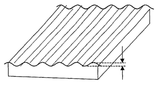
Figure 1 is a schematic of a typical grating showing the corresponding
diffraction pattern arising from such a grating;
Figure 2a is a schematic of sensing element having a sinusoidal surface;
io Figure 2b is the corresponding diffraction pattern obtained when analytes
bind to analyte-specific receptors coated on the sinusoidal surface of Figure
2a ;
Figure 2c shows the rippled surface covered with analyte-specific
receptors in contact with a medium of matching refractive index; so that the
interface is essentially invisible, when binding of analyte to analyte-
sepcific
is receptor occurs, there is a change of refractive index at the interface,
which
causes it to diffract light;
Figure 3a is a surface prepared with a PRIOR ART pattern of evenly
spaced lines of antibody (a 'biograting');
Figure 3b is a surface prepared with a pattern made using a 6-beam
2o splitter diffractive optic;
Figures 4a and 4b are the diffraction images obtained upon binding to the
patterned antibodies in Figures 3a and 3b, respectively, the scales are the
same
on both Figures 4a and 4b;
Figure 5a shows a diagrammatic illustration of an apparatus for performing
2s an assay in accordance with the present invention using a transmission
configuration;
Figure 5b shows a diagrammatic illustration of an apparatus for performing
an assay using a reflection configuration;
Figure 6a is a perspective view of a cell for performing an assay in the
3o static mode;
11
CA 02460233 2004-03-10
WO 03/023400 PCT/CA02/01395
Figure 6b is a cross-sectional view showing an embodiment of a flow cell
constructed for performing the present assay;
Figure 6c is a perspective view of an alternative embodiment of a flow cell
constructed in accordance with the present invention; and
Figure 6d is a cross-sectional view of a flow cell using total internal
reflection.
DETAILED DESCRIPTION OF THE INVENTION
The present invention provides a method for the assay of analytes using
to the principles of light diffraction from a patterned substrate. As
mentioned in the
background, the prior art has shown the feasibility of using the diffraction
of
incident light to indicatenthe presence of a specific type of analyte. The
present
invention provides a diffraction-based assay that is capable of high
sensitivity by
utilizing patterns on the substrate that are chosen to enhance the diffraction
is signal relative to those normally achieved with diffraction patterns using
evenly-
spaced parallel lines, which constitutes diffraction gratings.
In order to carry out an assay based on diffraction, recognition elements
are laid out on a substrate to define a pattern. In a preferred form, this
patterned
substrate is non-diffracting. The binding of analytes complementary to these
2o recognition elements will alter the local index of refraction and/or
topography
such that, upon illumination, the incident light is diffracted. Detection of
such
diffracted light indicates the occurrence of a binding event between analyte
and
receptor, and hence the presence of the analyte in the original medium being
assayed. In another embodiment, the initial substrate itself diffracts light.
In this
2s case, the binding event will still alter the local index of refraction
and/or
topography, and the intensity of the diffracted signal will change. For ease
of
signal detection, a preferred apparatus for this case is one that involves
filtering
such that this initial signal is nulled, using either optics or using
software.
It is well known in the field of optics that there is a correspondence
so between a given pattern and the pattern of light that is diffracted from
it. This
principle has not been utilized to the fullest in assays, and is the subject
of the
12
CA 02460233 2004-03-10
WO 03/023400 PCT/CA02/01395
present invention. The most common pattern used in diffraction studies is that
of
evenly spaced lines (a 'grating'), shown in Figure 1, and United States
Patents
Nos. 4,647,544 and 4,876,208 are based on such. The diffraction pattern that
arises from a grating is a series of evenly spaced bright dots ('Bragg peaks')
with
s diminishing light intensity as one moves away from the central beam of
light. The
spacing of the Bragg peaks is determined by the spacing of the lines in the
grating. In any assay, it is important to maximize the signal-to-noise ratio
in order
to increase sensitivity. In a diffraction-based assay using the example of the
grating shown in Figure 1, there typically is noise due to scattering of the
main
to beam, which can be large compared with the diffracted signal because of the
high intensity of the main beam which can swamp or wash out the typically
small
changes brought about by the binding events. One can try to reduce the noise
from the main beam and from stray scattering by detecting the diffracted
signal
as far away from the main beam as possible; however, the diffracted signal
also
is rapidly diminishes far from the main beam as mentioned above. Thus the
sensitivity and applicability of diffraction-based assays using a grating such
as
shown in Figure 1 is limited.
The present invention provides methods and devices for enhancing
signals obtained in a diffraction-based assay, together with the ability to
2o manipulate chemistry at a surface. The main concept is based on the
principle
that the pattern of recognition elements, which gives rise to the diffraction
of the
incident light in a diffraction-based assay, can be chosen in such a way so as
to
facilitate detection, and to enhance the signal to be detected. The pattern of
receptor molecules on the substrate may thus be made quite complex in order to
2s enhance signal and simplify detection. The detailed requirements may vary
depending on the specific application and constraints. There are three
different
methodologies and sensing elements that are disclosed herein to achieve this
result.
i) Sensing .Element Substrate With Selected Surface Topography
3o One embodimerit of the present invention comprises a substrate to which
the pattern recognition elements are bound which has a surface topography
13
CA 02460233 2004-03-10
WO 03/023400 PCT/CA02/01395
selected to give a diffraction image characterized by one or more diffraction
spots
spaced from the main light beam which are more intense than the spots obtained
using standard diffraction gratings. One example is a pattern that gives rise
to
only one diffracted spot, so that most of the diffracted intensity is
localized at this
s spot, and which is located as far away from the incident beam as possible,
so
that scattering due to the main beam is minimized. A surface having a
sinusoidal
function sin(kx) (or cosine(kx)) as shown in Figure 2a will yield exactly one
element in the Fourier transformation, located at +k as shown in Figure 2b. To
make k as large as possible (that is, the diffracted light be as far removed
from
to the incident beam), the period of the sine or cosirie should be about half
the
wavelength of the illumination. The analyte-specific receptors cover the whole
substrate so that the patterned recognition element is a composite of the
rippled
substrate plus the analyte-specific receptors covering the surface. The assay
is
preferably performed in contact with a solution the refractive index of which
is matches closely that of the patterned substrate, such that the interface is
essentially invisible, and none or very little light is diffracted prior to
binding. In
other words the reason index matching is preferred with this type of substrate
is
that the large signal a topography can generate will overwhelm the change due
to binding. In the case of a flat surface, there is no such signal diffraction
signal
20 ~ present so index matching is not required and one can use total internal
reflection.
The binding event highlights the rippled substrate by destroying the index
matching, and gives rise to the lone diffraction spot, see Figure 2b. It will
be
understood that the use of cosine (sine) surface topographies are only
illustrative
2s and a topography other than sinusoidal may be preferable.
For example, a topographical grating comprising evenly spaced lines but
which have larger topography than the analyte receptors can be used and the
analyte receptors are immobilized to cover the entire substrate, is one
possibility.
The substrate with the topographical grating and the medium are index matched
3o initially, so that no diffraction is observed. The binding of analytes in
the medium
14
CA 02460233 2004-03-10
WO 03/023400 PCT/CA02/01395
with the analyte specific receptors breaks the index matching, thus
highlighting
the grating, and resulting in a diffraction signal.
While the above examples illustrate sensor substrates having surface
topographical features that are much larger in scale than the analyte specific
s receptors, it will be understood that the sensor elements may be constructed
with
molecular scale topographical features, for example the sensor element could
include templated grooves the size of a large molecule having a complementary
geometry and interaction to the analytes. In other words, the analyte specific
receptors may comprise molecular to microscopic size indentations that would
~o provide complementary shape and interaction to specific proteins or cells,
which
are the analytes being tested for.
ii) Patterned Flat Substrates
The sensing element for the assay may be a solid substrate having laid
out on its planar surface a set of recognition elements or analyte-specific
is receptors in a pattern, either directly or through an intervening layer.
The pattern
is chosen to satisfy whatever criteria are desired for a specific assay, be it
the
enhancement of resolution, or simply for artistic purposes. In an assay for
multiple analytes on the same region, it may be desirable to use choose
surface
patterns for each analyte that will give rise to as different a diffraction
image as
2o possible, or at least contain regions of high diffracted signal intensity
that do not
overlap with those for other analytes.. In other words the entire diffraction
image
may not necessarily need to be distinct for each analyte. All that is needed
is that
there is one region or spot of each analyte that is distinct from others (i.e.
well-
separated spatially). In one embodiment of this invention, the pattern of
receptors
'2s on the substrate is chosen in such a way as to enhance the intensity of
the
diffracted signal away from the main beam, and reduce the intensity at the
main
beam as much as possible. The diffracted signal is preferably concentrated in
as~
few locations as possible.
3o iii) Diffractive Optic Elements
CA 02460233 2004-03-10
WO 03/023400 PCT/CA02/01395
Another class of pattern of interest is that~corresponding to optical
elements that steer light using the principles of diffraction, typically
resulting in
predetermined distinct patterns (diffractive optical elements). Most optical
elements manipulate light using the principles of reflection or refraction.
s Diffractive optic elements manipulate light by using the principles of
diffraction:
portions of the wavefront are retarded selectively using patterns on a
'substrate
typically glass, but other materials may be used as well. Diffraction permits
a
more versatile and powerful means of steering light. The patterns may be
surface
patterns formed on the surface of the element, or bulk patterns formed through
to the bulk of the material. Diffractive optic elements may have quite
complicated
patterns, but their versatility in manipulating light is useful in the current
bbjective
of optimizing properties of the diffraction image; a complicated pattern on
the
substrate is thus preferred compared with the prior art patterns of evenly
spaced
lines or circles.
is Diffractive optic elements are commercially available, or can be
manufactured to specifications, and common examples are attachments to laser
pointers that produce patterns such as a French cross, star, circles and the
like.
In this invention we are interested in difFractive optical elements that
diffract light
because of their surface topographical pattern. This type of diffractive
optical
2o element is useful in this invention in either of two ways: (1 ) the probe
molecules
are immobilized to cover the whole surface of the element, which is then
brought
into contact with the medium to be assayed as described in (i) above. The
refractive index of the medium is preferably matched or close to that of the
optical element; (2) The diffractive optical element is used as a master for
2s microcontact printing such that an elastomeric stamp is made from its
surface
topography. The probe molecule is thus patterned onto a substrate using this
elastomeric stamp according to the principles of microcontact printing and the
substrate is utilized as in (ii) above.
When being used, since the diffractive optic itself will have a~large
3o diffraction signal itself unless the medium is index matched so it is a
difference
or change in intensity that is monitored once the element is immersed in the
16
CA 02460233 2004-03-10
WO 03/023400 PCT/CA02/01395
medium. Intensity measurements may be made before exposure to the medium
containing the analytes in order to get a baseline or calibration which may be
stored in the processor. The presence of diffraction spots representative of .
binding of the analyte to the analyte-specific receptors is indicated by a
change in
s intensity of the measured diffraction signal.
A specific type of substrate that may be used in the diffraction-based
assay of the present invention is a diffractive optic beam splitter, which is
an
element that produces a preset number of beams of approximately equal
intensities from one incident beam. If this type of pattern is employed in a
io diffraction-based assay, the binding event will give rise to a
comparatively large
. diffracted signal, which is desirable in detection enhancement.
Complex patterns on a flat surface 'may be created by a variety of means.
Photolithography can be employed in many ways: light can be used to initiate a
reaction to activate or deactivate surface species, and by the appropriate
is application of masks, patterns can be formed. Printing techniques, such as
microcontact printing, inkjet printing and robotic spotting enables the
deposition
of material in desired patterns. The deposited material is either held,to the
substrate by physical adsorption, or can be covalently bound to the surface or
a
surface layer deposited on the substrate for the specific purpose of binding
to the
2o pattern recognition species. ,
For example, in addition to.using a diffractive optic element itself as a
substrate for recognition elements, a highly preferred patterned substrate may
be
prepared by microcontact printing using a diffractive optic element as a
master
and trarisferring the pattern from the diffractive optic element to a smooth
flat
2s substrate surface, such as for example glass, polymer, ceramic,
semiconductor
or metal, with or without additional coatings. Diffractive optic elements have
topographical patterns that are much more complicated than a grating of evenly
spaced lines. However, they can. easily be used as a mold to form an
elastomeric
stamp for use in microcontact printing. The pattern printed in this manner
will not
so be an exact replica of the diffractive optic element since only the spacing
between topographic features will be reproduced, but not the depth of the
17
CA 02460233 2004-03-10
WO 03/023400 PCT/CA02/01395
grooves. However, the diffraction signal will be much enhanced over that
produced by an ordinary grating comprising straight parallel grating lines.
The assay is performed by contacting the patterned substrate with the
analyte-containing medium. The solid substrate upon which the pattern of
recognition elements is laid may be transparent, partially transparent, or
reflecting at the wavelength of the incident illumination. In the case of a
transparent substrate, analyte-specific receptors may be patterned on one or
both surfaces of the substrate. Once the recognition element that is capable
of
specific binding (e.g., protein, .oligonucleotide, antibody, etc.) is laid out
on the
to surface in a preselected pattern, the medium to be assayed is contacted
with the
substrate, allowing analytes present in the medium to bind to their
complementary recognition element.
When a particular analyte is present in the medium, the subsequent
binding event between analyte and its complementary recognition element is
is accompanied by a change in the local thickness of the layer on the
substrate
and/or in the local index of refraction. Both the change in thickness and the
change in index of refraction will alter the optical properties at the
interface
between the substrate and medium in regions where the binding has taken place.
Since the recognition elements are present on the substrate in a predetermined
2o pattern, light incident on the substrate will not be scattered uniformly,
but rather
will be diffracted. In one embodiment of this invention, the patterned
substrate is
non-diffracting, and the binding events result in an observable diffraction
image.
In another embodiment, the patterned substrate itself produces an observable
diffraction image, but the binding events alter the intensities of the
diffracted
2s ' signal.
The diffracted signal strength may be enhanced by the addition of one or
more secondary species selected to localize on the already immobilized
analytes. The secondary species may contain a substance that will enhance the
change in index of refraction (such as a chromophore, a metal colloid with a
3o plasmon band, resonant with the source wavelength, or an enzyme that can
cause a precipitate to form when appropriate reagents are added), or enhance
18
CA 02460233 2004-03-10
WO 03/023400 PCT/CA02/01395
the change in height above the substrate (such as a large particle, a metal
colloid, a polymer colloid, a quantum dot, a protein), or both.
Alternatively, the analytes may be pre-treated so as to be first coupled to a
material that will enhance the signal obtained upon binding, either through a
s change in refractive index, or in height, or both. This material may be a
polymer
colloid, a large molecule, a chromophore or a metal colloid. The chromophore
or
metal colloid should preferably absorb radiation at the wavelength of the
source
illumination.
In one embodiment of the invention, after the substrate surface has been
to exposed to the medium being screened for the analytes, the substrate is
rinsed
and dried prior to the diffraction measurement. In another embodiment, the
assay
is performed in situ with the substrate immersed in the solution containing
the
analyte. This is the preferred mode when index matching is desired to enhance
the diffraction signals as discussed above with respect to the substrates with
the
is modified surface topography. In this case, the kinetics of the binding
event may
be examined by monitoring the evolution of the diffraction signal. The assay
is
made quantitative by a measurement of the intensities at selected regions of
the
diffraction signal, and by the use of predetermined calibration standards or
alternatively by fitting to known binding kinetics.
2o The assay has been described for a single type of analyte. The present
method includes extension to detecting multiple analytes in a medium and
involves producing multiple patterns of recognition elements within the same
substrate. The pattern for each type of recognition element may either be
distinct
from that of others, or they may be the same, but simply located in different
2s regions of the.substrate. The following are non-limiting examples of simple
distinct patterns: (1 ) They~may consist of different geometric elements
(lines,
circles, etc.) (2) They may be of the same geometric elements but arrangedwith
different periodicities. (3) They may be of the same geometric elements with
the
same periodicity but rotated with respect to each other, provided the patterns
do
3o not have rotational symmetry. (4) They may be a mixture of any of the
above. In
the case of multiple patterns of multiple recognition elements, it is
desirable to
19
CA 02460233 2004-03-10
WO 03/023400 PCT/CA02/01395
have regions of high intensity such that at least one region is distinct to
each
pattern employed. In other words the diffraction patterns may overlap but at
each
pattern should have at least one unique spot.
In applications in which moisture may be problematic, the substrate may
s be placed in a cell that is partially evacuated in order to reduce moisture.
This is
advantageous where it is desirable to reduce the signal strength that may
arise
due to water condensation. However, in the case where the analytes but not
their
partner receptors are favoured by water, the presence of water condensation
(also called 'condensation figures') can be utilized to enhance the diffracted
to signal.
In another embodiment of the invention, the assay may also be performed
in situ by placing the substrate into a chamber into which the medium can be
introduced. Figure 6a shows a cell 50 with a substrate 52 immersed in a liquid
being tested for the presence of one or more of the analytes in a static
is configuration with no flow-through. Analyte-specific receptors are
patterned on
one or both surfaces of substrate 52.
Figure 6b shows a flow configuration comprising a cell 56 comprising
spaced parallel walls 58 and 60 with analyte-specific receptor patterns formed
on
the insides of each of the walls. The liquid is continuously flowed through
the cell
2o during operation and the reflection or transmission mode may be used as
indicated by the arrows. Figure 6c shows another embodiment of a flow cell 66
comprising spaced parallel walls 68 and 70 with wall 70 having an inlet port
72
and an outlet port 74. The analyte specific receptor pattern 76 is formed on
the
inner surface of wall 68, and an O-ring 78 is used to seal the flow chamber.
In
2s each of these embodiments the chamber should have at least one window
transparent to the incident illumination. The substrate within the chamber is
located in direct line of illumination, and the assay is performed either in
reflection or transmission, as described previously. In another embodiment,
the
fluid chamber may comprise the patterned substrate as one or more of its
3o windows. In these embodiments, the time dependence of the binding events
may
be monitored simultaneously for all analytes. This may be useful for
'20
CA 02460233 2004-03-10
WO 03/023400 PCT/CA02/01395
measurement ofi relative binding affinities.
In certain cases, as will be described in the examples hereinafter, the
diffracted signal will be strong enough to be visible to the unaided eye under
proper lighting conditions. In this case, all that is needed is the observer's
eye, or
s for a more permanent record, any camera, or similar imaging device. For
quantification of low intensity signals,.a sensitive CCD array detector or a
PMT
may be used. For further signal enhancement, lock-in detection as well as
amplification schemes known to~those skilled in the art may be employed. As
discussed previously, the image, or a part thereof, obtained as an electronic
~o signal from the detector is stored an a computer and image analysis
software is
then used to identify the patterns on the substrate that gave rise to the
observed
diffraction image thus identifying which analytes are present in the medium. A
code may be written on the substrate itselfi that identifies which analyte-
specific
receptors are present. The presence of signals at specific locations relative
to a
~ls standard encoded location within the diffraction image corresponds to the
presence of specific analytes. Quantification of signals at defiined locations
enables quantification of the amount of different analytes.
In operation, the recognition elements that are capable of specific binding
(e.g., protein, oligonucleotide, antibody, etc.) are laid out on a surface in
2o preselected patterns. The medium to be assayed is contacted with the
substrate,
allowing analytes present in the medium to bind to their complementary
recognition ,element. It should be noted that the recognition element could be
a
structural or topographical feature such as grooves formed in the top surface
of
the substrate having dimensions and/or interactions to trap the target ofi
interest
2s such as a bacterium. In one embodiment of this invention, the substrate is
rinsed
and dried, and placed in one of the devices previously described such that the
substrate with the bound analytes is placed in direct line of the light beam
from
the light source 32. The substrate may be a dipstick.
While it is simplest to utilize a clear medium, such as an aqueous solution,
~3o this method can also be used for assay of analytes present in other media.
The
medium may generally be a filuid including gas or liquid and the analytes can
21
CA 02460233 2004-03-10
WO 03/023400 PCT/CA02/01395
include various biological pathogens, environmental toxins or chemical warfare
agents dispersed in air. In one embodiment of this invention, analytes present
in
complex media such as urine, blood, serum, plasma or other turbid media are
assayed. If the medium is not completely transparent to the incident
illumination,
the assay is best performed under reflection configuration. The assay of
analytes
in complex media may be complicated by degradation of signal-to-noise due to
scattering and/or absorption of the incident illumination by the medium. Thus,
in
one embodiment of the invention the apparatus used to perform the assay uses
total internal reflection of the incident light from the substrate-medium
interface.
io Referring to Figure 6d, a substrate 84 having analyte-specific receptor
patterns
86 is in contact on one side thereof with the medium 82 being tested, which is
contained within a chamber 80. Light is totally reflected from the interface
between substrate 84 and medium 82. The cell operates as a flow cell when
fluid
is pumped through tube 90 into chamber 80 and out of tube 92. In another
Is embodiment of this invention, the incident illumination is chosen so that
the
complex medium is transparent at the wavelength of the light, for example, the
use of near-infrared laser wavelengths for the assay of fluids such as blood
and
the like.
Referring to Figures 5a~ 5b and 5c, detector 34 must be sensitive to the
2o illumination of choice. The detector 34 may be a position sensitive
photodiode, a
photomultiplier tube (PMT), a photodiode (PD), an avalanche photodiode (APD),
a charged-coupled device (CCD) or a CMOS array, the unaided eye, a camera, a
photographic plate, or any other imaging device. In one embodiment of this
invention, the transmitted or reflected signal is collected by an imaging
optical
as fibre and directed to an imaging detector. Detector 34, is attached to the
appropriate accessories to provide power and enable signal collection and data
processing. If a position sensitive photodiode is used it is first calibrated;
the
intensity of the signal reflects the position of the pattern impinging on the
detector.
so The photodiode, photomultiplier tube or avalanche photodiode is mounted
on a translation stage. By moving the detector on the stage, the pattern of
high
22
CA 02460233 2004-03-10
WO 03/023400 PCT/CA02/01395
and low light levels are mapped out. Alternatively, the PMT, or (APD) may be
held
in a stationary position. A mirror is positioned to direct the light from the
substrate
to the PMT, PD or APD. This mirror is mounted on a rotation stage, and by.
rotating the stage, the pattern of low and high light levels can be mapped out
on
s the PMT, I?D or APD as shown in Figure 5c.
When a CCD array or other imaging device is used, it is positioned to
collect either the full diffraction image, or a part thereof. In the latter
case, the
imaging device is mounted on a translation stage to enable inspection of
selected
regions of the diffraction image; changes in the intensities signify the
binding
to event(s). The following non-limiting examples are intended to further
illustrate the
invention.
Example 1
Preparation of Patterned Substrate By Microcontact Printing
The substrates were patterned by microcontact printing essentialy
following the procedure described in Bernard, A; Delamarche, E.; Schmid, H.;
Michel, B.; Bosshard, H.R.; Biebuyck, H.; "Printing Patterns Of Proteins"
Langmuir (1998), 14, 2225-2229. For evenly-spaced masters (diffraction
grating),
2o electron microscope grids or masters prepared by standard photolithography
were used; otherwise various diffractive optics (Thor Labs) were employed. The
poly(dimethylsiloxane) (PDMS) stamps were fabricated by using typically 10%
crosslinking (Sylgard 184 Silicone elastomer kit, Dow Corning Corporation
purchased from Paisley Products, Ontario Canada) and curing at 50-60° C
for
2s 14-18 h. The PDMS stamps prepared in this manner have a diffractive surface
of
~50 mm2. The PDMS stamp was cleaned by sonication in a 2:1 solution of
distilled and deionized water (ddH20)/ethanol for 5-10 min, followed by drying
under a stream of nitrogen gas (N2) and applying a fresh piece of adhesive
tape
to the stamp surface. The tape was removed from the stamp surface after a few
minutes, 150-200 uL of protein at 50-100 ug/mL in phosphate buffered saline
(PBS) was immediately applied to the stamp surface and allowed to stand at
room temperature. After 30 min, the solution of protein was removed and the
23
CA 02460233 2004-03-10
WO 03/023400 PCT/CA02/01395
inked stamp surface was washed with PBS (2x2mL), ddH20 (2x2mL) and, finally,
dried under a stream of N2. The stamp was then applied under light pressure to
a
substrate, previously cleaned by sonication in 2:1.ddH~O/EtOH and dried under
a
stream of N~, and left in place for several seconds. The stamped substrate was
s then washed with PBS (2mL), ddH20 (2mL) and dried under a stream of N2. A
substrate prepared in this manner is shown in Figure 4, where the deposited
material is visualized using atomic force microscopy.
If subsequent patterns were desired on the same substrate, they were
produced by using additional PDMS stamps cleaned, inked and stamped in the
1o same manner as above, but cross-stamped onto the substrate at angles offset
from the existing patterns.
Example 2
Signal Measurement
is The substrate was illuminated with either a Nd:YV04 laser (lambda = 532
nm) or a red diode laser (lambda = 650 nm). The diffraction image of crossed-
stamped substrates resulting from illumination by either laser can be visually
observed in transmission or reflection mode prior to addition of analyte. For
visual and photographic signal detection, the intensity of the diffracted
light was
ao reduced to the point when the diffraction image was no longer discernible
by eye
using a neutral density filter before the addition of analyte. For electronic
signal
detection, the intensity was reduced with a neutral density filter to.a small,
but
measurable value to maximize the signal range of the detection device before
the
addition of analyte.
2s
Example 3
"Dry" Measurement
In the "dry" measurement scheme, the substrate was immersed in a
solution containing the analyte for the specified period of time. The
substrate
3o was then removed from the analyte solution, washed with PBS (2 mL) and
ddH20 (2mL), and dried under a stream of N2. The substrate was illuminated
with
24
CA 02460233 2004-03-10
WO 03/023400 PCT/CA02/01395
a laser and a visible diffraction image could be discerned by eye and the
intensity
measured using a CCD linear array or CCD area array detector hooked up to a
computer. Alternatively, a photomultiplier tube mounted on an x-y translation
stage was used to measure the signal intensity of a specific spot on the
diffraction image by moving it across the spot while recording the intensity
on an
oscilloscope.
Example 4
Goat IgG Patterned Substrate Tested with Anti-goat Gold Conjugates
to Goat IgG was patterned as described above onto two glass substrates
using a grating and a six-beam splitter diffractive optic, respectively.
Figures 3a
and 3b are images of these substrates visualized using atomic force
microscopy.
The resulting patterned substrates were immersed in anti-goat IgG gold
conjugate solution for 30-60 min and then removed and washed with PBS
is (2x2m1) and ddH20 (2x2m1) and dried under a stream of N~. The development
of
the diffraction images observed in both the transmitted and reflected modes
corresponding to goat IgG on the substrate was monitored visually and recorded
using a CCD camera; image analysis software was utilized to make a
comparison of the intensities of the diffracted signal. The results are
summarized
2o in Figures 4a and 4b. The patterned substrate prepared from a diffractive
optic
beam splitter as master showed strong diffraction signals away from the centre
(main beam), while the substrate prepared using the prior art parallel line
grating
showed a rapid decay in signal.
As used herein, the terms ''comprises", ".comprising", "includes" and
2s "including" are to be construed as being inclusive and open ended, and not
exclusive. Specifically, when used in this specification including claims, the
terms
"comprises" and "comprising" and variations thereof mean the specified
features,
steps or components are included. These terms are not to be interpreted to
exclude the presence of other features, steps or components.
3o The foregoing description of the preferred embodiments of the invention
has been presented to illustrate the principles of the invention and not to
limit the
CA 02460233 2004-03-10
WO 03/023400 PCT/CA02/01395
invention to the particular embodiment illustrated. It is intended that the
scope of
the invention be defined by all of the embodiments encompassed within the
following claims and their equivalents.
26