Note: Descriptions are shown in the official language in which they were submitted.
CA 02460765 2004-03-12
MEMS OPTICAL LATCHING SWITCH
[0001] This application claims the benefit of Provisional Patent Application
No.
60/456,063, filed 03/19/2003.
BACKGROUND
[0002] This invention in embodiments relates to microelectromechanical
system (MEMS) switches and more particularly to multiple state optical
latching
switches.
[0003] The telecommunications industry is undergoing dramatic changes with
increased competition, relentless bandwidth demand, and a migration toward a
more
data-centric network architecture. First generation point-to-point wave
division
multiplex systems have eased the traffic bottleneck in the backbone portion of
a
network. As a new cross-connect architecture moves the technology closer to
the
subscriber side of the network, operators are challenged to provide services
at the
optical layer, calling for more flexible networks that can switch and reroute
wavelengths. This is placing great emphasis and demand for wavelength agile
devices.
[0004] The need to provide services "just in time" by allocation of
wavelengths,
and further migration of the optical layer from the high-capacity backbone
portion to
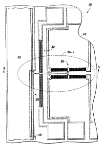
the local loop, is driving the transformation of the network toward an all
optical
network in which basic network requirements will be performed in the optical
layer.
[0005] The optical network is a natural evolution of point-to-point dense
wavelength division multiplexing (DWDM) transport to a more dynamic, flexible,
and
intelligent networking architecture to improve service delivery time. The main
element
of the optical network is the wavelength (channel), which will be provisioned,
-1-
CA 02460765 2004-03-12
configured, routed, and managed in the optical domain. Intelligent optical
networking
will be first deployed as an "opaque" network in which periodic optical-
electrical
conversion will be required to monitor and isolate signal impairments. Longer
range,
the optical network will evolve to a "transparent" optical network in which a
signal is
transported from its source to a destination totally within the optical
domain.
[0006] A key element of the emerging optical network is an optical add/drop
multiplexer (OADM). An OADM will drop or add specific wavelength channels
without
affecting the through channels. Fixed OADMs can simplify the network and
readily
allow cost-effective DWDM migration from simple point-to-point topologies to
fixed
multi-point configurations. True dynamic OADM, in which reconfiguration is
done in
the optical domain without optical-electrical conversion, would allow
dynamically
reconfigurable, multi-point DWDM optical networks. This dynamically
reconfigurable
multi-point architecture is slated to be the next major phase in network
evolution, with
true OADM an enabling network element for this architecture.
[0007] On chip integration of optical switching and planar light circuits has
the
potential to greatly reduce the size and manufacturing costs of multi-
component
optical equipment such as Reconfigurable Optical Add/Drop Multiplexers
(ROADMs).
Current costs for Reconfigurable Optical Add/Drop Multiplexers (ROADMs) are
$1,000 per channel, limiting their use to long-haul optical telecommunications
networks. In order to extend their use into the metropolitan network the cost
will
need to be decreased by an order of magnitude to $100 per channel, without
sacrificing performance.
[0008] One solution to decreasing cost is through the integration of
components, where the primary cost savings will be in packaging. A number of
approaches are being pursued for optical integration using Planar Light
Circuit (PLC)
technologies. The majority of approaches use a silica-on-silicon platform with
the
ROADM formed from the integration of silica Arrayed Waveguide Gratings (AWG's)
for multiplexing and demultiplexing, with Thermo-Optic (TO) switches for
performing
-2-
CA 02460765 2004-03-12
the add/drop and pass of the demultiplexed signal. The use of a low-index
contrast
silica-on-silicon platform severely limits the yield of these components due
to the
requirement for uniform thick oxide films over large areas to form the
waveguides.
The use of TO switches limits the extensibility due to high-power requirements
and
thermal cross-talk.
[0009] A number of different materials and switching technologies are being
explored for fabricating chip-scale photonic lightwave circuits such as AWG's
for
demultiplexers and multiplexers, Variable Optical Attenuators (VOA's) and
Reconfigurable Optical Add-Drop Multiplexers (ROADMs). The main material
platforms include silica wafers, silica-on-silicon substrates using both thin
film
deposition and wafer bonding techniques, polymer waveguides defined on silicon
substrates, and silicon-on-insulator substrates. The main switching
technologies
include Mach-Zehnder interferometers based on either a thermo-optic or electro-
optic
effect, and MEMS mechanical waveguide switches.
[0010] While silica waveguides have optical properties that are well matched
to
the optical properties of conventional single mode fibers, and thus couple
well to
them, they require thick cladding layers due to the low index of refraction
contrast
between the waveguide core and cladding materials, making them difficult to
fabricate using planar processing techniques for fabrication and integration
with other
on-chip optical devices. The low index of refraction contrast, Vin, between
core and
cladding also requires large bending radii to limit optical loss during
propagation
through the photonic lightwave circuit, leading to large chip footprints and
low die
yields (<50%).
[0011] In addition, silica based waveguide switches are typically based on
Mach-Zehnder interference using thermo-optic effects, that have a limited
Extinction
Ratio (ER) of around 25-30 dB, require significant power due to the low thermo-
optic
coefficient of silica, have problems with thermal cross-talk between the
different
-3-
CA 02460765 2004-03-12
optical channels and have a sinusoidal rather than a digital optical response.
They
also lose their switching state when power is lost.
[0012] What is needed is a Silicon-On-Insulator (S01) platform for
monolithically integrating optical, mechanical and electrical functions. The
use of a
silicon platform enables fabrication of components using the vast
infrastructure and
process development available for semiconductor iC manufacturing at silicon
foundries. By fabricating the MEMS switches and waveguides in the same
material,
single crystal silicon, there are no stress and strain issues as exist with
heterogeneous materials sets such as silica-on-silicon. Fabrication in silicon
also
allows for integration with CMOS microelectronics for control and sensing
capabilities, and for free-carrier plasma dispersion effects to enable signal
leveling
using integrated VOA's. The high index contrast of silicon (n = 3.5) enables
the ridge
waveguide structures to make tight turns with minimum optical bending loss,
decreasing overall chip size to centimeter dimensions.
-4-
CA 02460765 2004-03-12
SUMMARY
[0013] An optical micro-electro-mechanical system (MEMS) switch is
disclosed. In a preferred embodiment the optical MEMS switch is used as an M x
N
optical signal switching system. The optical MEMS switch comprises a plurality
of
optical waveguides formed on a flexible cantilever beam platform for switching
optical
states wherein the state of the optical switch is changed by a system of drive
and
latch actuators. The optical MEMS device utilizes a latching mechanism in
association with a thermal drive actuator for aligning the cantilever beam
platform. In
use the optical MEMS device may be integrated with other optical components to
form planar light circuits (PLCs). When switches and PLCs are integrated
together
on a silicon chip, compact higher functionality devices, such as
Reconfigurable
Optical Add-Drop Multiplexers (ROADMs), may be fabricated.
BRIEF DESCRIPTION OF THE DRAWINGS
[0014] The drawings are not to scale and are only for purposes of
illustration.
[0015] FIG. 1 is a cut away top plane view of an optical MEMS (Micro Electro
Mechanical System) switch in accordance with the present invention;
[0016] FIG. 2 is an enlarged view of a portion of FIG. 1 for illustrative
purposes;
[0017] FIG. 3 is a side cross-sectional view of FIG. 2;
[0018] FIG. 4 is a graphically view of a timing diagram for controlling a
latch
and drive switch shown in FIGS. 1 and 2;
[0019] FIG. 5 is a top plane view showing the latch actuated to an open
position;
[0020] FIG. 6 is a top plane view showing the drive switch actuated to an
overshoot position;
-5-
CA 02460765 2004-03-12
[0021 j FIG. 7 is a top plane view showing the latching mechanism in the
latched position;
[0022] FIG. 8 is a cut away top plane view of an optical MEMS device with a
"hook" hitch and latch teeth in accordance with another embodiment of the
present
invention;
[0023] FIG. 9A is an enlarged view of a portion of FIG. 8 detailing the "hook"
hitch in an equilibrium state;
[0024] FIG. 9B is an enlarged view of a portion of FIG. 8 detailing the latch
teeth in an equilibrium state;
[0025] FIG. 10A is an enlarged view of a portion of FIG. 8 detailing the
"hook"
hitch in a first switch state;
[0026] FIG. 10B is an enlarged view of a portion of FIG. 8 detailing the latch
teeth in a first switch state;
[0027] FIG. 11A is an enlarged view of a portion of FIG. 8 detailing the
"hook"
hitch in a second switch state; and
[0028] FIG. 11 B is an enlarged view of a portion of FIG. 8 detailing the
latch
teeth in a second switch state.
DETAILED DESCRIPTION
[0029] Referring now to FIG. 1 there is shown a top plane view of an optical
MEMS (Micro Electro Mechanical System) switch 10. All optical and moving
mechanical components shown are fabricated in the single-crystal silicon
device
layer of a SOI wafer using a self-aligned process. The optical MEMS switch 10
utilizes a latching mechanism 20 in association with a thermal drive actuator
30 for
aligning a flexible cantilever beam platform 50 fixed at one end 58. The
flexible
-6-
CA 02460765 2004-03-12
cantilever beam defines one or more movable waveguides for switching to one or
more stationary waveguides defined on an optical slab 40. The components
fabricated in the device layer of an SOI wafer may be released by sacrificial
etching
of the buried oxide layer. In use the optical MEMS switch 10 may be integrated
with
planar light circuits (PLCs). When switches and PLCs are integrated together
on a
silicon chip higher functionality devices, such as Reconfigurable Optical Add-
Drop
Multiplexers (R-OADM), may be fabricated.
[0030] As shown in FIGS. 1 through 3, the optical switch 10 comprises one or
more thermal drive actuators 30 having associated during fabrication one or
more
thermal latch actuators 21, each thermal latch actuator 21 supports
translating latch
teeth 22. The flexible cantilever beam platform 50 defines a plurality of
optical
waveguides 52 and 54. A tether 34 connects the one or more thermal drive
actuators
30 to the flexible cantilever beam platform 50. A linkage 28 connects the
thermal
drive actuators 30 to a set of linkage teeth 24 wherein the linkage teeth 24
are
contacted by the latch teeth 22 when the latch is engaged. The linkage teeth
24 and
latch teeth 22 are spatially located to determine one or more latched state
positions
wherein electrical stimuli is timed to actuate the thermal drive 30 and
thermal latch
actuators 21 so as to switch between equilibrium and latched states as will be
more
fully described below.
[0031] The optical MEMS switch 10 is applicable as an optical switch in a
variety of applications, such as optical fiber transmission networks, to route
optical
signals along various signal paths. Switches are typically characterized by
the
number of input and output ports, referred to as MxN. For example, a 1 x3
switch
would switch one input between three outputs. MxN switches have previously
been
implemented using waveguide shuttles or by cascading a series of M 1 xN
cantilever
switches. While shuttle switches can provide the MxN switching functionality,
they
require at least two gaps in the optical pathway, which leads to increased
optical
losses. Similarly, a series of M cascaded cantilever switches would have M
optical
-7-
CA 02460765 2004-03-12
gaps which leads to increased optical losses for M>1. By fabricating an MxN
cantilever beam waveguide switch, where a cantilever beam carrying M
waveguides
is deflected rather than a waveguide shuttle, only one optical gap is required
in the
optical pathway, cutting the optical loss associated with propagation through
the gaps
in half. Alternatively M cantilever beams, each carrying a single waveguide,
can be
flexibly connected so that they all actuate together. Furthermore, reflections
from the
two gaps associated with a shuttle can cause additional losses due to
interference.
[0032] Turning once again to FIGS. 1 through 5 there is shown the optical
switch 10 with two optical waveguides 52 and 54 formed on the flexible
cantilever
beam platform 50 for switching between two stationary optical waveguides 42
and
44., respectively. This configuration enables two optical signals to be
switched at the
same time. By including additional optical waveguides, additional signals may
be
switched simultaneously. The ability to switch multiple signals at the same
time is
important in many optical applications. For example, in an R-OADM
(Reconfigurable
Optical Add/Drop Multiplexer), when an input signal is dropped, a new signal
can be
added to the output. Since the add/drop function always occurs simultaneously,
it is
possible to decrease the number of required optical switches by implementing a
single cantilever switch that performs the add drop function on both the input
signal,
sending it to the drop line, and the add signal, sending it to the switch's
output.
Referring to FIG. 3, the optical multiple state latching switch 10 uses oxide
anchors
56 to attach components to the substrate 60. As well known in the art,
polysilicon
anchors can be utilized instead of oxide. Polysilicon can also be used to
fabricate
dimples, as commonly practiced in MEMS to avoid stiction.
[0033) Referring now to FIG. 4 there is graphically illustrated the timing
sequence of the signals used to actuate the drive and latch mechanisms for the
2x2
switch illustrated in FIG. 1, where the voltages are labeled in FIG. 4
assuming the
potential of the handle wafer or base substrate 60 is zero. The first portion
of the
timing diagram shows the latching sequence. The first step in the latching
sequence
_g_
CA 02460765 2004-03-12
is to apply a voltage +V1 to one end 26 of each latch actuator 21, and a
voltage -V1
to the other end 45 of each latch actuator 21. The voltages on the latch
actuators
induce ohmic heating in the actuator beams, causing thermal expansion and the
subsequent opening (direction 27) of the latch as shown in FIG. 5. While the
latch
actuator voltage is still applied, the drive actuator 30 is stimulated with a
voltage + V2
at one end 31 and a voltage -V2 at the other end 33.
[0034] FIG. 6 shows how the resulting thermal expansion of the drive actuator
30 is sufficient to move the flexible cantilever beam platform 50 and linkage
28 far
enough to the right for the linkage teeth 24 to be well to the right side of
the latch
teeth 22. Next the latch actuator voltages return to zero, and the latch
closes. To
finish the latching sequence, the drive actuator voltages return to zero. As
the drive
actuator cools, the linkage teeth 24 are drawn in tension (direction 37)
against the
latch teeth 22 which holds the switch in the desired latched position as shown
in FIG.
7. To return the switch to its original state, the same sequence of voltages
are
applied in the reverse timing, as shown in the unlatch portion of FIG. 4.
Unlike
switches with no latching capability, the optical MEMS latching switch 10 only
consumes power during a change of state, and preserves its state, even if
power is
interrupted.
[0035] It should be noted that, although the timing diagram shown in FIG. 4
depicts square wave voltage pulses, this depiction is meant to be illustrative
only of
the basic timing, and does not preclude the use of other waveforms.
Furthermore,
the voltages applied to the thermal actuators need not be symmetric about
zero.
However, the use of equal but opposite polarity pulses, as described above,
results in
a constant zero voltage at the center of each actuator throughout the latch
and
unlatch cycle, which reduces electrostatic forces between the actuators and
the
handle wafer 60.
j0036] A logic table for the 2x2 switching function is as follows:
[0037] State One: AddIDrop function, as shown in FIG. 5
_g_
CA 02460765 2004-03-12
[0038] The left movable waveguide 52 (input) is optically aligned
to the left stationary waveguide 42 (drop).
[0039] The right movable waveguide 54 {add) is optically aligned
to the right stationary waveguide 44 (output).
[0040] State Two: Pass function, as shown in FIG. 7
[0041] The left movable waveguide 52 (input) is optically aligned
to the right stationary waveguide 44 (output).
[0042] In order to change from state one to state two, a force F can be
applied
by a thermal drive actuator 30. In order to deflect the free end by a distance
sx, a
force F must be applied where F is given by:
F = (Ea3b/4L3)8x
[0043] Where E is Young's modulus (E = 1.65 x 10⁵ ~.N/ ~m2 for single crystal
silicon), a is the thinner cross-sectional dimension of the beam 21, b is the
thicker
cross-sectional dimension of the beam and L is the length of the beam. For
example,
a 1000 ~m long beam that is 5~m thick and 20 ~m wide would require a force of
13.2
~N to deflect the free end by 8 ~,m, which is sufficient deflection to switch
a cantilever
beam with two 4 ~m waveguides.
[0044] The switching force F can be applied to the free end of the cantilever
beam 50, or at an intermediate location, or locations as required. The switch
can
also be actuated in the opposite direction by applying a force F from the
thermal drive
actuator 30 in the opposite direction. In some cases it may be preferable to
not use
the equilibrium position of the cantilever beam, since these do not have a
strong
restoring force that returns them to this position since the cantilever beam
may be
quite long and flexible. Instead only deflected positions may be desirable to
use. In
addition, it may be advantageous to angle the receiving waveguides to better
match
the direction of propagation of the light leaving the deflected cantilever
beam.
-10-
CA 02460765 2004-03-12
[0045] Since the cantilever beam carrying multiple waveguides could be wider
than it is thick, it could suffer undesirable out of plane deflections since.
it is less stiff
out of plane than it is in plane, as predicted by the formula
K = (Ea/4)(b/L)3
[0046) As an example for a beam that is 5 ~m thick and 20 ~m wide, the ratio
of the stiffness in the horizontal direction of the vertical direction is
(20/5)2. The beam
is 16 times stiffer in the horizontal direction relative to the vertical
direction.
[0047] In order to avoid out of plane deflections the appropriate location
along
the cantilever beam 50 may be attached to a switch tether 34 so as to minimize
these
out of plane deflections. The beam's width may also be decreased at certain
points to
decrease its stiffness in the horizontal direction (e.g. serrated). Joints can
be added
to make the beam more flexible in the horizontal direction. The beam can be
deflected bi-directionally to decrease the magnitude of the required
deflection. The
beam can be thickened or stiffened to make it less flexible in the out-of-
plane
direction (e.g. by making the beam thicker or by adding super structures such
as
additional beams).
[0048] The switches and the waveguides are made together on a single crystal
silicon wafer using widely available semiconductor processing equipment. Such
on-
chip integration avoids the complex alignment issues associated with manually
connecting different and larger components with optical fibers, and avoids the
cost
and space associated with manufacturing, assembling and packaging the separate
components of optical switches. On-chip integration with other components can
drive
down the cost of manufacturing switches and installation of these complicated
devices by a factor of ten or more. Currently, these components cost over
$1,000
per channel.
-11-
CA 02460765 2004-03-12
[0049] FIGS. 8 through 11 shows two extensions 100 of the system
embodiment depicted in FIG. 1. The first extension is to a higher order of
switching,
from 2x2 in FIG. 1 to 2x3 in FIG. 8. The second option shown in FIG. 9A is the
introduction of a "hook"-hitch 132 and 134 instead of a simple tether. These
two
extensions are discussed below.
[0050) To increase the system from a 2x2 switch to a 2x3 switch, two
additional elements are required. The first is another stationary waveguide
platform
defining stationary waveguides 142, 144 and 146 respectively. The second
element
is an extra pair of teeth 25 on the linkage 28 located after the teeth set 24
as shown
in FIG. 9B. For the initial state of the 2x3 switch, the latch teeth are
disengaged as
shown in FIG. 9B. In this position, the right most moveable waveguide 154 is
aligned
with the left most stationary waveguide 142 as shown in FIGS. 8 and 9A. Using
an
actuation sequence similar to the latching phase shown and described in FIG.
4, the
switch can be moved to a second state as shown in FIG. 10B. Here the latch
teeth
22 defined by the latch actuator 21 engage between the pair of teeth 24 and 25
on the
linkage 28, and the two movable waveguides 152 and 154 are align with the left
most
pair of stationary waveguides 142 and 144 respectively, as shown in FIG. 10A.
A
third state can be achieved by executing another latching sequence with higher
voltages on the drive. In this state, depicted in FIGS. 11A and 11B, the latch
teeth
22 engages behind the pair of linkage teeth 24 and the two moveable waveguides
152 and 154 now align with the right most pair of stationary waveguides 144
and
146.
(0051] The 2x3 switch example discussed above, is one embodiment of the
general ability to achieve NxM switching for small values of N and M. Each NxM
configuration requires a sufficient number of fixed and movable waveguides.
Further
design considerations may be accounted for to achieve the desired set of
switch
positions. These include the initial relative alignment and spacing of the
moveable
-12-
CA 02460765 2004-03-12
and stationary waveguides, as well as, the number and relative location of the
linkage teeth.
[0052] The second option shown in FIGS. 8 through 11 is the substitution of an
interlocking "hook" hitch 132 and 134 for the tether 34. Depending on the
embodiment and fabrication processes employed, the "hook" hitch may be used to
mitigate the affects of stresses that may degrade the switch performance. For
example, if the process were to induce stress in the drive actuator 30, the
stress
could be transferred through a tether 34, and impact the equilibrium state
alignment
of the waveguides. The "hook" hitch mechanically decouples the drive actuator
130
from the moveable waveguide platform 150 in the equilibrium state, thereby
eliminating any transferred stress that would induce a misalignment in the
equilibrium
state.
[0053] The "hook" hitch also mitigates stresses that occur in latched states
that lead to undesirable rotations in the linkage. As the unanchored end of
the
cantilevered waveguide platform is pulled to the right, the translational
motion of the
plattorm is accompanied by a small clockwise rotation due to the bending of
the
cantilevered platform. If a simple tether is used, the rotation of the
waveguide
platform bends the tether 34, which in turn causes a counter clockwise
rotation of the
linkage 28, and may also asymmetrically distort the drive actuator. The
rotation of
the linkage and asymmetric distortion of the actuator is most severe in
systems that
require larger displacements. The "hook" hitch, however, provides a good
counter
measure for these issues. As seen in FIG. 11A the "hook" hitch combination 132
and
134 provides a pivot point at the contact point between the left hook 134
attached to
the cantilevered waveguide beam platform and the right hook 132 attached to
the
thermal drive actuator. The "hook" hitch thereby decouples the rotational
motion of
the cantilevered waveguides from the rest of the system, allowing the linkage
and
drive to operate without induced rotations.
-13-
CA 02460765 2004-03-12
[0054] The invention may be embodied in other specific forms without
departing from its spirit or essential characteristics. The described
embodiments are
to be considered in all respect only as illustrative and not restrictive. The
scope of the
invention is, therefore, indicated by the appended claims, rather than by the
foregoing description. All changes which come within the meaning and range of
equivalency of the claims are to be embraced within their scope.
-14-