Note: Descriptions are shown in the official language in which they were submitted.
CA 02460796 2004-03-17
WO 03/025539 PCT/US02/29305
SEMICONDUCTOR NANOCRYSTAL COMPOSITE
FEDERALLY SPONSORED RESEARCH OR DEVELOPMENT
The U.S. Government may have certain rights in this invention pursuant to
Contract No. W-7405-ENG-36 awarded by the U.S. Department of Energy and Grant
No. DMR-972996 awarded by the National Science Foundation.
TECHNICAL FIELD
The present invention relates to composites including semiconductor
nanocrystals.
BACKGROUND
In general, a composite is a material that contains two or more components.
Each component can contribute unique properties to the composite. As a result,
the
composite can have the advantageous properties of each component, all of which
would not be present in a material that is lacking one of the components. Some
composite materials can be particularly well-suited for use, for example, in
optical,
electronic, optoelectronic, magnetic, or catalytic applications.
In optical applications, the composite material can form a waveguide or an
optical amplifier. Optical amplifiers utilize a gain medium to amplify optical
radiation. In an amplifier, a source excites the gain medium to produce a
population
inversion between high and low energy states of the gain medium. The excited
gain
medium can amplify optical radiation at energies overlapping the energy
differences
between the high and low energy states of the population inversion because
stimulated
emission of radiation from the medium is more efficient than absorption of
light. In
general, a laser utilizes a cavity to supply feedback to an excited gain
medium to
cause amplified spontaneous emission. A laser cavity can include a series of
optical
components, such as mirrors, arranged relative to the gain medium to reflect
radiation
back into the cavity and thereby provide feedback. For example, a gain medium
can
be placed into a stable or unstable resonator. Alternatively, amplified
spontaneous
emission can occur in an excited gain medium without external optical
components if
CA 02460796 2004-03-17
WO 03/025539 PCT/US02/29305
the gain medium has a length, L, and gain coefficient, G (cm 1) sufficient to
satisfy the
expression:
G~L » 1
where the gain coefficient, G, is related to the stimulated emission cross
section and the difference in the population densities of the high and low
energy states
generated by the population inversion.
Conventional solid-state and gas lasers and amplifiers generally provide very
specific spectral outputs depending upon the laser material. If a spectral
output other
than that achievable with available gain materials or a less specific spectral
output is
desired, dye lasers or tunable optical parametric oscillators (OPO) or
amplifiers
(OPA) can be used. Dye lasers are large and bulky and also require fluid
components
that can be toxic.
SUMMARY
In general, a composite includes a plurality of nanocrystals incorporated in
an
inorganic matrix. The inorganic matrix can be a metal oxide matrix prepared,
for
example, by sol-gel processing, or other low temperature matrix-forming
methods.
The metal oxide matrix can be crystalline or non-crystalline. The metal oxide
matrix
can be free of light-scattering defects, such as, for example, cracks.
The synthesis incorporating nanocrystals and the preparation of the matrix can
be decoupled. Narrow size distribution, high quality nanocrystals with high
fluorescence efficiency can be first prepared using previously established
literature
procedures and used as the building blocks. See, C.B. lVlurray et al., J.
Amer. Chem.
Soc. 1993, I15, 8706, B.O. Dabbousi et al., J. Phys. Chem. B 1997,101, 9463,
each
of which is incorporated by reference in its entirety. The organic, surface-
passivating
ligands on a surface of the nanocrystal can be exchanged to stabilize the
nanocrystals
in polar solvents like ethanol, and also to provide a tether with which the
nanocrystals
are incorporated into the titania sol-gel matrix. Formation of a titania
matrix using a
titanium (IV) alkoxide precursor exposed controllably to moisture (see, A.
Imhof et
al., Nature 1997, 389, 948, incorporated by reference in its entirety)
obviates the use
2
CA 02460796 2004-03-17
WO 03/025539 PCT/US02/29305
of acid catalysts that can be detrimental to the optical properties of the
nanocrystals.
Thermal annealing can complete the composite preparation. In this process, the
gelation time under an inert atmosphere can be important, as incomplete
incorporation
of the nanocrystals into the matrix can lead to microscale phase separation of
the
nanocrystals from the titania matrix and the formation of optically scattering
films.
The composite includes a coordinating ligand including a moiety that is
compatible with, soluble within, or reacts with the matrix. The coordinating
ligand
can have the formula
Y-/-X L~Z)
k-n m n
in which k is 2, 3 or 5, n is 1, 2, 3, 4 or 5, and m is 1 or 2, 3, 4, 5, 6, 7,
~, 9, or
10, X is O, S, S=O, 502, Se, Se=O, N, N=O, P, P=O, As, or As=O, each of Y and
L,
independently, is a straight or branched C2_l2 hydrocarbon chain optionally
containing
at least one double bond, at least one triple bond, or at least one double
bond and one
triple bond, the hydrocarbon chain being optionally substituted with one or
more C1~.
alkyl, C2_4 alkenyl, C2_4 alkynyl, Ci_4 alkoxy, hydroxyl, halo, amino, nitro,
cyano, C3_s
cycloalkyl, 3-5 membered heterocycloalkyl, monocyclic aryl, 5-6 membered
heteroaryl, Cl~ alkylcarbonyloxy, C1_4 alkyloxycarbonyl, Cl_4 alkylcaxbonyl,
or
formyl and the hydrocarbon chain being optionally interrupted by -O-, -S-, -
N(Re)-, -
N(Re)-C(O)-O-, -O-C(O)-N(Re)-, -N(Re)-C(O)-N(Rf)-, -O-C(O)-O-, -P(Re)-, or -
P(O)(Re)-, each of Re and R ; independently, is hydrogen, alkyl, alkenyl,
alkynyl,
alkoxy, hydroxylalkyl, hydroxyl, or haloalkyl, and Z is hydroxy, sulfhydryl,
sulfinate, sulfinic acid, sulfonate, sulfonic acid, disulphide, carboxyl,
carboxylate,
amine, amide, alkoxysilyl, halosilyl, phosphate, phosphoric acid, phosphonate
ester,
phosphinate, phosphinic acid, or phosphinate ester. In certain circumstances,
k is 3, n
is 1, 2,, or 3, and m is 1, 2, or 3, X is P or P=O, Y is Cl_6 alkyl, L is a
straight or
branched C2_6 hydrocarbon chain, and Z is hydroxy, carboxyl, carboxylate,
amine, or
amide.
In another aspect, a method of manufacturing a composite includes providing
a semiconductor nanocrystal, providing a matrix precursor, contacting the
CA 02460796 2004-03-17
WO 03/025539 PCT/US02/29305
semiconductor nanocrystal with a coordinating ligand that includes a moiety
that is
compatible with, soluble within, or reacts with a matrix, contacting the
semiconductor
nanocrystal with a precursor of the matrix, and forming a solid from the
precursor and
the semiconductor nanocrystal. The precursor can be a metal halide or a metal
allcoxide. The solid can be formed by coating the precursor and semiconductor
nanocrystal on a substrate.
In one aspect, a gain medium includes a plurality of semiconductor
nanocrystals distributed in a metal oxide matrix. The gain medium can be used
to
amplify optical radiation or produce optical radiation by lasing. In
particular, the gain
medium includes concentrated solids of semiconductor nanocrystals, such as
close-
packed films of semiconductor nanocrystals, that provide high gain to produce
optical
amplification or lasing over short amplifier or cavity lengths.
A laser includes an optical gain medium and a cavity arranged relative to the
optical gain medium to provide feedback. The optical gain medium can include a
plurality of semiconductor nanocrystals distributed in a metal oxide matrix.
A waveguide can include a layer of a composite, the composite including a
plurality of semiconductor nanocrystals distributed in a metal oxide matrix.
The
waveguide can include a plurality of layers, at least one of which contains a
semiconductor nanocrystal. The waveguide can include a first layer including a
first
composite and a second layer including a second composite, each of the first
composite and the second composite including a plurality of semiconductor
nanocrystals, the first composite having an index of refraction different from
the
index of refraction of the second composite.
A method of amplifying an optical signal includes directing an optical beam
into a composite including a plurality of semiconductor nanocrystals
distribute in a
metal oxide matrix.
A method of forming a laser includes arranging a cavity relative to an optical
gain medium to provide feedback to the optical gain medium. The optical gain
medium includes a plurality of semiconductor nanocrystals distributed in a
metal
oxide matrix.
4
CA 02460796 2004-03-17
WO 03/025539 PCT/US02/29305
The composite can be substantially free of defects, reducing loses, such as
scatter, such that the composite does not provide gain to optical radiation.
The
composite can provide gain to an optical signal at an energy equal to or less
than the
maximum band gap emission of the nanocrystals. The composite also can be
capable
of providing gain at energies in which a concentrated solid is substantially
free of
absorption.
The composite can include greater than 0.2%, greater than 5%, greater than
10%, or greater than 15% by volume semiconductor nanocrystals. The each of the
plurality of semiconductor nanocrystals includes a same or different first
semiconductor material. The first semiconductor material can be a Group II-VI
compound, a Group II-V compound, a Group III-VI compound, a Group III-V
compound, a Group IV-VI compound, a Group I-III-VI compound, a Group II-IV-VI
compound, or a Group II-IV-V compound, such as, for example, ZnS, ZnSe, ZnTe,
CdS, CdSe, CdTe, HgS, HgSe, HgTe, A1N, A1P, AIAs, AISb, GaN, GaP, GaAs,
GaSb, GaSe, InN, InP, InAs, InSb, T1N, T1P, TIAs, TISb, PbS, PbSe, PbTe, or
mixtures thereof. Each first semiconductor material is overcoated with a
second
semiconductor material, such as ZnO, ZnS, ZnSe, ZnTe, CdO, CdS, CdSe, CdTe,
MgO, MgS, MgSe, MgTe, HgO, HgS, HgSe, HgTe, A1N, A1P, AIAs, AISb, GaN,
GaP, GaAs, GaSb, InN, InP, InAs, InSb, T1N, T1P, TIAs, TISb, TISb, PbS, PbSe,
PbTe, or mixtures thereof. Each first semiconductor material has a first band
gap and
each second semiconductor material has a second band gap that is larger than
the first
band gap. Each nanocrystal can have a diameter of less than about 10
nanometers.
The plurality of nanocrystals has a monodisperse distribution of sizes. The
plurality
of nanocrystals has a plurality of monodisperse distribution of sizes. The
plurality of
monodisperse distribution of sizes can provide gain over a broad range of
energies or
over a plurality of narrow ranges, e.g., a full width at half max (FyVHM) of
gain less
than 75 nm, in which the gain maxima occur at a separate energy such that at
least
some of the narrow ranges do not overlap in energy. The concentrated solid of
nanocrystals is disposed on a substrate such as glass. The concentrated solid
of
nanocrystals has a thickness greater than about 0.2 microns.
CA 02460796 2004-03-17
WO 03/025539 PCT/US02/29305
The metal oxide matrix can include a titanium oxide, an aluminum oxide, a
silicon oxide, a magnesium oxide, a boron oxide, a phosphorus oxide, a
germanium
oxide, an indium oxide, a tin oxide, a zirconium oxide, or mixtures thereof.
Stabilization of nanocrystals within a titanic matrix in the composite at
volume
fractions high enough to observe amplified spontaneous emission (ASE) can lead
to
advantages, such as the observation of ASE at room temperature to the creation
of
more complicated structures showing ASE at multiple wavelengths. Coupling such
structures to suitable feedback will allow for the development of room
temperature
lasers that are tunable over a wide spectral window. These matrices may also
be
useful for other non-linear optical applications of nanocrystals, where high
nanocrystal density and matrix stability are important.
Other features, objects, and advantages of the invention will be apparent from
the description and drawings, and from the claims.
DESCRIPTION OF DRAWINGS
Figure 1 is a schematic diagram of a composite.
Figure 2 is an atomic force microscopy (AFM) image of nanocrystal-titanic
film over a 13 p,m x 13 ~,m area showing the absence of macroscopic defects
and with
a calculated surface roughness (RMS) of approximately 6 nm. The inset shows a
cartoon representation of the spin-coated filin (thickness = 0.31 pm) on a pre-
cleaned
glass microscope slide.
Figure 3A is a plot of normalized emission spectra of nanocrystal-titanic
films
below threshold at 80 K. Lack of sub-bandgap, deep-trap emission indicates the
retention of the high quality of the as-synthesized nanocrystal upon
incorporation into
the titanic films. The F~ linewidth of the emission spectra range between 25
and
30 nm.
Figure 3B is a plot of normalized emission spectra of the same films above
threshold at 80K. Stimulated-emission mediated reduction in the linewidth
(FWHM <
11 nm) is evident on the long wavelength edge of the spontaneous emission
spectra.
6
CA 02460796 2004-03-17
WO 03/025539 PCT/US02/29305
Figure 4 is a plot of normalized emission spectra at room temperature of
nanocrystal-titania film above (solid line) and below (dotted line) threshold.
Again a
reduction in the linewidth is observed as a result of the onset of stimulated
emission in
these composites. The ASE peak is located on the red-edge of the spontaneous
emission peak.
Figure 5 is a plot of simultaneous mufti-colored ASE spectra at 80 K from a
mufti-layer geometry nanocrystal-titania composite film. Insets show a
diagrammatic
representation of the mufti-layer structure as well as the power dependence of
the
ASE peak as a fianction of excitation intensity, respectively. Also marked
with arrows
are the ASE thresholds for the layers.
DETAILED DESCRIPTION
Chemically synthesized semiconductor nanocrystals (NCs) offer the promise
of a color-tunable, flexible, all-purpose chromophore system, in which strong
quantum confinement of the carriers leads to unique size-dependent optical
properties.
See, A.P. Alivisatos, Science 1996, 271, 933, M. Bruchez et al., Science 1998,
281,
2013, W.C. Chan et al., Science 1998, 281, 2016, H. Mattoussi et al., J. Am.
Chem.
Soc. 2000, 122, 12142, each of which is incorporated by reference in its
entirety.
Strong quantum confinement in principle makes these nanocrystals potential
building
blocks in non-linear optical applications. For example, the reduced
dimensionality
and the resulting quantum confinement of carriers in nanocrystals should
facilitate in
the development of temperature insensitive and easily tunable gain media. See,
M.
Asada et al., IEEE .J. Quant. Electnon. 1986, 22, 1912 and Y. Arakawa et al.,
Appl.
Phys. Lett. 1982, 40, 939, each of which is incorporated by reference in its
entirety.
Recently Klimov et al., Science 2000, 290, 314, reported the first observation
of
amplified spontaneous emission (ASE) in closed-packed films of CdSe
nanocrystals,
and deduced the necessary parameters to facilitate stimulated emission. A high
nanocrystal concentration with a narrow size distribution is critical to
overcome the
inherent Auger ionization process that prevented previous observation of ASE
in
nanocrystal films. See, J. Butty et al., Appl. Phys. Lett. 1995, 67, 2672, H.
Giessen et
CA 02460796 2004-03-17
WO 03/025539 PCT/US02/29305
al., Phase Transitions 1999, 68, 59, F. Gindele et al., Appl. PlZys. Lett.
1997, 71,
2181, each of which is incorporated by reference in its entirety.
Nanocrystals can be stabilized within an inorganic sol-gel, metal oxide (e.g.,
titania) matrix at sufficiently high volume fractions to observe ASE. The
unique
optical properties of the nanocrystals can be exploited to produce composites
with
narrow gain profiles that are tunable through most of the visible spectrum
(550 nm to
650 nm). The superior stability of this matrix-nanocrystal composite, as
compared to
the close-packed films, can be utilized to yield nanocrystal-titania
waveguides that
show ASE behavior not only at 80 I~ but also consistently at room temperature.
Finally, the added ability of the nanocrystals to tune the refractive index of
the
composite nanocrystal-titania films, when combined with the facile synthetic
conditions required to produce these composites, can allow us to create more
complicated wave-guide structures that show ASE simultaneously at spectrally
distinct regions while being excited with a single source; a first step
towards the
production of a nanocrystal-based white laser.
Amplifiers and lasers include gain media for amplifying radiation or
producing radiation by lasing. The gain medium can include a plurality of
semiconductor nanocrystals. The nanocrystals can be illuminated with a light
source
at an absorption wavelength to cause an emission at an emission wavelength.
The
emission has a frequency that corresponds to the band gap of the quantum
confined
semiconductor material. The band gap is a function of the size of the
nanocrystal.
Nanocrystals having small diameters can have properties intermediate between
molecular and bulk forms of matter. For example, nanocrystals based on
semiconductor materials having small diameters can exhibit quantum confinement
of
both the electron and hole in all three dimensions, which leads to an increase
in the
effective band gap of the material with decreasing crystallite size.
Consequently, both
the optical absorption and emission of nanocrystals shift to the blue (i.e.,
to higher
energies) as the size of the crystallites decreases.
The emission from the nanocrystal can be a narrow Gaussian emission band
that can be tuned through the complete wavelength range of the ultraviolet,
visible, or
CA 02460796 2004-03-17
WO 03/025539 PCT/US02/29305
infrared regions of the spectrum by varying the size of the nanocrystal, the
composition of the nanocrystal, or both. For example, CdSe can be tuned in the
visible region and InAs can be tuned in the infrared region. The narrow size
distribution of a population of nanocrystals can result in emission of light
in a narrow
spectral range. The population can be monodisperse and can exhibit less than a
15%
rms deviation in diameter of the nanocrystals, preferably less than 10%, more
preferably less than 5%. Spectral emissions in a narrow range of no greater
than
about 75 nm, preferably 60 nm, more preferably 40 nm, and most preferably 30
nm
full width at half max (FWHM) can be observed. The breadth of the emission
decreases as the dispersity of nanocrystal diameters decreases. Semiconductor
nanocrystals can have high emission quantum efficiencies such as greater than
10%,
20%, 30%, 40%, 50%, 60%, 70%, Or 80%.
The semiconductor forming the nanocrystals can include Group II-VI
compounds, Group II-V compounds, Group III-VI compounds, Group III-V
compounds, Group IV-VI compounds, Group I-III-VI compounds, Group II-IV-VI
compounds, and Group II-IV-V compounds, for example, ZnS, ZnSe, ZnTe, CdS,
CdSe, CdTe, HgS, HgSe, HgTe, A1N, AIP, AIAs, AISb, GaN, GaP, GaAs, GaSb, GaSe,
InN, InP, InAs, InSb, T1N, T1P, TIAs, TISb, PbS, PbSe, PbTe, or mixtures
thereof.
Methods of preparing monodisperse semiconductor nanocrystals include
pyrolysis of organometallic reagents, such as dimethyl cadmium, injected into
a hot,
coordinating solvent. This permits discrete nucleation and results in the
controlled
growth of macroscopic quantities of nanocrystals. Preparation and manipulation
of
nanocrystals are described, for example, in U.S. Patent No. 6,322,901,
incorporated
herein by reference in its entirety. The method of manufacturing a nanocrystal
is a
colloidal growth process. Colloidal growth occurs by rapidly inj ecting an M
donor
and an X donor into a hot coordinating solvent. The injection produces a
nucleus that
can be grown in a controlled manner to form a nanocrystal. The reaction
mixture can
be gently heated to grow and anneal the nanocrystal. Both the average size and
the
size distribution of the nanocrystals in a sample are dependent on the growth
temperature. The growth temperature necessary to maintain steady growth
increases
CA 02460796 2004-03-17
WO 03/025539 PCT/US02/29305
with increasing average crystal size. The nanocrystal is a member of a
population of
nanocrystals. As a result of the discrete nucleation and controlled growth,
the
population of nanocrystals obtained has a narrow, monodisperse distribution of
diameters. The monodisperse distribution of diameters can also be referred to
as a
size. The process of controlled growth and annealing of the nanocrystals in
the
coordinating solvent that follows nucleation can also result in uniform
surface
derivatization and regular core structures. As the size distribution sharpens,
the
temperature can be raised to maintain steady growth. By adding more M donor or
X
donor, the growth period can be shortened.
The M donor can be an inorganic compound, an organometallic compound, or
elemental metal. M is cadmium, zinc, magnesium, mercury, aluminum, gallium,
indium or thallium. The X donor is a compound capable of reacting with the M
donor
to form a material with the general formula MX. Typically, the X donor is a
chalcogenide donor or a pnictide donor, such as a phosphine chalcogenide, a
bis(silyl)
chalcogenide, dioxygen, an ammonium salt, or a tris(silyl) pnictide. Suitable
X
donors include dioxygen, bis(trimethylsilyl) selenide ((TMS)aSe), trialkyl
phosphine
selenides such as (tri-n-octylphosphine) selenide (TOPSe) or (tri-n-
butylphosphine)
selenide (TBPSe), trialkyl phosphine tellurides such as (tri-n-octylphosphine)
telluride
(TOPTe) or hexapropylphosphorustriamide telluride (HPPTTe),
bis(trimethylsilyl)telluride ((TMS)aTe), bis(trimethylsilyl)sulfide ((TMS)2S),
a trialkyl
phosphine sulfide such as (tri-n-octylphosphine) sulfide (TOPS), an ammonium
salt
such as an ammonium halide (e.g., NH4C1), tris(trimethylsilyl) phosphide
((TMS)3P),
tris(trimethylsilyl) arsenide ((TMS)3As), or tris(trimethylsilyl) antimonide
((TMS)3Sb). In certain embodiments, the M donor and the X donor can be
moieties
within the same molecule.
A coordinating ligand in the solvent of the reaction mixture can help control
the growth of the nanocrystal. The coordinating ligand is a compound having a
donor
lone pair that, for example, has a lone electron pair available to coordinate
to a surface
of the growing nanocrystal. Ligand coordination can stabilize the growing
nanocrystal. Typical coordinating ligands include phosphines, phosphine
oxides,
CA 02460796 2004-03-17
WO 03/025539 PCT/US02/29305
phosphoric acids, or phosphinic acids. Other coordinating ligands, such as
pyridines,
furans, and amines may also be suitable for the nanocrystal production.
Examples of
suitable coordinating ligands include pyridine, tri-n-octyl phosphine (TOP)
and tri-n-
octyl phosphine oxide (TOPO). Technical grade TOPO can be used.
Size distribution during the growth stage of the reaction can be estimated by
monitoring the absorption line widths of the particles. Modification of the
reaction
temperature in response to changes in the absorption spectrum of the particles
allows
the maintenance of a sharp particle size distribution during growth. Reactants
can be
added to the nucleation solution during crystal growth to grow larger
crystals. By
stopping growth at a particular nanocrystal average diameter and choosing the
proper
composition of the semiconducting material, the emission spectra of the
nanocrystals
can be tuned continuously over the wavelength range of 300 nm to 5 microns, or
from
400 nm to 800 nm for CdSe and CdTe. The nanocrystal has a diameter of less
than
150 ~. A population of nanocrystals has average diameters in the range of 15 ~
to
125 A.
The nanocrystal can be a member of a population of nanocrystals having a
narrow size distribution. The nanocrystal can be a sphere, rod, disk, or other
shape.
The nanocrystal can include a core of a semiconductor material. The
nanocrystal can
include a core having the formula 1VIX, where M is cadmium, zinc, magnesium,
mercury, aluminum, gallium, indium, thallium, or mixtures thereof, and X is
oxygen,
sulfur, selenium, tellurium, nitrogen, phosphorus, arsenic, antimony, or
mixtures
thereof.
The core can have an overcoating on a surface of the core. The overcoating
can be a semiconductor material having a composition different from the
composition
of the core. The overcoat of a semiconductor material on a surface of the
nanocrystal
can include a Group II-VI compounds, Group II-V compounds, Group III-VI
compounds, Group III-V compounds, Group IV-VI compounds, Group I-III-VI
compounds, Group II-IV-VI compounds, and Group II-IV-V compounds, for example,
ZnS, ZnSe, ZnTe, CdS, CdSe, CdTe, HgS, HgSe, HgTe, A1N, AIP, AlAs, AISb, GaN,
GaP, GaAs, GaSb, GaSe, InN, InP, In.As, InSb, T1N, T1P, TIAs, TISb, PbS, PbSe,
11
CA 02460796 2004-03-17
WO 03/025539 PCT/US02/29305
PbTe, or mixtures thereof. For example, ZnS, ZnSe or CdS overcoatings can be
grown on CdSe or CdTe nanocrystals. An overcoating process is described, for
example, in U.S. Patent No. 6,322,901, incorporated herein by reference in its
entirety. By adjusting the temperature of the reaction mixture during
overcoating and
monitoring the absorption spectrum of the core, over coated materials having
high
emission quantum efficiencies and narrow size distributions can be obtained.
The particle size distribution can be further refined by size selective
precipitation with a poor solvent for the nanocrystals, such as
methanol/butanol as
described in U.S. Patent No. 6,322,901, incorporated herein by reference in
its
entirety. For example, nanocrystals can be dispersed in a solution of 10%
butanol in
hexane. Methanol can be added dropwise to this stirring solution until
opalescence
persists. Separation of supernatant and flocculate by centrifugation produces
a
precipitate enriched with the largest crystallites in the sample. This
procedure can be
repeated until no further sharpening of the optical absorption spectrum is
noted. Size-
selective precipitation can be carried out in a variety of solvent/nonsolvent
pairs,
including pyridine/hexane and chloroform/methanol. The size-selected
nanocrystal
population can have no more than a 15% rms deviation from mean diameter,
preferably 10% rms deviation or less, and more preferably 5% rms deviation or
less.
The outer surface of the nanocrystal can include a layer of compounds derived
from the coordinating ligand used during the growth process. The surface can
be
modified by repeated exposure to an excess of a competing coordinating group
to
form an overlayer. For example, a dispersion of the capped nanocrystal can be
treated
with a coordinating organic compound, such as pyridine, to produce
crystallites which
disperse readily in pyridine, methanol, and aromatics but no longer disperse
in
aliphatic solvents. Such a surface exchange process can be carned out with any
compound capable of coordinating to or bonding with the outer surface of the
nanocrystal, including, for example, phosphines, thiols, amines and
phosphates. The
nanocrystal can be exposed to short chain polymers which exhibit an affinity
for the
surface and which terminate in a moiety having an affinity for a suspension or
12
CA 02460796 2004-03-17
WO 03/025539 PCT/US02/29305
dispersion medium. Such affinity improves the stability of the suspension and
discourages flocculation of the nanocrystal.
The coordinating ligand can include a moiety that is compatible with, soluble
within, or reacts with the matrix. More particularly the ligand can have the
formula
Y-j-X L~~)
~k-n m n
where k is 2, 3 or 5, n is 1, 2, 3, 4 or 5, and m is l, 2, 3, 4, 5, 6, 7, 8,
9, or 10.
X is O, S, S=O, 502, Se, Se=O, N, N=O, P, P=O, As, or As=O. Each of Y and L,
independently, is a straight or branched C2_iz hydrocarbon chain optionally
containing
at least one double bond, at least one triple bond, or at least one double
bond and one
triple bond. The hydrocarbon chain can be optionally substituted with one or
more
C 1 _4 alkyl, C2~ alkenyl,
C2_4 alkynyl, Cl_4 allcoxy, hydroxyl, halo, amino, nitro, cyano, C3_5
cycloalkyl, 3-5
membered heterocycloalkyl, monocyclic aryl, 5-6 membered heteroaryl, C1_4
alkylcarbonyloxy, Cl_4 alkyloxycarbonyl, Cl_4 alkylcarbonyl, or formyl. The
hydrocarbon chain can be optionally interrupted by -O-, -S-, -N(Re)-, -N(Re)-
C(O)-O-,
_O_C(O)_N(Re)_~ -NCRe)_C(O)_N(Rf)_a
-O-C(O)-O-, -P(Re)-, or -P(O)(Re)-. Each of Re and R ; independently, can be
hydrogen, alkyl, alkenyl, alkynyl, alkoxy, hydroxylalkyl, hydroxyl, or
haloalkyl.
Z is a moiety that is compatible with, soluble within, or reacts with the
matrix.
For example, Z can be hydroxy, sulfliydryl, sulfinate, sulfinic acid,
sulfonate, sulfonic
acid, disulphide, carboxyl, carboxylate, amine, amide, alkoxysilyl, halosilyl,
phosphate, phosphoric acid, phosphonate ester, phosphinate, phosphinic acid,
or
phosphinate ester.
Suitable coordinating ligand can be purchased commercially or prepared by
ordinary synthetic organic techniques, for example, as described in J. March,
Advanced Organic Chemistry, which is incorporated by reference in its
entirety.
Composites including nanocrystals can be formed by redispersing a powder of
semiconductor nanocrystals described above in a solvent containing a
coordinating
13
CA 02460796 2004-03-17
WO 03/025539 PCT/US02/29305
ligand that includes a moiety that is compatible with, soluble within, or
reacts with the
matrix. A matrix precursor can be a metal oxide precursor, such as a metal
halide or
alkoxide, for example, titanium allcoxide, an aluminum alkoxide, a silicon
alkoxide, a
magnesium alkoxide, a boron alkoxide, a phosphorus alkoxide, a germanium
alkoxide, an indium alkoxide, a tin alkoxide, a zirconium alkoxide, or
mixtures
thereof. The metal oxide precursor can be obtained commercially or prepared by
contacting a metal with an alcohol. A clear, fluorescent solution of
nanocrystal in a
metal oxide precursor (i.e., prepolymer) results, which is then filtered and
spin-coated
or drop cast onto a substrate, for example, under controlled humidity
conditions, to
generate a solid, such as a film. The film can be heated to form the matrix
and cooled
to form the composite. The relative ratio of nanocrystals, coordinating
ligand, and
components of the metal oxide precursor can be adjusted empirically to adjust
the
refractive index of the composite. The solids content of the solution can be
adjusted
to give the desired film thickness. The film thickness can also be controlled
by the
speed at which the filins are spin coated. More complicated film geometries
are
synthesized by sequentially spin coating the different nanocrystal-titania
prepolymer
solutions and the buffer, neat titania layers and annealing the films between
each
successive spin-coating step.
The substrate can be made from any material that does not react with the
nanocrystals. The substrate can be selected such that it is opaque or
transparent at
specific energies of optical radiation. The substrate can be formed in a
variety of
shapes. Examples of substrate materials include sapphire and silicon. Prior to
receiving the film, a substrate can be cleaned by oxygen plasma to remove
surface
organic contaminants. Alternatively, silicon substrates can be prepared for
drop
casting by boiling them in ultra-pure water and drying them at about
175°C to
increase the hydrophilicity of the substrate's surface.
Transmission electron microscopy (TEM) can provide information about the
size, shape, and distribution of the nanocrystal population. Powder x-ray
diffraction
(XRD) patterns can provided the most complete information regarding the type
and
quality of the crystal structure of the nanocrystals. Estimates of size are
also possible
14
CA 02460796 2004-03-17
WO 03/025539 PCT/US02/29305
since particle diameter is inversely related, via the X-ray coherence length,
to the peak
width. For example, the diameter of the nanocrystal can be measured directly
by
transmission electron microscopy or estimated from x-ray diffraction data
using, for
example, the Schemer equation. It also can be estimated from the LTV/Vis
absorption
spectrum. Solid nanocrystal thicknesses can be determined using an
ultravioletlvisible spectrometer by measuring the optical absorption of the
nanocrystal
solid and applying Beer's law.
The composite can be substantially free of defects such that the films provide
gain to optical radiation when excited by a source. Nanocrystal solids
containing
defects, i.e., those films not substantially free of defects, generate losses,
e.g., scatter,
such that the films do not generate gain in optical radiation when excited
with a
source. The thickness of the film can be, generally, between about 0.2 microns
to 10
microns.
Pump-probe laser experiments, such as transient absorption femtosecond laser
experiments, can be used to determine the optical gain of concentrated solids
of
semiconductor nanocrystals. Concentrated solids of semiconducting
nanocrystals,
such as close-packed solids, can exhibit gain of optical radiation of about 10
cm 1, 25
crn 1, 50 cm 1,
100 cm 1, or 1,000 cm 1. The onset of gain in films of semiconductor
nanocrystals
occurs when a source excites the nanocrystals to produce electron-hole (e-h)
pairs in
the semiconductor nanocrystal. Gain can be observed in concentrated solids of
semiconductor nanocrystals at a range of temperatures (between about 6K to
310K, or
above) when the excitation source produces more than about 1.0, 1.5, or 2.0 e-
h pairs
per semiconductor nanocrystal. Increasing the source power density to increase
the
number e-h pairs can increase the gain of the film. Although described as
optical, the
excitation source can electrical. In general, the excitation source should be
capable of
generating a population inversion of the nanocrystal solid.
Gain in the concentrated solids occurs at energies equal to or lower than the
band gap photoluminescence, i.e., emission. For example, the maximum gain can
occur at an energy at or below the maximum band gap emission. The energy of
the
CA 02460796 2004-03-17
WO 03/025539 PCT/US02/29305
band gap emission, as described above, depends on the semiconductor material
and
the size of the quantum-confined nanocrystal. The energy difference between
the
maximum of the gain and the emission maximum decreases with decreasing size of
the nanocrystal.
The composite of semiconductor nanocrystals can include nanocrystals of the
same size and the same semiconductor materials to produce gain in a narrow
band of
radiation energies, such as in a band of energies having a FWHM less than
about 75
nm. Alternatively, the semiconductor films can be made of different materials,
the
same material but with different sizes, or both, to produce gain in a broad
band of
radiation energies or in multiple narrow bands centered at different radiation
energies.
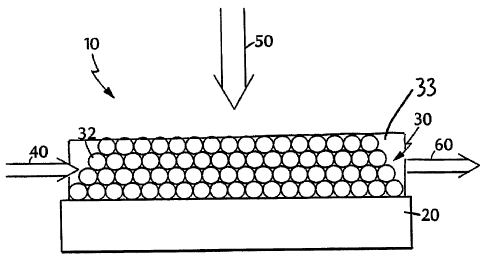
Referring to Figure 1, an amplifier 10 includes a substrate 20 and a gain
medium 30. Gain medium 30 includes a composite of nanocrystals 32 in a metal
oxide matrix 33. In operation, a user of amplifier 10 directs an input optical
radiation
beam 40 through gain medium 30 and provides an external optical radiation beam
50
to excite the gain medium to create a population inversion. Provided that the
energy
of input optical beam 40 overlaps the energies at which gain medium 30
facilitates
gain, amplifier 10 amplifies optical beam 40 to produce an amplified output
beam 60.
The general methodology for preparing nanocrystal-titanic composites is as
follows: The as-synthesized nanocrystals (see, C.B. Murray et al., J. ~9fner.
'hem.
Soc. 1993, I15, 8706, B.O. Dabbousi et al., J. Phys. Chem. B 1997,101, 9463)
are
stripped of their native TOPO cap by two or three precipitation/redispersion
cycles
from a butanol-hexane solution with methanol. The resulting powder is
evacuated
under vacuum and brought into a nitrogen-atmosphere glove box. The
nanocrystals
are then redispersed in a minimum volume of tetrahydrofuran and then mixed
with
ethanol and stoichiometric equivalents of tris-hydroxylpropylphosphine (tHPP)
and
titanium (IV) butoxide (TBOT). This solution was allowed to stir within the
glove
box at 60°C for at least 3-4 hours. A clear, fluorescent solution of
nanocrystal in a
titanic prepolymer results, which is then filtered and spin-coated onto a pre-
cleaned
glass microscope slide in a humidity controlled (~20 %) box. The resulting
film is
then transferred to a heating block at 200°C for 2 minutes. Finally,
the glass slide is
16
CA 02460796 2004-03-17
WO 03/025539 PCT/US02/29305
allowed to cool down rapidly to room temperature to yield a clear
nanocrystal/titania
composite film. The relative ratio of nanocrystals and tHPP/TBOT was
empirically
determined by the required refractive index of the composite film. The ratio
of
tHPP/TBOT and ethanol was determined by the desired film thickness. The film
thickness can also be controlled by the speed at which the films are spin
coated. More
complicated film geometries are synthesized by sequentially spin coating the
different
nanocrystal-titania prepolymer solutions and the buffer, neat titania layers
and
annealing the films between each successive spin-coating step.
The absorption and refractive index characteristics of the films were
characterized using a Cary spectrometer and a Gaetner ellipsometer,
respectively.
Interference fringes of the films, when coupled with film thickness, measured
independently using a profilometer, provide an estimate of the refractive
index of the
films. Volume fractions of nanocrystals within these composites were computed
from
absorption and profilometer measurements using previously calculated
absorption
cross-section values for the nanocrystals (see, L.A. Coldren, U.S. Pateht No.
4,896,35). The films were characterized using AFM for surface roughness and
distributions of surface cracks.
Optical investigations of the films were as follows: The films were studied
either directly in air, or mounted into a cryostat. The cryostat was then
either cooled
down to 80 K or kept at room temperature. The films were optically pumped
perpendicular to the wave-guiding direction using a 100 fs, regeneratively-
amplified
Ti-sapphire laser (400 nm), which is focused down into a stripe using a
cylindrical
lens. The wave-guided fluorescence is then collected using a fiber optic cable
normal
to the direction of excitation, dispersed in a spectrometer, and collected
using a liquid-
nitrogen cooled CCD camera.
Figure 2 shows an AFM scan of an optically clear nanocrystal-titania
composite after thermal annealing. The surface roughness (RMS) over a 13 ~,m x
13
~,m area is approximately 6 nm. Such roughness is on the order of the size of
the
nanocrystal stabilized (S nm diameter) within the composite. We do not see
macroscopic cracks or other defects over the scanned area, which would reduce
the
17
CA 02460796 2004-03-17
WO 03/025539 PCT/US02/29305
wave-guiding efficiency of the composite film and hinder the observation of
ASE.
Absorption spectra of composite films are combined with film thickness
measurements and absorption cross-sections for the nanocrystals (see, C.A.
Leatherdale, Ph.D. Dissertation, Massachusetts Institute of Technology,1999,
incorporated by reference in its entirety) to calculate the volume fraction of
nanocrystals in the films. Volume fractions of nanocrystals in these films can
be
tuned as high as 10-12%. Such volume fractions are higher than the
theoretically
required volume fractions (~1%) required for ASE as calculated by Klimov (see,
V.I.
Klimov et al., S'ciehce 2000, X90, 314, incorporated by reference in its
entirety), but
lower than the volume fractions achieved in close-packed nanocrystal films
(~20%).
We are able to reproducibly synthesize films over 1.5 cma substrates with a
thickness
that can be tuned from 0.2 to 0.7 ~,m. The variation in film thickness over
these
macroscopic distances is typically between 10-20 nm. Additionally, we are also
able
to tune the refractive index of nanocrystal-titania films from 1.65 to 1.82 by
tuning the
volume fraction of nanocrystals in the matrices.
Figure 3 demonstrates the appeal of using nanocrystals as the active gain
material by showing the wide spectral window within which the nanocrystal gain
profile can be tuned by using these nanocrystal-titania composites. Using the
same
stabilization chemistry, we exploit the size-dependent optical properties in
these
strongly quantum confined nanocrystals to synthesize nanocrystal-titania
composites
showing ASE from 560 nm to 650 nm. Figures 3A and 3B illustrate this
flexibility by
summarizing the optical response of a range of composite films at 80 I~ below
and
above the ASE threshold respectively. Figure 3A shows the normalized emission
spectra of different sized nanocrystals below the lasing threshold. The
linewidth of
the spontaneous emission peak in all these films is approximately 30 nm
(FWHM), a
linewidth that is indicative of the relatively narrow size-distribution of the
as-
synthesized nanocrystal. Absence of sub-bandgap, red trap luminescence also
indicates the retention of the optical properties of the constituent
nanocrystals
throughout the sol-gel processing. Labeled with arrows on the spontaneous
emission
spectra are the positions of the observed ASE peaks. Figure 3B shows the ASE
spectra from the same composite films above threshold. A dramatic reduction in
18
CA 02460796 2004-03-17
WO 03/025539 PCT/US02/29305
linewidths is quite apparent, as the FWHM of these ASE peaks is below 10 nm.
Also,
as is evident from Figures 3A and 3B, without exception the ASE peaks seen in
these
films are to the red edge of the spontaneous emission peak. Such behavior is
consistent with the expectation that the net gain should be highest only to
the red of
the fluorescence peak, where reabsorption losses are minimized. Such behavior
is
also consistent with experimental observations of gain from Klimov et al. on
close-
packed nanocrystal films (see, V.I. Klimov et al., Sciefzce 2000, 290, 314
incorporated
by reference in its entirety), but stands in contrast with observations from
others. See,
F. Gindele, Appl. Plays. Lett. 1997, 71, 2181, incorporated by reference in
its entirety.
The lack of a clear ASE signal (see, F. Gindele, Appl. Phys. Lett. 1997, 71,
2181,
incorporated by reference in its entirety), however, prevents reconciliation
of these
differing results.
The stability of nanocrystal-titanic wave-guides, as compared to self
assembled films, is next exploited to demonstrate ASE at room temperature
(RT).
While the presence of a temperature insensitive gain profile in such strongly
confined
nanocrystal has been theoretically predicted and observed, observation of RT
ASE has
been hindered by the instability of the close-packed films even at 80 K. In
the case of
nanocrystal-titanic films, however, rapid thermal annealing is expected to
reduce the
porosity by crosslinking and stabilizing the titanic matrix. See, L.A.
Coldren, U.S.
Patent No. 4, 896, 325, 1988, which is incorporated by reference in its
entirety. Such
stability is exploited to yield films showing ASE at room temperature in air.
Figure 4
shows the normalized emission spectra for the nanocrystal-titanic waveguides
above
and below threshold. A reduction in the emission linewidth is again evident
and the
ASE peak is located on the red-edge of the spontaneous emission peak. Such
observations portend well for the development of lasers assembled from
nanocrystal-
titania composites that, with suitable feedback mechanisms, will operate at
room
temperature.
Finally, the ease of preparing these films is exploited to produce more
complicated wave-guide structures, in which two different, high-refractive
index
nanocrystal-titanic layers are separated by a low-refractive index neat
titanic layer
19
CA 02460796 2004-03-17
WO 03/025539 PCT/US02/29305
(inset Figure 5). The presence of nanocrystals at such high volume fractions
increases
the refractive index of the neat titania film from ~1.6 to values as high as
1.8. Figure
4 reproduces the optical response at 80 K of one such composite film, where
one sees
a characteristic sharpening of the PL spectra at two spectrally distinct
regions (559 nm
and 624 nm), each corresponding to one of the nanocrystal-titania layers used
to build
up the heterostructure. The inset in Figure 5 shows the characteristic super-
linear
behavior at both ASE wavelengths as a function of the excitation intensity,
and the
ASE thresholds.are marked with arrows. It is important to note that such
simultaneous ASE behavior is not possible by simply mixing two different sized
nanocrystal within the same layer,for two reasons. First, mixing the different
sized
nanocrystal within the same layer reduces their individual volume fractions,
below
those necessary to observe ASE. Second, the nanocrystals have significant
absorption
cross-sections at energies higher than their band edge absorption state, a
feature that is
used to simultaneously pump these structures. Therefore, any gain presented by
the
smaller sized nanocrystal would be scavenged by absorption losses from the
larger
sized nanocrystal, resulting in ASE developing only at the longer wavelength.
Spatially separating the two nanocrystal-titania layers reduces these
absorption losses,
as the wave-guided light is confined to the individual layer itself. The
strength of the
chemical approach of this report is clearly summarized by the ease with which
these
layered composites are created. Such a structure represents a bottom up
approach to
rebuilding a broadband gain composite material using individual narrow gain
composites deposited sequentially in layers, but with the relative temperature
insensitivity of the observed gain.
~ther embodiments are within the scope of the following claims.