Note: Descriptions are shown in the official language in which they were submitted.
CA 02461037 2004-04-13
76224-22D
DIFFERENTIAL SIGNAL ELECTRICAL CONNECTORS
This is a divisional of copending Canadian Patent
Application Serial No. 2,392,322.
Background of the Invention
The invention relates to electrical connectors
and, more particularly, to modular electrical connectors
that provide signal paths for differential signals between
mother boards and daughter boards or other electrical
components.
Specialized electrical connectors may be used to
connect different components of an electrical system.
Typically, such an electrical connector connects a large
number of electrical signals between a series of daughter
boards to a mother board. The mother and daughter boards
are connected at right angles. The electrical connector is
typically modular. For example, a flat, planar metallic
lead frame contains several signal paths, each of which
bends about a right angle within the plane of the metallic
lead frame. The signal paths are assembled into an
insulated housing that also contains a planar ground plate
that provides a ground path and provides isolation between
signals. The module is further assembled with other similar
modules to form a connector capable of connecting a large
number of signals between components in an electrical
system.
Typically, the connectors attach to a printed
circuit board, e.g., a mother board, daughter board, or
back-plane. Conducting traces in the printed circuit board
connect to signal pins of the connectors so that signals may
be routed between the connectors and through
1
CA 02461037 2004-04-13
76224-22D
the electrical system. Connectors are also used in other
configurations, e.g., for interconnecting printed circuit
boards, and for connecting cables to printed circuit
boards.
Electronic systems generally have become more
functionally complex. By means of an increased number of
circuits, in the same space, which also operate at
increased frequencies. The systems handle more data and
require electrical connectors that ar electrically
capable of carrying these electrical signals. As signal
frecruencies increase there is a greater possibility of
electrical noise being generated by the connector in
forms such as reflections, cross-talk and electromagnetic
radiation. Therefore, the electrical connectors are
designed to control cross-talk between different signal
paths, and to control the characteristic impedance of
each signal path. In order to reduce signal reflections
in a typical module, the characteristic impedance of a
signal path is generally determined by the distance
between the signal conductor for this path and associated
ground conductors, as well as both the cross-sectional
dimensions of the signal conductor and the effective
dielectric constant of the insulating materials located
between these signal and ground conductors.
Cross-talk between distinct signal paths can be
controlled by arranging the various signal paths so that
they are spaced further from each other and nearer to a
shield plate, which is generally the ground plate. Thus,
the different signal paths tend to electromagnetically
couple more to the ground conductor path, and less with
each other. For a given level of cross-talk, the signal
paths can be placed clos.er together when sufficient
electromagnetic coupling to the ground conductors is
- 2 -
CA 02461037 2006-11-09
78496-5D
maintained.
An early use of shielding is shown in Japanese
patent disclosure 49-6543 by Fujitsu, Ltd. Dated
February 15, 1974. U.S. patents 4,632,476 and 4,806,107
(both assigned to AT&T Bell Laboratories) show connector
designs in which shields are used between columns of signal
contacts. These patents describe connectors in which the
shields run parallel to the signal contacts through both the
daughter board and the back-plane connectors. U.S. Patents
5,429,520, 5,429,521, 5,433,617, and 5,433,618 (all assigned
to Framatome Connectors International) show a similar
arrangement.
Another modular connector system is shown in US
Patents 5,066,236 and 5,496,183 (both assigned to AMP,Inc.),
which describe electrical modules having a single column of
signal contacts and signal paths arranged in a single plane
that parallels the ground plate. In contrast, U.S. Patent
5,795,191 describes an electrical module having electrical
signal paths arranged in two parallel planes that each
couple to a different ground plate.
It appears that the foregoing electrical
connectors are designed primarily with regard to single-
ended signals. A single-ended signal is carried on a single
signal-conducting path, with the voltage relative to a
common ground reference set of conductors being the signal.
For this reason, single-ended signal paths are very
sensitive to any common-mode noise present on the common
reference conductors. We have recognized that this presents
a significant limitation on single-ended signal use for
systems with growing numbers of higher frequency signal
paths.
Further, existing high frequency high density
3
CA 02461037 2004-04-13
76224-22D
connectors often require patterns and sizes of holes in
the attached printed wiring boards (PWB) that limit the
width and number of printed circuit signal traces that
may be routed through the connector footprint portion of
the PWB(s).
We have recognized that, predominantly in a
printed circuit backplane, it is highly desirable to have
the ability to route on each signal layer multiple traces
in various directions between particular patterns, rows,
or columns of holes in the connector footprint. We have
also recognized that in higher frequency backplane
applications, especially for long path lengths, the
ability to route wider traces can be used to reduce
conductor losses.
We have also recognized that better control of
cross-talk can be obtained by designing connectors for
differential signals. Differential signals are signals
represented by a pair of conducting paths, called a
"differential pair". The voltage difference between the
conductive paths represents the signal.
Differential pairs are known in such applications
as telephone wires and on some high speed printed circuit
boards. In general, the two conducting paths of a
differential pair are arranged to run near each other.
If any other source of electrical noise is
electromagnetically coupled to the differential pair, the
effect on each conducting path of the pair should be
similar. Because the signal on the differential pair is
treated as the difference between the voltages on the two
conducting paths, a common noise voltage that is coupled
to both conducting paths in the differential pair does
not affect the signal. This renders a differential pair
less sensitive to cross-talk noise, as compared with a
- 4 -
CA 02461037 2004-04-13
76224-22D
single-ended signal path. We have invented an electrical
connector well suited for carrying differential pairs.
In addition, it is advantageous to have
symmetrical, balanced electrical characteristics for the
two conductive paths of a differential pair. Because
current connectors have signal paths of different lengths
(as shown in FIGS. 2 and 3), the electrical delay of each
path is not equal, which can degrade the differential
signal quality by inducing skew. it would be highly
desirable to have a differential connector that has
balanced paths.
Further, it would be desirable to have a
differential connector module that is compatible with
existing modular connector components. It would also be
desirable to have a connector with a circuit board hole
pattern that supports multiple wide signal traces and
improved routability.
Summary of the Invention
One aspect of the invention is an electrical
connector module for transferring a plurality of
differential signals between electrical components. The
module has a plurality of pairs of signal conductors with
a first signal path and a second signal path. Each
signal path has a contact portion at each end of the
signal path, and an interim section extending between the
contact portions. For each pair of signal conductors, a
first distance between the interim sections is less than
a second distance between the pair of signal conductors
and any other pair of signal conductors of the plurality.
Another aspect of the invention is an electrical
connector module for conducting differential signals
between electrical components, the connector module
having opposing sides terminating along an edge. The
- 5 -
CA 02461037 2004-04-13
76224-22D
module contains a pair of signal conductors optimized for
coupling to the differential signal. The conductors are
disposed in the module. Each one of the conductors has a
contact portion that is laterally spaced along the edge of
the module. Surface portions of the pair of conductors pass
from the contact portions through the module in a
substantially overlaying relationship along a direction
extending through the sides of the module.
Each embodiment of the invention may contain one
or more of the following advantages. The impedance of each
differential signal path is matched. Each signal path of
the pair of differential signal conductors is of equal
electrical length. The pairs of differential signal paths
can be spaced closer together. The spacing of each pair of
differential signal conductors from other pairs reduces
cross-talk within the connector. The pair of differential
signal conductors can couple to the ground plate to allow
other pairs of differential signal conductors to be placed
closer to the signal paths without inducing cross-talk. A
portion of the shield plate can extend between each of the
pairs of differential signal conductors. Noise within each
pair of differential signal conductors is reduced. The
routing of signal traces is efficient. The grounding
contact portions can extend between the contact portions of
the signal conductors and allow the signal traces to extend
in a direct path through a routing channel. The routing
channel can be wide and straight.
According to another aspect the invention provides
a printed circuit board for receiving differential pair
contact tail portions of a connector, the printed circuit
6
CA 02461037 2004-04-13
76224-22D
board comprising: at least one ground plane layer having
pairs of apertures configured to receive the differential
pair contact tail portions of the connector; and for each
pair of apertures corresponding to a differential pair, an
area surrounding the pair of apertures is free of the ground
plane layer and each aperture of the pair is electrically
isolated from the other.
According to yet another aspect the invention
provides a printed circuit board for receiving differential
pair contact tail portions of a connector, the printed
circuit board comprising: a surface exposing pairs of
apertures configured to receive the differential pair
contact tail portions of the connector; ground plane layers;
for each pair of apertures corresponding to a differential
pair, an area surrounding the pair of apertures is free of
the ground plane layers and each aperture of the pair is
electrically isolated from the other; and for the pairs of
apertures, an area between adjacent pairs of apertures
includes the ground plane layers.
Brief Description of the Drawings
FIG. 1 is a perspective view of a system according
to the invention wherein a set of modular connectors are
assembled between a mother board and a daughter board;
6a
CA 02461037 2004-04-13
76224-22D
FIG. 2 is a schematic view of a prior art signal
path metal lead frame that can be used in the assembly of
a modular electrical connector wherein the signal paths
are equally spaced and are not arranged in differential
pairs;
FIG. 3 is a schematic view of a signal path metal
lead frame that is used in the construction of a modular
connector wherein the signal paths are arranged in pairs
of differential signal conductors in a single plane;
FIG. 4 is a schematic view of still another
embodiment of a signal path metal lead frame that is used
in the construction of a modular connector wherein the
signal paths are arranged in pairs of differential signal
conductors in a single plane;
FIG. 5 is a perspective view of a ground plate
compatible for use with the signal path metal lead frame
of FIG. 4, wherein contact portions of the ground plate
are extendable between contact portions of the signal
path metal lead frame;
FIG. 5A is a perspective view of a pin header
incorporating the ground plate of FIG. 5;
FIG. 6 is a perspective view of an arrangement of
signal paths according to the prior art wherein the
signal paths are arranged in two parallel planes, each
signal path in one plane inductively coupling with a
first ground plate (not shown) and each signal path in
the other plane coupling with a second ground plate (not
shown);
FIG. 7 is a perspective view of another embodiment
of signal paths arranged in pair of differential signal
conductors, wherein the signal paths are arranged in two
parallel planes; -
FIG. 8 is a front view of yet another embodiment
- 7 -
CA 02461037 2004-04-13
76224-22D
of signal paths arranged as a pair of differential signal
conductors, wherein the signal paths are arranged in two
parallel planes;
FIG. 9 is a side view of the signal paths of FIG.
8; FIG. 10 is a schematic view of connector module
with balanced electrical properties;
FIG. 11A is a sketch illustrating a prior art
circuit board signal launch; and
FIG. 11B is a sketch illustrating an improved
circuit board signal launch.
Description of the Preferred Embodiments
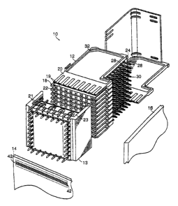
Referring to FIG. 1, an electrical system 10
includes a modular connector 12 that connects a backpi-ane
14 to a daughter board 16. The connector 12 includes a
plurality of connector modules 18 capable of connecting a
set of electrical signals, either differential signals,
non-differential signals, or both types of signals.
For example, if assembled as described below, the
electrical connector module 18 can conduct a pair of
differential electrical signals between electrical
components of the system 10 such as the mother board 14
and the daughter board 16. Each connector module 18 has
opposing sides 20, 22 that are aligned in parallel. The
sides 20, 22 each terminate along an edge 24 of the
connector module 18. (As shown, edge 24 is a planar
surface section 28. However, other configurations are
possible.) A set of connecting pins 28 extend from the
edge 24. Shields (not shown) may be placed between
modules 18.
It should be noted that in a preferred embodiment,
the openings 19 in each module 18 are evenly spaced.
Likewise, the contact tails 28 are evenly spaced.
- 8 -
CA 02461037 2006-11-09
78496-5D
Referring to FIG. 2, a metal lead frame 50 defines
eight non-differential signal paths 52a-52h for use in
connector module 18. The metal lead frame 50 is stamped
from a thin, metallic, planar member to include carrier
strips 56 that support the signal paths 52a-52h prior to and
during assembly of the electrical connector module 18. When
the signal paths 52a-52h are fully integrated into the
electrical connector module 18, support sections 56 are
disconnected from the signal paths 52a-52h, and each signal
path 52a-52h is disconnected from the other paths 52a-52h.
U.S. Patent No. 5,980,321, High Speed, High Density
Electrical Connector, filed February 7, 1997, discloses an
electrical connector that incorporates the metal lead frame
50.
Referring to FIG. 3, a similar metal lead frame
100, for use in module 18, defines eight signal paths 102a-
102h. However, the paths 102a-102h are grouped into four
pairs of differential signal conductors 104a-104d. The
metal lead frame 100 is stamped with a thin, metallic,
planar member that supports the signal paths 102a-102h prior
to and during assembly of the electrical connector module
18. When the signal paths 102a-102h are fully integrated
into the electrical connector module 18, support sections
106 are disconnected from the signal paths 102a-102h, and
each signal path 102a-102h is disconnected from the other
signal paths 102a-102h inside the electrical connector
module 18.
Each one of the signal paths 102a-102h includes a
pair of contact portions 112, 114, and an interim section
116 between the contact portions. The contact portions 112,
114 are connecting pins that connect the module 18
9
CA 02461037 2004-04-13
76224-22D
to the electrical components of the system 10. Contact
portions 112 are shown as two parallel members. These
members can be folded to form a box contact as in the
prior art. The box contact acts as a receptacle for a
pin 21 from the backplane. However, separable contact
regions of many shapes are known and are not crucial to
the invention.
In the present embodiment, the contact portions
112 of the signal 'paths .102a-102h are laterally and
equidistantly spaced along the edge 118 of the metal lead
frame 100. In a preferred embodiment, the spacing is
.030". Typically, when attached as part of the system 10,
the lateral spacing is in a vertical direction. Both the
contact portions 112, 114 extend from the housing 32 of
the module 18. The external structure of module 18 is
identical to other modules which are not specifically
designed to conduct differential signals. Therefore, the
modules 18 are interchangeable with other modu'Les, and
the connector 12 can be configured with different types
of modules which allow the connector 18 to conduct both
differential and non-differential signals.
The interim sections 116 of each signal path 102a-
102h are aligned in a single plane 120, typically a
vertical plane. Therefore, surface portions 118 of each
interim section 116 in the pair of conductors 104a-104d
are substantially overlaid in the vertical plane.
The each signal path 102a-102h is coupled with a
second signal path 102a-102h in pairs of differential
signal conductors 104a-104d. For example, signal paths
102a, 102b form the pair of differential signal
conductors 104a; the signal paths 102c, 102d form the
pair of differenti=al signal conductors 104b; the signal
paths 102e, 102f form the pair of differential signal
- 10 -
CA 02461037 2004-04-13
76224-22D
conductors 104c; the signal paths 102a, 102h form the
pair of differential signal conductors 104d. Each
signal path 102a-102h of each pair of differential signal
conductors 104a-104d is coupled to the corresponding
signal path 102a-102h of the pair 104a-104d. The
coupling results because the distance 108 between the
pairs of differential signal conductors 104a-104d is
small relative to the distance 110 between adjacent pairs
of differential signal conductors 104a-104d. The interim
sections 116 of the pairs of sianal conductors 104a-104d
are arranged as close.together as possible while
maintaining differential impedance. One of the interim
sections 116 of each pair 104a-104d has curved sections
122, 124 that curves toward the other interim section 116
of the pair 104a-104d. Between the curved sections 122,
124, the pair of conductors 104a-104d tracks together
along most of the interim sections 116.
The curved sections 122, 124 decrease the distance
108 between interim sections 116 of each pair 104a-104d,
increase the distance 110 between adjacent pairs 104a-
104d, and tend to equalize the length of each interim
section 116 of the pair 104a-104d. This configuration
improves the signal integrity for differential signals
and decreases cross-talk between differential pairs 104a-
104d and reduces signal skew.
Other embodiments are within the scope of the
invention.
For example, referring to FIG. 4, a metal lead
frame 100 includes six rather than eight signal paths
202a-202f. The signal paths are arranged in three pairs
204a-204c. In essence, metal lead frame 200 is identical
to metal lead frame 100 except that the equivalent of two
signal paths 102c, 102f have been removed. The remaining
- 11 -
CA 02461037 2004-04-13
76224-22D
traces have to be aligned in pairs as before, with the
spacing between the interim sections of the signal paths
in a pair less than the spacing between the contact
portions. Two spaces 208, 210, which are vacated by the
signal paths 102c, 102f, lie between contact portions
214.
Referring also to FIG. 5, a ground plate 220
contains a main body 230, resilient connecting tabs 224,
and contact portions 226, 228. Ground plate 220 is
intended to be used in place of ground plate 23 (FIG.1),
particularly in conjunction with the embodiment of FIG.
4.
When a connector 12 is fully assembled and mated
with connector 13, the ground plate 222 is parallel to
the signal paths 202a-202f. The contact portions 226,
288 are aligned with the contact portions 212 of the
signal paths 202a-202f. The contact portions 226, 228
are each at corresponding right angles to the main body
230 and extend between the contact portions 212 within
corresponding spaces 208, 210.
FIG. 5A shows the backplane module 13' including
the shield member 220. There are columns of signal pins
521. Each column contains six signal pins 521, to
correspond to the six mating contacts 212. There is no
signal pin in backplane connector 13' corresponding to
spaces 208 and 210 (FIG. 4). Rather, contact portions
226 and 228 are inserted into the spaces that correspond
to- spaces 208 and 210. As a result, there are eight
contact tails in each column - six corresponding to
signal pins 521 and two being appending contact tails 226
and 228. The spacing between the contact tails is
uniform, illustrated as dimension P in FIG. 5A.
This arrangement of contact tails means that the
- 12 -
CA 02461037 2004-04-13
76224-22D
spacing between adjacent columns is a dimension D. The
spacing D is dictated by the spacing between signal pairs
521 in adjacent columns.
By contrast, in backplane connector 13 (FIG. 1),
the space between columns of contact tails for signal
pins is occupied by contact tails for a shield plate.
When a backplane connector is attached to
backplane, a hole must be made for each contact tail. No
signal traces can be routed in the backplane near holes.
Thus, to space signal traces across a backplane, the
traces generally run in the spaces between columns of
contact tails. In the embodiment of FIG. 5A, the spacing
D represents a wide routing channel for signal traces.
Thus, the signal traces can be made wider and therefore
have lower loss. The traces can also be made straighter
because they do not have to jog around ground holes in
the channels between signal contact tails. Straighter
traces result in fewer impedance discontinuities, which
are undesirable because they create reflections. This
feature is particularly beneficial in a system carrying
high frequency signals. Alternatively more traces could
be routed in each layer, thereby reducing the number of
layers and saving cost.
Referring to FIG. 6, a set of prior art signal
paths 300a-300h for use in a modular electrical connector
have interim sections 302 that are aligned along two
different parallel planes 320, 322. Half of the interim
sections are aligned along each corresponding plane.
Contact portions 314 are aligned in a third central
plane. Contact portions 312 lie in separate planes and
are aligned with the third central plane. Thus, when
fully assembled, each interim section 302 lies closer to
a ground plate than to another of signal paths 300a-300h.
- 13 -
CA 02461037 2004-04-13
76224-22D
Referring also to FIG. 7, the signal paths of FIG.
6 are adapted to provide a set of differential signal
conductors 304a-304d. Each conductor of the pairs 304a-
304d includes a pair of contact portions 332, 334 and
interim sections 336, 337 extending between contact
portions 332, 334. Each pair of interim sections 336,
337 has a corresponding surface 338, 339 that overlays
the other corresponding surface 338, 339. The surfaces
338, 339 overlay each other in a direction that extends
through the sides 326, 328 of an electrical connection
module 303, shown in FIG. 6. Thus, relative to the pairs
104a-104d of FIG. 3 which typically have overlying
surfaces 118 in the vertical direction, the pairs 304a-
304d typically have overlying surfaces 338, 339 in the
horizontal direction. (The comparison between the pairs
104a-104d and the pairs 304a-304d is relative, and the
surfaces 338 may overly in directions other than
horizontal.)
However, unlike the paths 300a-300h depicted in
FIG. 6, interim section 336 of each pair 304a-304d lies
closer to corresponding interim section 337 of each pair
304a-304d than to a ground plate or another pair of
signal conductors 304a-304d. Therefore, each pair of
conductors 304a-304d couples to the corresponding
conductor of the pair 304a-304d to reduce noise.
The differential pairs of signal contacts will,
preferably be held in an insulative housing, which is not
shown. The contacts might be positioned as shown in FIG.
7 and then insulative material could be molded around the
interim sections of the contacts. To achieve appropriate
positioning of the contact members, a plastic carrier
strip might be molded around the contact members in one
plane. Then, the contact members in the other plane
- 14 -
CA 02461037 2006-11-09
78496-5D
might be overlaid on the carrier strip. Then, additional
insulative material could be molded over the entire
subassembly.
An alternative way to form an insulative housing
around the contact members in the configuration shown in
FIG. 7 would be to mold the housing in two interlocking
pieces. One piece would contain the signal contacts in one
plane. The other piece would contain the signal contacts in
the other plane. The two pieces would then be snapped
together to form a module with the signal contacts
positioned as in FIG. 7. This manufacturing technique is
illustrated in US patent 5,795,191. However, that patent
does not recognize the desirability of positioning the
interim sections of the signal contacts in the two pieces of
the subassembly so that, when the two pieces are assembled,
the signal contacts will overlay to create differential
pairs.
Referring also to FIGS. 8-9, an alternate
arrangement of signal paths includes pairs of signal
conductors 304' (here one pair being shown). Like the
signal paths 300a-300h of FIG. 6, each conductor 304' of the
pair extends toward the corresponding side 326, 328 of a
module 303'. However, unlike the signal paths 300a-300h,
surfaces 318' of the pair of signal conductors 304' are
respectively jogged to have overlaying surfaces 338', 339'
in a direction that is perpendicular to the sides 326, 328
of the module 303'. Thus, like the pairs of conductors of
FIGS. 3, 4 and 7, the distance between conductors 304' is
smaller than the distance from the pair of conductors 304'
to other similar pairs of conductors. Also, like the
contact portions 312 of FIG. 6, the contact portions 312',
314' all lie in a third
CA 02461037 2004-04-13
76224-22D
central plane. In comparison, the contact portions 332
shown in FIG. 7 and contact portions 314 shown in FIG. 6
lie in two distinct planes.
As another alternative, it is not necessary that
shield plates be used with the differential connector
modules as described above.
FIG. 10 shows an alternative embodiment for a
differential connector module 510. As described above, a
lead frame containing signal contacts is formed into a
module by molding plastic 511 around the interim portions
of the lead frame. In the module of FIG. 10, windows
512A, 512B and 512C are left in the plastic above the
long lead in each pair. These windows serve to equalize
the delay for signals traveling in the leads of each
pair. As is known, the speed at which a signal
propagates in a conductor is proportional to the
dielectric constant of the material surrounding the
conductor. Because air has a different dielectric
constant that plastic, leaving the windows above the long
leads, makes the signals in those leads move faster. As
a result, the time for a signal to pass through the long
lead and the short lead of the pair can be equalized.
The length of each window 512A...512C depends on
the differential length between the long leg and the
short leg of the pair. Thus, the size of the window
could be different for each pair. Also, it is possible
that multiple windows might be included for a pair.
Further, it is not necessary that the window be filled
with air. The window could be formed with a material
having a different dielectric constant than the rest of
plastic 511. For example, a plastic with a low
dielectric constant could be molded over portions of the
long contacts in each pair in the window regions. Then,
- 16 -
CA 02461037 2004-04-13
76224-22D
a plastic with a higher dielectric constant could be over
molded to form the plastic housing 511. Also, it is not
necessary that the "window" extend all the way to the
surface of the conducting signal contact. The "window"
could be partially filled with plastic and partially
filled with air, which would still have the effect of
lowering the effective dielectric constant of the
~material above the long leg.
One drawback of placing a window in the dielectric
material is that it also changes the impedance of the
signal contact in the region below the window. Changes
in impedance along a signal conductor are often
undesirable because signal reflections occur at the
discontinuities. To counter this problem, other
adjustments can be made to keep the impedance constant
along the length of the signal conductors. One way that
the impedance can be kept constant is by changing the
width of the signal conductors. In FIG. 10, the signal
conductors are shown with a width of T1 in one region and
a broader width T, in the region of the windows. The
exact dimensions are chosen to match the impedance based
on the relative dielectric constant between the two
regions. The technique of altering the width of the
signal contacts in window regions is useful regardless of
why the window is formed in the connector and is not
limited to windows formed to equalize delay. For
example, some prior art connectors use windows over
substantial portions of all the signal contacts to
increase impedance of all the signal contacts.
FIG. 11A and 11B show an alternative embodiment
that can be used to increase the effectiveness of a
differential connector. FIG. 11A illustrates a portion
of a backplane 600 to which a connector might be
- 17 -
CA 02461037 2004-04-13
76224-22D
attached. There are columns of holes 602 in backplane
600. The contact tails of the connector would be
inserted into these holes to affix the connector to the
backplane. One or more ground plane layers 604 are
included within backplane 600. The ground plane layers
are not deposited around the holes to avoid shorting out
the connections made in the hole to leave exposed areas
606. However, in the prior art configuration shown in
FIG. 11A, there is ground plane material deposited
between the holes 602. FIG. 11B shows a backplane
printed circuit board adapted for use with a differential
connector. Ground plane layer 604 is deposited to leave
an exposed area around the holes 602 that form a
differential pair. In this way, there is no ground plane
layer between the two holes of a differential pair.
Consequently, the common mode coupling between the two
conducting elements of the differential pair is improved.
Also, it should be appreciated that numbers and
dimensions are given herein. Those numbers are for
illustration only and are not to be construed as
limitations on the invention. For example, connectors
with 6 and 8 rows are illustrated. However, any number
of rows could be conveniently made.
Also, it was described that shield plates could be
used. Grounding members that are not plate shaped could
also be used. The grounding members could be p?aced
between pairs of conducting elements. In addition, the
shields do not need to be planar. In particular, FIG. 3
and FIG. 4 illustrate a connector configuration in which
there are spaces between differential pair. To increase
the isolation between the differential pairs, tabs could
be cut out of the shield plates and bent out of the plane
of the plate to provide greater isolation between pairs.
- 18 -
CA 02461037 2004-04-13
76224-22D
It should also be recognized that the invention is
illustrated by a right angle, press-fit, pin and socket
connector. The invention is not useful simply in right
angle applications. it could be used in stacking or
mezzanine connectors. Nor is the invention limited to
press-fit connectors. It could be used with surface
mount or pressure mount connectors. Moreover, the
invention is not limited to just pin and socket style
connectors. Various contact configurations are known and
the invention could be employed with other contact
configurations.
- 19 -