Note: Descriptions are shown in the official language in which they were submitted.
CA 02461097 2004-03-22
Od- 3-17118:16 ;HOSODA&Partners Cowlings , ~ 5
FNGK0219PCT-CA
SPECIFICATION
CERAMIC LAMINATED SINTERED BODIES, A METHOD OF
PRODUCING THE SAME, ELECTROCHEMICAL CELLS, CONDUCTIVE
INTERCONNECTORS FOR THE SAME AND ELECTROCHEMICAL
DEVICES
BACKGROUND OF THE INVENTION
1. Field of the Invention
The present invention relates to a ceramic laminated sintered body, a
method of producing the same, an electrochemical cell, a conductive
interconnector for electrochemical cell and an electrochemical device.
2. Related Art Statement
Solid oxide fuel cells are generally divided into two categoxiesi planar
and tubular types. In planar type solid oxide fuel cells, a power generating
stack is formed by alternately laying so-called separators and power
generating
layers. In Japanese patent publication No. 5-54897A, an anode and a cathode
are respectively formed on the sides of solid electrolyte film to prepaxe a
power
generation layer. Then a thin film containing ceramic powder and an organic
binder is sandwiched between this power generation layer and an
interconnector to obtain an assembly, which is then heat treated so that the
power generation layer and the interconnector are joined with each other.
The inventors have studied to produce an SOFC operating at a
relatively low temperature, for example, at about 800 °C. In such kind
of
SOFC has, for example, thick fuel and air electrodes are provided on both
surfaces of a thin film of 3 mole percent yttria stabilized zirconia,
respectively.
The thin film of zirconia has an extremely small thickness of, for example,
about
1
CA 02461097 2004-03-22
04- 3-17:18:16 ;HOSODA&Partners Gowlm g5 , p 6
FNGK0219PCT-CA
,um. It is thus required that the solid electrolyte film has excellent air-
tightness. In prior arts, however, it has not been sufficiently studied a
technique for laminating and then co-sintering the thin solid electrolyte film
having high air-tightness with the ceramic electrode having a large thickness
and high porosity.
So called absorption dipping method is known as the technique.
According to the method, slurry for zirconia is absorbed and adhered onto the
surface of an air electrode and subjected to co-sintering.
It is further known to sinter a green sheet of a solid electrolyte to
produce a dense film of the solid electrolyte (Japanese patent No. 318390&).
It
is described that the film has a thickness of 100 ,u m to lmm and a
transmittance of nitrogen gas of zero.
It is further known to form an yttria stabilized zirconia film (solid
electrolyte hlm) by ion plating on an air electrode made of a porous sintered
body (Japanese patent publication 2000- 62077A). It is described that the film
has a leakage rate of helium gas of 1 x 10~ 7 to 1 x 10~ g atm ~ cc/s.
It is also known a method of forming an yttria stabilized zirconia film
on a polymer sheet, laminating the polymer sheet on a green sheet of an
electrode, and sintering the green sheet (Japanese patent No. 3220314). The
polymer sheet is disappeared during the sintering step.
SUMMARY OF THE INVENTION
It is, however, found that the zirconia film obtained by absorption
dipping method has many pores and defects therein when observed
microscopically. It is required to reduce the thickness of the solid
electrolyte
film and to maintain the air tightness of the solid electrolyte at the same
time,
for improving the generation efficiency of the SOFC. A manufacturing
2
CA 02461097 2004-03-22
04- 3-17;18:16 ;HOSODA&Parlners Cowlings , # 7
FNGK0219PCT-CA
technique satisfying the above requirements has been demanded. According to
absorption dipping method, it is difficult to control the thickness of the
zirconia
film at a uniform value to result in local deviation of the thickness. The
deviation of thickness of the zirconia film results in local deviation in the
performance of generation of the SOFC so that the overall generation
efficiency
is lowered.
The sheet sintering method described in Japanese patent No.
3183906 may provide a dense solid electrolyte film having a thickness as small
as about 100 ,u m. The cell having a solid electrolyte film having a thickness
of 100 ,u m to 1 mm exhibits, however, a limit in improving the efficiency of
the
cell. It is difficult to produce a solid electrolyte film having a thickness
of, for
example, about 25 ,u m.
Although the he above method of forming a solid electrolyte film by
ion plating is applicable for forming a film with a small axes, it is
difficult and
impractical to form a film with an area sufficiently large for practical
applications on the viewpoint of an actual manufacturing pxocess.
Further in a process for forming a solid electrolyte film by printing on
a substrate, the resulting film has many defects, for example, due to the
effects
of irregularity on the surface of the substrate. It is thus difficult to
obtain a
dense film having a large area.
According to the method described in Japanese patent No. 3220319:,
the polymer sheet is disappeared at a temperature lower than the starting
temperature of the sintering of the green sheet. The green sheet does not have
a sufficiently high strength so that defects may be easily induced in the
film.
As described above, it is desired a dense solid electrolyte film having a
large area and a thickness as small as possible for improving the e~ciency of
an
electrochemical cell. It is, however, difficult to reduce the thickness and
3
CA 02461097 2004-03-22
OG- 3-17:18:16 ;HOSODA&Pa « ners Cowlings , p 8
FNGK0219PCT-CA
porosity of a solid electrolyte film on the viewpoint of an actual
manufacturing
process as described above. It has thus not been studied how the efficiency of
an electrochemical cell is actually improved by reducing the thickness of the
solid electrolyte film.
The inventors have successfully produced a relatively dense solid
electrolyte film having a Iarge area and an electrochemical cell, such as a
solid
oxide fuel cell using the film. They have further performed a test of power
generation for the cell as described later. It is thus found that the effect
of the
air tightness of the solid electrolyte film on the generation efficiency is
relatively small so that a high degree of air tightness may not be necessary
for
further improving the efficiency. Based on the findings, it should have been
relatively easy to increase the area and reduce the thickness of the solid
electrolyte film at the same time.
The inventors have further studied the technique and found the
followings. That is, the air tightness of the solid electrolyte film having a
large
area and small thickness is reduced to a value lower than a specific value, it
is
proved that the cell is deteriorated to result in a considerable reduction of
generation efficiency after repeating activation and termination of the
operation
of the cell.
An object of a first aspect of the present invention is to apply a
laminated sintered body of ceramic porous and dense bodies on an
electrochemical cell, and to improve the operational e~ciency of the cell and
to
prevent the deterioration of the cell after the activation and termination of
operation is repeated so as to prevent the reduction of the operational
efficiency
of the cell.
An object of a second aspect of the present invention is to produce a
laminated sintered body of ceramic porous and dense bodies on an
4
CA 02461097 2004-03-22
04- 3-17:18:16 :HOSODA&Partners Cowlings . # 9
FNGN0219PCT-CA
electrochemical cell, and to reduce defects and pores in the dense body and to
produce the dense body having a constant thickness.
When a plurality of unit cells and separators are laminated in turns
to produce a stack (stacked cells), a material for the separator is exposed to
fuel
and oxidizing gases. The material for the separator should be resistive
against
the gases at an operational temperature of the cell of, for example, 800 to
1000 °C, and should have a specific volume resistivity as low as
possible at the
operational temperature of the cell. Materials satisfying the above
requirements are relatively rare and lanthanum chxomite is frequently used
until now.
When many planar unit cells and separators are laminated to
produce a stacked cell, it is required that each of the unit cell and
separator is a
self-standing structural body without the need of providing another structural
body for supporting. It is considered that the separator is made of a metal
for
making a self standing separator. It is found that an appropriate metal is
xare
which is not oxidized ovex a long time under aix at a high temperature of, for
example, 1000 °C. When a separator made of nickel or a nickel based
alloy
resistive against a fuel gas is used, nickel or nickel based alloy is
gradually
oxidized over a long time period so as to reduce the conductivity of the
separator
and generation efficiency.
On the other hand, when a separator is made of lanthanum chromite
having resistance against fuel and oxidizing gases at a temperature of 800 to
1000 °C, it is necessary to increase the thickness of the separator for
providing a
self standing separator. Lanthanum chromite, however, has a relatively large
electrical resistance, so that a loss of voltage is increased due to an
internal
resistance in the separator to lower the generation output. Particularly when
any separators and unit cells are laminated, the effects of the voltage loss
is
CA 02461097 2004-03-22
04- 3-17;18:16 :HOSODA&Partners Cowlings . # 10
FNGK0219PCT-CA
considerable.
An object of a third aspect of the present invention is, in an
electrochemical device produced by laminating electrochemical cells and
conductive interconnectors for connecting the cells in turns, to provide a
self
standing interconnector, to prevent reduction of operational efficiency due to
oxidation and corrosion of the interconnector and to reduce an internal
resistance in the interconnector to reduce the voltage loss.
The first aspect of the present invention provides a laminated
sintered body having a ceramic porous body having a thickness of 300 ,u m or
larger and a ceramic dense body having a thickness of 25 ,u m or smaller. The
laminated sintered body has a helium leakage rate of 10 6 Pa ~ m3/s or lower.
The inventors have produced a thin and dense film, such as a solid
electrolyte film, having a thickness of 25 ,u m or smaller and a large surface
area on a ceramic porous body and measured the operational efficiency of a
cell,
such as the generation output of an SOFC, as described later. When the
thickness of the solid electrolyte film is lowered and the surface area is
increased, the air-tightness of the film inevitably tends to be reduced and
the
helium leakage rate elevated. It is very difficult to prevent the tendency due
to
the limit of actual manufacturing processes, as described above.
The inventors thus have variously changed the helium leakage rate
and studied the relationship between the rate and generation output. Such
test of the relationship has not been clearly studied yet. This is because it
has
been difficult to reduce or control the helium leakage rate of a solid
electrolyte
film having a large surface area and a thickness of 25 ,u m or smaller at the
same time due to the limit of production. The inventors have enabled such
study of the relationship by utilizing the production method according to the
second aspect of the present invention described later. It is finally found
that
6
CA 02461097 2004-03-22
04- 3-17;18:16 :HOSODA&Partners Cowlings , ~ 11
FNGK0219PCT-CA
the influence of an increase of the helium leakage rate of a solid electrolyte
film
on the generation output is not considerable.
That is, although the helium leakage rate is elevated as the solid
electrolyte film is thinner and the surface area is larger, a reduction in the
generation output proved to be not considerable considering the increase of
the
helium leakage rate. The generation output can be thus improved by lowering
the thickness and increasing the surface area of the solid electrolyte film.
It is
thus considered that the reduction of generation output due to an increase of
the helium leakage rate can be easily compensated.
The inventors have further investigated, and found the followings.
That is, when the helium leakage rate of the solid electrolyte film exceeds a
specific value, the operational efficiency of the cell may be reduced after
the
initiation and termination of the operation of the cell is repeated. Far
example,
the generation output of an SOFC may be considerably lowered compared with
an initial output. Since the initial output is not so lowered in this case,
the
reduction of the output is not correlated with the increase of gas leak during
the
generation process.
The inventors have further investigated and found the followings.
For example, when the operation of an SOFC is terminated, the supply of a fuel
gas is terminated, and an inert gas such as nitrogen and argon, or an inert
gas
containing a small amount of a fuel for imparting weak reductive property is
supplied instead of the terminated fuel gas. If a trace amount of an oxidizing
gas is leaked to the side of a fuel electrode, a partial pressure of oxygen in
the
side of the fuel electrode is elevated to result in the deterioration of the
fuel
electrode. For example, nickel component in the fuel electrode may be
oxidized.
A high concentration of fuel gas is supplied to the fuel electrode
7
CA 02461097 2004-03-22
04- 3-17:18:16 ;HOSODA&Parcners Cowlings , p 12
FNGK0219PCT-CA
during the subsequent operation, the once oxidized fuel electrode, for example
nickel oxide component contained therein, should have been reduced again. It
has been considered that the fuel electrode can be fully recovered. It is
found
that, in actual operation, the microscopic state of the fuel electrode is
changed
after the oxidation and reduction processes of the fuel electrode are
repeated, so
that desirable microstructure as the fuel electrode is gradually lost.
The inventors have studied the helium leakage rate of a dense thin
film of a laminated sintered body constituting a cell, based on the above
discovery, for preventing the deterioration of the microstructure of the cell
after
the initiation and termination cycles of the cell are repeated. It is finally
found that the deterioration of the cell after the initiation and termination
cycles are repeated can be prevented, by lowering the helium leakage rate to a
value of 10 s Pa ~ m3/s or lower.
The helium leakage rate of the laminated sintered body may
preferably be 10Y7 Pa ~ m3/s or lower on the viewpoint.
Further, the area of the laminated sintered body may preferably be
60 cm2 or larger for improving the operational efficiency of the cell.
The laminated sintered body of the first aspect of the present
invention may be applied to a solid electrolyte film and electrodes
constituting a
cell. Alternatively, the laminated sintered body may be applied as an
interconnector for connecting cells, The embodiments will be described later.
A second aspect of the present invention provides a method of
producing a laminated sintered body having a ceramic porous body having a
thickness, of 300 ,u m or larger and a ceramic dense body having a thickness
of
25 ,u m or smaller. According to the method, a green body for the porous body
and a green body for the dense body are laminated, and subjected to pressure
molding by cold isostatic pressing to obtain a pressure molded body, which is
8
CA 02461097 2004-03-22
04- 3-17;18:16 ;HOSODA&Par2ners Cowlings , p
FNOK0219PCT-CA
then sintered to obtain the laminated sintered body.
For producing a laminated body having a ceramic porous body having
a larger thickness and a thin ceramic dense body, the green bodies for the
dense
and porous bodies are laminated and subjected to pressure molding by cold
isostatic pressing, as described above. It is thus possible to reduce the
thickness of the dense body and to prevent defects and pores in the dense body
after the sintering process. Further, the thickness of the dense body can be
made uniform as a whole according to the following mechanism.
According to the second aspect of the present invention, in producing
the laminated sintered body having ceramic porous and dense bodies, it is
possible to reduce defects and pores in the dense body and to make the
thickness of the dense body constant.
Further, according to the above method, it becomes possible to
produce the laminated sintered body, according to the first aspect of the
present
invention, having a large area, a small thickness and low helium leakage rate.
A third aspect of the present invention provides a conductive
interconnector for connecting a plurality of electrochemical cells. The cell
has
a first electrode contacting a first gas, a second electrode contacting a
second
gas, and a solid electrolyte film provided between the first and second
electrodes.
The conductive interconnector has a ceramic substrate made of a material
having resistance against the first gas at an operational temperature of the
electrochemical cell, and a ceramic film formed on the substrate and made of a
material having resistance against the second gas at an operational
temperature of the cell.
The third aspect of the present invention further provides an
electrochemical device having a plurality of electrochemical cells and an
interconnector connecting the cells. The cell has a first electrode contacting
a
9
CA 02461097 2004-03-22
04- 3-17;18:16 ;HOSODA&Partners Gowling5 . # 14
FNGKa219PCT-CA
first gas, a second electrode contacting a second gas, and a solid electrolyte
film
provided between the first and second electrodes. The conductive
interconnector has a ceramic substrate made of a material having resistance
against the first gas at an operational temperature of the electrochemical
cell,
and a ceramic film formed on the substrate and made of a material having
resistance against the second gas at an operational temperature of the cell.
A material for a prior ceramic interconnector has been selected from
materials having (1} a resistance against the first gas and (2) resistance
against
the. second gas, and the material should have a specific volume resistivity as
low
as possible. However, such material resistive against the first and second
gases at an operational temperature of the cell is relatively few, so that
only a
material exhibiting a relatively high specific volume resistivity can be
utilized.
According to the third aspect of the present invention, it is possible to
impart a structural strength required for self-standing on an interconnector
by
using the ceramic substrate. The material of the ceramic substrate is selected
from materials having resistance against the first gas, and the material of
the
ceramic film is selected among materials having resistance against the second
gas. It is thus possible to prevent the oxidation and corrosion of the
conductive
interconnector, and to select an appropriate material for the thicker ceramic
substrate and for imparting the structural strength among materials having a
low specific volume resistivity. It is thus possible to prevent an increase of
an
internal resistance in the conductive interconnector.
According to the third aspect of the present invention, the conductive
interconnector can be a self standing structure, to prevent the reduction of
operational ef:~ciency due to the oxidation and corrosion of the
interconnector
and to reduce the internal resistance in the interconnector as possible so
that
the loss of electric current can be lowered.
CA 02461097 2004-03-22
04- 3-17;18:16 ;HOSODA&Partners Gowiings , p 15
FNGK0219PCT-CA
BRIEF DESCRIPTION OF THE DRAWINGS
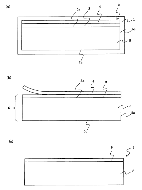
Figs. 1(a). 1(b) and 1(c) are diagrams schematically showing a
manufacturing process of a laminated sintered body 7 according to the first
and
second aspects of the present invention.
Figs. 2 (a) and 2(b) relate to another embodiment of the first and
second aspects of the present invention, in which green bodies 3A and 3B are
provided on both main faces of a green body 5 for a porous body and subjected
to
cold isostatic pressing to obtain a pressure molded body 6A.
Fig. 3 (a) shows a laminated sintered body 7 and a green body 10 for a
second electrode formed thereon.
Fig. 3 (b) shows a laminated sintered body 7 and a second electrode 11
formed thereon.
Fig. 4 is a front view schematically showing a conductive
interconnector 21 according to one embodiment of the third aspect of the
presentinvention.
Fig. 5 is a front view schematically showing one example of an
electrochemical cell 27.
Fig. 6 is a front view schematically showing a part of an
electrochemical cell 31 according to one embodiment of the third aspect of the
present invention.
Fig. 7(a) shows a pressure molded body 37 in a production example of
a sample according to the third aspect of the present invention.
Fig. 7(b) shows a sample of a conductive interconnector 41 according
to a comparative example.
Fig. 8 is a photograph taken by a microscope of a ceramic structure of
an electrochemical cell according to one embodiment of the first and second
11
CA 02461097 2004-03-22
04- 3-17;18:16 ;HOSODA&Partners Gowiings , # 16
FNGK0219PCT-CA
aspects of the present invention.
Fig. 9 is a photograph taken by a microscope of a ceramic structure of
an electrochemical cell according to one embodiment of a comparative example.
Fig. 10 is a schematic diagram for explaining a method of a
generation test.
BEST MODES FOR CARRYING OUT THE INVENTION
Figs. 1(a) to 1(c) show a production process of a laminated sintered
body according to one embodiment of the second aspect of the present
invention.
As shown in Fig. 1(a), a green body 3 for a dense body is laminated on a main
face 5a of a green body 5 for a dense body. Preferably, a resin sheet 4 is
laminated on and in direct contact with the green body 3 for dense body. 5b
represents a main face and 5c represents a side face of the green body 5. A
laminated body 2 is composed of the green body 5 for porous body, green body 3
for dense body and resin sheet 4. The laminated body 2 is covered with a film
1
over the whole surface and then subjected to cold isostatic pressing. It is
thus
possible to apply a uniform pressure over the whole surface of the laminated
body 2.
The :~1>un 1 is then peeled from the thus obtained pressure molded
body to obtain a laminated body shown in Fig. 1(b). The resin sheet 4 is
peeled
from the pressure molded body 6, which is then sintered to obtain a laminated
sintered body 7 shown in Fig. 1(c). The laminated sintered body 7 has a porous
body 8, and a dense body 9 laminated on the porous body 8.
According to the second aspect of the present invention, the green
body 5 for porous body and green body 3 for dense body are laminated and then
subjected to pressure molding by cold isostatic pressing to integrate them.
The
thus obtained pressured molded body 6 is then sintered. The green body 6 for
12
CA 02461097 2004-03-22
04- 3-17:18:16 ;HOSODA&Par2ners ~ GoW ings . # 17
FNOK0219PCT-CA
porous body has many open pores therein, so that substantial microscopic
irregularity is present on the suxface 5a of the green body 5 for porous body.
According to cold isostatic pressing, however, a pressure applied on the
surface
of the green body 3 for poxous body is substantially constant over the whole
surface of the green body 3. When the irregularity is present on the surface
5a
of the green body 5, the surface of the green body 3 is deformed
microscopically
along the irregularity so that the irregularity is transferred onto the
suxface of
the green body 3. The thickness of the green body 3 can be thus made
constant.
If the green body 3 for dense body is printed on the green body 5 for
porous body, air bubbles may be easily absorbed into the green body 3 during
the printing to result in many defects. Moreover, although the surface of the
green body 3 can be made flat, the surface of the underlying green body 5 has
irregularity in this case. The thickness of the green body 3 is inevitably
deviated locally. Such kinds of problems occur when uniaxial press molding
process is applied.
According to the second aspect of the present invention, the green
body 3 for dense body is thin, and a high pressure is applied over the whole
surface of the green body 3, so as to prevent the occurrence of air bubbles
due to
the printing or absorption of air. The pores and defects in the dense body can
be thus prevented.
Further, according to the second aspect of the present invention, the
thickness of the dense body 9 is made 25 ,u m or smaller and the thickness of
the porous body 8 is made 300 ,cc m or larger. The thin dense body is thus
provided on the thick porous body and subjected to cold isostatic pressing to
prevent the peeling of the green body fox dense body from the green body for
porous body due to a difference of thermal shrinkage during the sintering
13
CA 02461097 2004-03-22
04- 3-17:18:16 ;HOSODA&Partner5 Cowlings , ~ 18
FNGK0219PCT-CA
process of the green bodies.
In a field of an SOFC, a Japanese patent publication 8' 319181A
discloses a technique for producing a laminated sintered body of a separator
and
air electrode. According to the publication, a joining agent is applied
between
green bodies for separator and air electrode, which is laminated to obtain a
laminated and molded body. A predetermined number of through holes are
provided in the molded body. The outer surface of the molded body and the
inner wall surface facing the through holes are covered with a rubber
material.
The molded body is then subjected to cold isostatic pressing to obtain a
pressure
molded body, which is then sintered. According to the technique, the molded
body is pressed from the side of the inner wall surface facing the through
hole
by cold isostatic pressing to improve the adhesion of the separator and air
electrode and thus to prevent the peeling of them due to a difference of
thermal
shrinkage during the sintering. The technique is not for producing the dense
and thin film onto the thick and porous body as the present invention.
According to a preferred embodiment of the first and second aspects
of the present invention, the relative density of the dense body is 90 percent
or
higher, more preferably be 95 percent or higher and may be 100 percent at
maximum. Further in a preferred embodiment, the relative density of the
porous body is 90 percent or lower. The relative density of the porous body
may preferably be 40 percent or higher for improving the strength. Further in
a preferred embodiment, a difference between the relative densities of the
porous and dense bodies is 20 percent or more.
A thickness of 300 ,u m or more for the porous body is sufficiently
large for the purpose of the first and second aspects of the present
invention.
The thickness of the porous body may preferably be larger and more preferably
be 500 ,u m or larger. The upper limit of the thickness of the porous body is
14
CA 02461097 2004-03-22
04- 3-17;18:16 ~HOSODA&Par2ner5 Gowlm gs . # 19
FNGKQ219PCT-CA
not particularly defined and may be 5 mm or smaller for example. Although a
thickness of 25 ,u m or smaller for the dense body is sufficient for the
purpose
of the first and second aspects of the present invention, the thickness may
preferably be 15 ,u m or smaller. The thickness may preferably be 5 ,u m or
larger for preserving the air-tightness.
In a preferred embodiment, a resin sheet is laminated on the green
body for dense body and then subjected to cold isostatic pressing for press
molding. It is thus possible to prevent the adhesion of the green body 3 for
dense body onto the film 1 and thus to facilitate the removal of the pressure
molded body 6. Further, the resin sheet 4 has flexibility so that the sheet 4
does not prevent the above mechanism of making the thickness of the green
body 3 constant.
A material for the resin sheet is not particularly limited, and may
preferably be polyethylene terephthalate.
The thickness of the resin sheet is not particularly limited, and may
preferably be 200 ,u m or smaller for applying a pressure uniformly onto the
surface of the green body for dense body. On the other hand, if the resin
sheet
is broken, the thickness of the green body for dense body may be deviated. The
thickness of the resin sheet may preferably be 50 ,u m or larger fox
preventing
the above problems.
According to a preferred embodiment of the second aspect of the
present invention, the green body fox porous body and green body for dense
body
are subjected to cold isostatic pressing for pressure molding without
providing a
joining agent therebetween. It is possible to produce a strongly joined body
without the need of such joining agent according to the present invention.
Such joining agent present along the interface might be a cause for
introducing
pores and defects in the dense body depending on the materials used. It is
thus
CA 02461097 2004-03-22
04- 3-17;18:16 ;HOSO~A&Partners Gowiings . tf 20
FNGK0219PCT-CA
advantageous to prevent the use of the joining agent. The second aspect of the
present invention does not exclude embodiments using the joining agent.
According to a preferred embodiment of the second aspect of the
present invention, a plurality of green sheets for dense bodies are laminated
onto a manolayer of the green body for porous body, and then subjected to cold
isostatic pressing for press molding. For example, as shown in Figs. 2(a) and
2(b), green bodies 3A and 3B for dense bodies are laminated onto both main
faces 5a and 5b of the green body 5 for porous body, while resin sheets 4A and
4B are further laminated, respectively. The outer surfaces of the resin sheets
4A and 4B and side face 5c of the green body 5 are covered with the film 1,
and
then subjected to cold isostatic pressing. The resin sheets 4A and 4B are then
removed from the thus obtained pressure molded body to obtain a pressure
molded body 6A shown in Fig. 2(b).
After the pressure molded body 6A is obtained, the green body 5 for
porous body 5 is cut, as shown in a numeral 15, along a plane substantially
parallel with the main faces 5a and 5b to obtain two pressure molded bodies 6
(see Fig. 1(b)). The pressure molded bodies 6 are then sintered to obtain
laminated sintered bodies 7 shown in Fig. 1(c).
Alternatively, the pressure molded body 6A is sintered to obtain a
laminated sintered body having one porous body 8 and two dense bodies 9. The
laminated body is then cut to obtain two laminated sintered bodies 7 shown in
Fig. 1(c).
In a preferred embodiment, when the green bodies are subjected to
cold isostatic pressing, so called rubber press molding is applied (see "Fine
ceramics molding, processing and joining techniques" published by Kogyo
chosakai publishing Co. Ltd. 1989, pages 14 to 15). According to the
technique,
granule or powder is filled in a rubber mold and a pressure is applied onto
the
16
CA 02461097 2004-03-22
04- 3-17:18:16 ;HOS~DA&Partner5 Gowl~ngs , Ii 21
FNGK0219PCT-CA
rubber mold isostatically to press the granule or powder for molding. The
technique includes dry and wet processes.
The green body for porous body may preferably be a molded body
obtained by shaping a mixture of a main component for the porous body, an
organic binder and a pore-forming agent. The organic binder includes
polymethyl acrylate, nitxo cellulose, polyvinyl alcohol, polyvinylbutyral,
methyl
cellulose, ethyl cellulose, starch, wax, an acrylic polymer, a methacrylic
polymer,
and the like. The amount of the organic binder may preferably be 0.5 to b
weight parts, provided that the weight of the main component is 100 weight
parts.
The green body for dense body may preferably be a molded body
obtained by shaping a mixture of a main component for dense body, an organic
binder and a solvent (water or organic solvent). The organic binder may be
those described above. The amount of the organic binder may preferably be
0.5 to 20 weight parts, provided that the weight of the main component is 100
weight parts.
The green body for porous body may be shaped by any methods not
particularly limited, and may be a known ceramic molding process such as
doctor blade, dipping, extrusion, and metal mold pressing methods. The green
body for dense body may be shaped by any methods not particularly limited,
and may be a known ceramic molding process such as doctor blade, dipping and
extrusion methods. Since it is important to make the thickness of the green
body constant, doctor blade and extrusion methods are most preferred for
controlling the thickness in a specific range. When the green body is molded
by doctor blade method, a plasticizes such as polyethylene glycol,
polyalkylene
glycol, dibutyl phthalate and the like, and a defloculating agent such as
glycerin,
oleic acid, sorbitan triol or the like and a solvent such as toluene, ethanol,
17
CA 02461097 2004-03-22
04- 3-17:18:16 ;HOSODA&Pam ners Cowlings , q 22
FNGK0219PCT-CA
butanol or the like may preferably be used in addition to the above binder.
The thickness of the green body for dense body is not particularly
limited, as far as the thickness of the dense body after the sintering can be
controlled in a range of 25 ,u m or smaller.
Applications of the laminated sintered body according to the first and
second aspects are not particularly limited. The application may preferably be
a ceramic for use in electrochemical applications, particularly in an
electrochemical cell.
According to the first, second and third aspects of the present
invention, an electrochemical cell includes a solid oxide fuel cell, an oxygen
pump and a high temperature vapor electrolysis cell. The high temperature
vapor electrolysis cell can be used as a hydrogen production device, and also
as
a removing device of water vapor. In this case, the following reactions are
caused at the respective electrodes.
Anode: H20 + 2e -~ HZ +02-
Cathode: O 2 ~ 2e + 1/2 OZ
Further, the electrochemical cell can be used as a decomposition cell
for NOX andlor SOg. This Decomposition cell can be used as a purification
device for exhaust gas from motor vehicles, power generation devices or the
like.
In this case, oxygen in the exhaust gas is removed through a solid electrolyte
film while NOg is electrolyzed into nitrogen and oxygen, and the oxygen thus
produced by this decomposition can be also removed. Further, by this process,
vapor in the exhaust gas is electrolyzed to produce hydrogen and oxygen, and
the produced hydrogen reduces NOX to N2. Further, in a preferable
embodiment, the electrochemical cell is a solid oxide fuel cell.
In a particularly preferred embodiment, the laminated sintered body
of the first and second aspects is a laminated body of a solid electrolyte
film
18
CA 02461097 2004-03-22
04- 3-17:18:16 :HOSODA&Pa~2ners Gowl~ngs , ~ 23
FNGK0219PCT-CA
(dense body) and an electrode (porous body). The electrode may be an anode or
cathode.
The materials for a solid electrolyte layer may preferably be yttria-
stabilized zirconia or yttria partially-stabilized zirconia, and includes the
other
materials. In the case of NOX decomposition cell, cerium oxide is also
preferable.
The cathode material is preferably lanthanum-containing perovskite-
type complex oxide, more preferably lanthanum manganite or lanthanum
cobaltite, and most preferably lanthanum manganite. Into lanthanum
manganite, strontium, calcium, chromium, cobalt, iron, nickel, aluminum or the
like may be doped. Further, the cathode material may be palladium, platinum,
ruthenium, platinum-zirconia cermet, palladium-zirconia cermet, ruthenium-
zirconia cermet, platinum-cerium oxide cermet, palladium-cerium oxide cermet,
and ruthenium-cerium oxide cermet.
As the anode materials, nickel, palladium, platinum, nickel-zirconia
cermet, platinum-zirconia cermet, palladium-zirconia cermet, nickel- cerium
oxide cermet, platinum-cerium oxide cermet, palladium- cerium oxide cermet,
ruthenium, ruthenium-zirconia cermet and the like are preferable.
In a preferred embodiment, the laminated sintered body according to
the first and second aspects of the present invention may be a laminated body
of
an interconnector (dense body) and an electrode (porous body). The material
for the interconnector layer may preferably be a complex oxide of perovakite
type containing lanthanum and more preferably be lanthanum chromite. The
material for the porous body may be selected among the materials for anode and
cathode listed above.
When an electrochemical cell is produced, a molded body 10 for the
second electrode is provided on the surface of the solid electrolyte layer 9
of the
19
CA 02461097 2004-03-22
04- 3-17;18:16 ;HOSODA&Partners Cowlings , # 24
FNGKC219PCT-CA
laminted sintered body 7 as shown in Fig. 3 (a). The thus obtained molded
body 10 is sintered to form the second electrode 11 to obtain an
electrochemical
cell 12 as shown in Fig. 3(b).
When the laminated body is subjected to cold isostatic pressing, the
pressure may preferably be 500 kgflcm2 or higher and more preferably be 1000
kgflcm2 or higher, for improving the adhesion of the green bodies in the
laminated body. The upper limit of the pressure may be practically 10 tf/cm2.
When the pressure molded body is sintered, a dewaxing step may be
performed before the sintering step. It is also possible to complete the
dewaxing of the pressure molded body during a temperature ascending step for
the sintering. The sintering temperature may normally be 1200 to 1700
°C in
a pressure molded body for an electrochemical cell.
According to a preferred embodiment of the third aspect of the
present invention, one gas is an oxidizing gas and the other gas is a reducing
gas. In this case, the ceramic substrate is exposed to the oxidizing gas and
the
ceramic film is exposed to the xeducing gas. Many materials are known having
resistance against an oxidizing gas without resistance against a reducing gas.
The material for the ceramic substrate may be selected among a wide range of
known materials. A room for further reducing the internal resistance in the
ceramic substrate is thus large.
In a preferred embodiment of the third aspect of the present
invention, a conductive film is provided on the ceramic film to reduce the
contact resistance of the conductive interconnector and electrochemical cell.
In
this embodiment, however, the conductive film may preferably contacted with
the reducing gas. In this case, the ceramic substrate is exposed against the
oxidizing gas. The conductive film includes a metal foil and film.
The first gas and second gas may be reducing and oxidizing gases,
CA 02461097 2004-03-22
04- 3-17:18:16 ~HOSODA&Par2ners Cowlings , # 25
FNGK02t9PCT-CA
respectively. The first and second electrodes may be anode and cathode,
respectively.
The material having resistance against an oxidizing gas at an
operational temperature of the electrochemical cell means a material resistive
against oxidation and corrosion against the oxidizing gas. Such material
includes lanthanum manganite, lanthanum chromite and lanthanum cobaltite.
The material having resistance against a reducing gas at an
operational temperature of the electrochemical cell means a material resistive
against reduction and corrosion against the reducing gas. Such material
includes lanthanum chromite.
The material for the conductive film includes an electronic conductive
ceramic such as lanthanum manganite and lanthanum chromite, platinum,
silver, nickel, a nickel based alloy such as inconel and nichrome, and an iron
based alloy such as stainless steel.
The kinds of the oxidizing and reducing gases may differ depending
on the kind of the electrochemical cell for use. The materials for the ceramic
substrate and for ceramic film may be varied depending on the kind of the
electrochemical cell, and particularly depending on the kinds of the oxidizing
and reducing gases.
The oxidizing gas is not particularly limited, as fax as oxygen ions
may be supplied to a solid electrolyte film from the gas. The gas includes
air,
oxygen, NOg and SOR.
The reducing gas includes hydrogen, methane and carbon monooxide.
The thickness of the ceramic substrate is not particularly limited, and
may preferably be 0.3 mm or larger, and more preferably be 0.5 mm or larger,
for improving the structural strength of the conductive interconnector. The
thickness may preferably be 10 mm or smaller, and more preferably be 5 mm or
21
CA 02461097 2004-03-22
04- 3-17.18:16 :HOSODA&Partners Cowlings . # 26
FNGK02l9PCT-CA
smaller, for reducing the internal resistance in the ceramic substrate.
According to the third aspect of the present invention, the thickness
of the ceramic film is not particularly limited, as far as the air-tightness
can be
preserved against the first gas. If the first gas permeates through the
ceramic
film, the ceramic substrate may be deteriorated from the interface of the
substrate and film. The thickness of the ceramic film may preferably be 5 ,u m
or larger, and more preferably be 10 ,u m or larger, for improving the air-
tightness of the ceramic film. Further, the thickness of the ceramic film may
preferably be 50 ,c.C m or smaller, and more preferably be 25 ,u. m or
smaller,
for reducing the internal resistance in the ceramic film.
Fig. 4 is a front view schematically showing a conductive
interconnector 21 according to one embodiment of the third aspect of the
present invention. Fig. 5 is a front view schematically showing an
electrochemical cell 27, and Fig. 6 is a front view showing essential parts of
an
electrochemical device 31 having a plurality of conductive interconnectors 21
and electrochemical cells 27.
As shown in Fig. 4, the conductive interconnector 21 has a ceramic
conductor 22 and a conductive film 25. In the present example, the ceramic
substrate 23 is exposed to the oxidizing gas, and the ceramic film 24 is
exposed
to the reducing gas. In a preferred embodiment, one ceramic substrate 23
made of lanthanum manganite and ceramic film 24 made of lanthanum
chromite are molded as an integrated body by cold isostatic pressing and then
sintered. The ceramic substrate 23 has a plate-shaped main part 23c, and a
plurality of elongate protrusions 23a protruding from the main part 23c. A
plurality of elongate grooves 26 each having a cross sectional shape of a
rectangle are formed in the ceramic substrate 23. The adjacent grooves 26 are
defined by the protrusions 23a. 23b repxesent the surface of protrusion 23a. A
22
CA 02461097 2004-03-22
04- 3-17:18:56 ;HOSODA&Partners Cowlings , # 27
FNGK0219PCT-CA
ceramic film 24 is formed on the main face 23d of the ceramic substrate 23.
The conductive film 25 is provided on the film 24.
As shown in Fig. 5, the electrochemical cell 27 of the present example
has a first electrode 30, a solid electrolyte film 33 and a second electrode
28. In
a preferred embodiment, the second electrode 28 and solid electrolyte film 33
i are shaped as an integrated body by cold isostatic pressing and then
sintered.
The second electrode 28 has a plate-shaped main part 28c, and a plurality of
1 otrusion 28a rotrudin fro the main art 2
a ongate pr s p g m p 8c. The adjacent
j protrusions 28a axe defined by the groove 29. 28b represents the surface of
the
protrusion 28a.
As shown in Fig. 6, a plurality of the electrochemical cells 27 and
conductive interconnectors 21 are laminated in turns to produce a stack. In
this case, the surface 23b of the ceramic substrate 23 an the groove side is
opposed to and electrically connected with the electrode 30. The face of
protrusion 28b of the electrode 28 is electrically connected with the
conductive
film 25 of the conductive interconnector 21. The groove 26 may function as a
flow route for the oxidizing gas, and the groove 29 may function as a flow
route
for the reducing gas. Further, only two electrochemical cells 27 and two
conductive interconnectors 21 are shown in Fig. 6, additional electrochemical
cells and conductive interconnectors may be arrange on the upper and lower
sides of the stack shown in Fig. 6.
The conductive interconnectvr 21, particularly ceramic conductor 22,
may be made by any process not particularly limited, including the following
methods.
(1) The ceramic substrate and film are sintered separately and then
joined with each other using an inorganic adhesive.
(2) After the ceramic substrate is produced by sintering, the ceramic
23
CA 02461097 2004-03-22
04- 3-17;18:16 ;HOSODA&Partners Cowlings . # 28
FNGR0219PCT-CA
film is directly formed on the surface of the substrate. The film may be
formed
by wet and dry processes. In the case of the wet process, a ceramic slurry is
applied on the surface by an application method such as dipping and spin
coating and the thus formed film is then sintered. The dry process includes
sputtering, chemical vapor deposition, physical vapor deposition, metal
organic
chemical vapor deposition and vapor deposition.
(3) Green bodies for the ceramic substrate and ceramic film are
laminated and then sintered.
According to the third aspect of the present invention, the green
bodies for ceramic substrate and ceramic film may preferably be green bodies
obtained by shaping a mixture of ceramic powder, an organic binder and a
solvent (optionally used). The organic binder includes polymethyl acrylate,
vitro cellulose; polyvinyl alcohol, polyvinylbutyral, methyl cellulose, ethyl
cellulose, starch, wax, an acrylic polymer, a methacrylic polymer, and the
like.
The amount of the organic binder may preferably be 0.5 to 20 weight parts,
provided that the weight of the main component is 100 weight parts.
The ceramic conductor may be used as a conductive interconnector.
When the conductive film 25 is joined with the ceramic conductor 22 as
described above, a conductive adhesive may preferably be used for the
adhesion.
The conductive adhesive includes nickel paste. Further, the conductive film 25
may be formed with nickel plating.
EXAMPLES
(Experiment "A" according to the second aspect of the present invention)
(Production of a pressure molded body 6)
Alumina balls each having a diameter of 10 mm were contained in a
container of nylon. 100 weight parts of 3 mole percent yttria stabilized
zirconia,
24
CA 02461097 2004-03-22
04- 3-17;18:16 :HOSODA&Par2ners Cowlings . .
FNOK0219PCT-CA
20 weight parts of toluene, 11 weight parts of ethanol and 2 weight parts of
butanol as solvents were added and mixed in a ball mill at a revolution speed
of
60 rpm. After that, 8 weight parts of polyvinylbutyral, 3 weight parts of
dibutyl phthalate, 26 weight parts of toluene and 15 weight parts of ethanol
were added to the mixture, and further mixed in the ball mill. The thus
obtained slurry was shaped as a sheet by doctor blade method on a sheet
(thickness of 100 ,u m: resin sheet ~ of polyethylene terephthalate. The green
sheet 3 for dense body having a width of 50 mm and thickness of 20 ,u m of 3
mole pexcent yttria stabilized zirconia (for a solid electrolyte film) was
produced
on the resin sheet 4.
Further, an organic binder and watex were added to nickel oxide
powder and 8 mole percent yttxia stabilized zirconia powder, and then wet
mixed in a ball mill to obtain a mixture, which was dried and granulated. The
granulated powder was shaped in a metal mold to produce a green body 5
having a thickness of 3 mm (green body for fuel electrode).
The above obtained green body 3 for dense body and resin sheet 4
were laminated on the green body 5 so that the green bodies 3 and 5 contact
each other. The thus obtained laminated body were covered with a contained
of a film for vacuum packaging and subjected to cold isostatic pressing. (at a
pressure of 2 ton/cm2 and a holding time of 1 minute). The thus obtained
pressure molded body was removed from a mold and the resin film 4 was
removed to obtain a pressure molded body 6.
(Sintering of the pressure molded body 6)
The pressure molded body was sintered in air at a maximum
temperature of 1400 °C for 2 hours to obtain a laminated sintered body
7.
(Production of air electrode)
100 weight parts of lanthanum manganite powder having an average
CA 02461097 2004-03-22
04- 3-17:18:16 ;HOSODA&Partners Cowlings , # 30
FP7GK0219PCT-CA
diameter of 3 ,u m, 3 weight parts of polyvinyl alcohol modified with alkyl
acetate, and 30 weight parts of terepineol were mixed in an alumina pot to
produce paste. The thus obtained paste was applied using a screen printing
system to from a layer 10 shown in Fig. 3(a). The layer 10 was dried and
sintexed at a maximum temperature of 1250 °C for 1 hour to form an air
electrode.
The thus obtained laminated sintered body 7 was observed at the
polished surface using a scanning electron microscope (at a magnitude of 500),
and the results were shown in Fig. 8. In Fig. 8, the fuel electrode $ was
shown
in the lower side and the solid electrolyte film 9 was shown in the upper
side.
Pores and defects were not observed in the solid electrolyte film and the film
thickness proved to be constant.
Fig. 9 shows a photograph taken by a scanning electron microscope
(at a magnitude of 500) of the laminated sintered body whose solid electrolyte
film 9 was formed by absorption dipping. As shown in Fig. 9, the fuel
electrode
$ was shown in the lower side and the solid electrolyte film 9 was shown in
the
upper side. Micro pores and defects were observed in the solid electrolyte
film.
(Experiment "B" according to the second aspect of the present invention)
Laminated sintered bodies of examples shown in tables 1 and 2 wexe
produced according to the same procedure as the experiment "A". The width of
the molded body was 150 mm and the thickness of the molded body was
variously changed. Further, samples having diameters of ~ 90 mm (area of
63.6 cm2), ~ 50 mm (area of 19.6 cm2) and ~ 16 mm (area of 2.0 cm2) wexe
cut out from the laminated sintered bodies for measurement.
The helium leakage rate was measured by vacuum spraying method
using a helium leakage detector (a mass analysis type helium leakage detector
26
CA 02461097 2004-03-22
04- 3-17;18:16 ;HOSODA&Parcners Cowlings . ~ 31
FN~K0219PCT-CA
"MSE-11FA" supplied by Shimadzu) for each of the laminated sintered bodies of
the examples. Each of the laminated sintered bodies was used to produce an
SOFC according to the same procedure as the experiment "A". The initial
generation output was measured for each SOFC. Specifically, the laminated
sintered body was set in a system for testing generation. Platinum meshes
were provided on the air and fuel electrodes, respectively, for collecting
electric
current. Air was flown in the side of the air electrode in a flow rate of 500
cc/min, and nitrogen was flown in the side of the fuel electrode in a flow
rate of
500 cc/min, while the temperature was elevated. The temperature was then
held at 800 °C and hydrogen was flown in the side of the fuel electrode
in a flow
rate of 500 cc/min to replace the nitrogen gas. After the atmosphere was
stabilized, a voltage of 0.7 volt was applied and the output (initial output)
was
measured 10 hours later.
After that, an initiation and termination cycle test was performed.
Specifically, after the initial output was measured, (1) current was
terminated,
and nitrogen was flown in the side of the fuel electrode at a flow rate of 500
cc/min for 14 hours, while the temperature was maintained at 800 °C.
After
that, (2) hydrogen was flown in the side of the fuel electrode at a flow rate
of 500
cc/min to replace the gas. After the atmosphere was stabilized, a voltage of
0.7
volt was applied for 10 hours. The above steps (1) and {2) were repeated 10
times in each initiation and termination cycle test. The output after one
initiation and termination cycle test was measured, and the results were shown
in the following tables.
27
CA 02461097 2004-03-22
04- 3-17:18:16 :HOSODA&Partners Cowlings . # 32
FNGK0219PCT-CA
Table 1
ComparativeComparativexample TempleExampl
3
xample ple 1 2
1 2
ess of pornus 10 0 10 0 3 0 1 0 1 0
body 0 0 0
0 0
(lxm)
'ckness of dense 5 0 5 0 2 5 1 0 1 0
body
(l,~m)
a of solid electrolyte2 6 3. 6 3. 2 1 9
part 6 6 .
6
of cell
( c m2/single
cell)
Possibility of possibleimpossiblepossiblepossiblepossible
production of
Laminated sintered
body
Helium, leakage 0 . - 0 . 0 . 0 .
rate 0 0 0 0 0 0
2 1 0 3
2
( X 10-s Pa ~ or lower
mg/s)
Generation test
Initial output 0. 1 - 0 . 0 . 0.
6 2 4 3
6
(W/cmz)
Output after initiation
and termination - - 0. 2 - -
cycle test
(W/cm2)
28
CA 02461097 2004-03-22
D4- 3-17:18:16 ;HOSODA&Partners Cowlings , k 33
FNGK0219PCT-CA
~2
xampleExampleExampleComparativeComparative
4 5 6 ~ xamplexample
3 4
Thickness of
porous body
(um) 1000 1000 300 1000 1000
Thickness of
dense body
(gym) 10 10 5 60 20
ea of solid electrolyte
art of cell 6 3. 1 1 6 3 2 6 3.
6 3 . 6
6
( c m2/ single
cell)
Possibility of possibleosaibIepossiblepossiblepossible
production
of laminated
sintered body
Helium leakage 0 . 0 . 0 . 0 . 1. 5
rate 0 2 9 3 6
8 5
(x 1 0-6 Pa
mils)
Generation test
Initial output 0 . 0 . 0 . 0 . 0 . 3
(W/c m2) 3 3 3 1 1
5 5
Output after 0 , 0 . 1
initiation an 3 6
5
termination cycle
teat
(W/cm2)
As can be seen from the results, the output after the initiation and
termination cycle test can be maintained at a high value according to the
second
aspect of the present invention.
(Experiment "C" according to the third aspect of the present invention
(Production of a conductive interconnector)
Aluiuina balls each having a diameter of I0 mm were contained in a
container of nylon. 100 weight parts of lanthanum chromite powder, 20 weight
29
CA 02461097 2004-03-22
04- 3-17:18:16 :NOSODA&Partners Gowling5 . # 34
FNGK0219PCT-CA
parts of toluene, 10 weight parts of ethanol and 2 weight parts of butanol
were
added as solvents and mixed in a ball mill at a revolution speed of 60 rpm.
After that, 8 weight parts of palyvinylbutyral, 3 weight parts of dibutyl
phthalate, 27 weight parts of toluene and 15 weight parts of ethanol were
added
to the mixture, and further mixed in the ball mill. The thus obtained sluxry
was shaped as a sheet by doctor blade method to produce a green sheet 35
having a width of 50 mm and thickness of 20,tt m of lanthanum chromite (see
Fig. 7(a): green body for interconnector).
Further, 3 weight parts of an organic binder and water were added to
100 weight parts of lanthanum manganite powder, and then wet mixed in a ball
mill to obtain a mixture. The mixture was dried with a spray drier and
granulated. The granulated powder was shaped in a metal mold for pressure
molding to produce a green body 34 having a thickness of 6 mm. The green
body 34 and green sheet 35 were laminated and a film 36 made of polyethylene
terephthalate (having a thickness of 100 ,CC m) was laminated on the green
sheet 35. The laminated body was contained in and covered with a container of
a film for vacuum packaging, and then subjected to cold isostatic pressing tat
a
pressure of 2 ton/cm2 and a holding time of 1 minute). The thus obtained
pressure molded body was removed from the container, and the film container
was peeled off to obtain a pressure molded body 37.
The pressure molded body 37 was sintered in air at a maximum
temperature of 1600 °C for 2 hours to obtain a laminated sintered body
27.
The side of lanthanum manganite was processed by grinding to form grooves
each having a width of 3 mm and depth of 3 mm to obtain a ceramic conductor
22 having a length of 50 mm, a width of 50 mm and thickness of 5 mm. A
conductive film 25 of nickel was then formed on the ceramic conductor 22 by
electroless plating to obtain a conductive interconnector 21.
CA 02461097 2004-03-22
04- 3-17:18:16 ;NOSODA$Partners Gowling5 . N 35
FNGK0219PCT-CA
(Production of a conductive interconnector according to a comparative example)
3 weight parts of an organic binder and water were added to 100
weight parts of lanthanum chromite powder, and then wet mixed in a ball mill
to obtain a mixture. The mixture was dried with a spray drier and granulated.
The granulated powder was shaped in a metal mold for pressure molding to
produce a green body having a thickness of 6 mm. The green body was
contained in and covered with a container of a film fox vacuum packaging, and
then subjected to cold isostatic pressing (at a pressure of 2 ton/cm2 and
holding
time of 1 minute). The thus obtained pressure molded body was removed from
the container, and the film container was peeled off to obtain a pressure
molded
body. The pressure molded body was sintered in air at a maximum
temperature of 1600 °C for 2 hours to obtain a laminated sintered body.
The
sintered body was processed by grinding to form grooves each having a width of
3 mm and a depth of 3 mm to obtain a ceramic conductor 40 (see Fig. 7(b))
having a length of 50 mm, a width of 50 mm and thickness of 5 mm. A
conductive film 25 of nickel was then formed on the ceramic conductor 40 by
electroless plating to obtain a conductive interconnector 41.
(Production of cell for solid oxide fuel cell)
(Production of substrate functioning as fuel electrode)
An organic binder and water were added to nickel oxide powder and 8
mole percent yttria stabilized zirconia powder, and then wet mixed in a ball
mill
to obtain a mixture. The mixture was then dried and granulated. The
granulated powder was press molded in a metal mold to produce a green body
having a length of '70 mm, width of 70 mm and thickness of 3 mm (green body
for fuel cell.). The molded body was sintered at 1400 °C for 2 hours.
The
sintered body was then processed by grinding to form grooves each having a
width of 3 mm and depth of 3 mm to obtain a substrate functioning as a fuel
31
CA 02461097 2004-03-22
04- 3-17;18:16 :HOSODA&Partners Cowlings , ,p 36
FNGK0219PCT-CA
electrode having a length of 50 mm, width of 50 mm and thickness of 5 mm.
(Production of solid electrolyte film)
$ mole percent yttria stabilized zirconia powder for spray drying
having an average diameter of 20 ,u m was supplied into plasma flame of an
output of 40 kW to form a solid electrolyte film having a thickness of 50 ,u m
by
plasma spraying on the substrate functioning as fuel electrode. After that,
the
solid electrolyte film was heat treated at 1350 °C for 2 hours for
densifying the
film.
(Production of air electrode)
100 weight parts of lanthanum manganite powder having an average
diameter of 3 ,u m, 3 weight parts of polyvinyl alcohol modified with alkyl
acetate, and 30 weight parts of terepineol were mixed in an alumina pot to
produce paste. The thus obtained paste was applied using a screen printing
system to from a layer having a length of 40 mm, width of 40 mm and thickness
of 30 ,u m shown in Fig. 3(a). The layer 10 was dried and sintered at a
maximum temperature of 1250 °C for 1 hour to form an air electrode.
(Generation test)
The conductive interconnector and solid electrolyte fuel cell were
assembled to provide a stack shown in Fig. 10. The stack was set in an
electric
furnace, and pressed vertically as arrows "A". Argon gas was flown in the
reduction side and air was flown in the oxidation side, while the temperature
was elevated to 1000°C. After the temperature reached 1000°C,
argon gas was
replaced with hydrogen gas in the reduction side. The current and voltage
property was measured, while the flow rates of air and hydrogen were adjusted
at 1 liter/min and x liter/min, respectively. An output of 0.1 W/cm2 was
obtained at the maximum. Fracture and corrosion were not observed in the
conductive interconnector 21 to prove that the assemble was stable. Further,
32
CA 02461097 2004-03-22
04- 3-17;18:16 ;HOSODA&Par2ners Cowlings . !l 37
FNGK0219PCT-CA
the above measurement was carried out except that the conductive
interconnector 21 was replaced with the conductive interconnector 41 of the
compaxative example. It was proved that the maximum output was
considerably reduced to 0.05 W/cm2.
33