Note: Descriptions are shown in the official language in which they were submitted.
CA 02461169 2004-03-22
1
DESCRIPTION
Laser Beam Irradiation Device
Technical Field
The present invention relates to a laser beam irradiation device for
projecting a
laser beam to one's skin for beauty treatments such as skin treatment, removal
of
undesired hair and suchlike to make persons more beautiful.
Background Art
When human skin is exposed to a laser beam under the skin temperature of 36
centigrade, on the skin caused is a certain vital reaction, which is called
"non-thermal
reaction". It includes photoelectric effect, photo-magneto effect, photo-
dynamics effect,
photochemical effect, photo-immunization effect, photo-zymogenesis effect and
other
such like optical effects.
Such non-thermal reactions are applied to body treatments such as slimming and
hair restoration, since they stimulate blood circulation, body metabolism and
the likes.
Also, when the skin is exposed to a laser beam, Joule heat is caused in the
skin
tissue by photothermal reaction to raise the temperature of the skin tissue.
The rise of the skin temperature causes various reactions such as; flashing,
protein transformation, blood clot, vaporization, and carbonisation.
Such photothermal reactions are applied to beauty treatments such as: a skin
beauty treatment, in which birth marks, stains, freckles and other unpleasing
pigment cells
are reduced into minute particles almost unnoticeable; and a depilation
treatment, in
which protein transformation is caused in hair root cells to destroy the
regeneration
mechanism of human hair.
These non-thermal and photothermal reactions can be selectively caused,
depending on how much energy density a used laser beam has.
Referring to Fig.7, a semiconductor laser diode is responsive to application
of
voltage for starting an electric current to flow, and at the outset it
radiates natural light.
A laser oscillation is caused when the so started electric current rises
beyond a certain
threshold value, and the laser output drastically increases in proportion to
the increasing
electric current, and accordingly the energy density of the laser beam
increases.
The object of the present invention is to provide a laser beam irradiation
device
capable of giving both the non-thermal and photothermal treatments by
controlling the
amount of electric current excited in its semiconductor laser diode to adjust
output power
CA 02461169 2004-03-22
2
of the laser beam.
Disclosure of Invention
To attain this object a laser beam irradiation device according to the present
invention, specifically as defined in claim 1 comprises:
a semiconductor laser diode for producing a laser beam;
a switching means for changing the semiconductor laser diode in operation from
one to another outputting state or vice versa; and
a control circuit for controlling the amount of working current flowing in the
semiconductor laser diode to adjust output power of the laser beam by using
the switching
means for an appropriate performance of either non-thermal or photothermal
treatments.
The laser beam irradiation device according to claim 2 is a device as defined
in
claim 1, whose switching means is adapted to change the semiconductor laser
diode
between high-outputting state and low-outputting state.
The laser beam irradiation device according to claim 3 is a device as defined
in
claim l, whose control circuit functions to make the working electric current
flows and
stops in the semiconductor laser diode at regular intervals, thereby
projecting the laser
beam intermittently.
The laser beam irradiation device according to claim 4 is a device as defined
in
claim 3, of which one shot of the intermittent radiation can be controlled in
terms of
rotation angle of a rotary control.
Brief Description of Drawings
Fig.l is a perspective view of a laser beam irradiation device according to
the
present invention;
Fig.2 is a front view of the console panel of the laser beam irradiation
device;
Fig.3 is a front view of the hand-held applicator;
Fig.4 is a side view of the hand-held applicator, partly in section;
Fig.S is a block diagram of the control circuit;
Fig.6 is a block diagram of the drive circuit; and
Fig.7 is an excitation current-versus-laser output graph.
Best Mode for Carrying Out the Invention
The present invention is described below in respect of preferred embodiments.
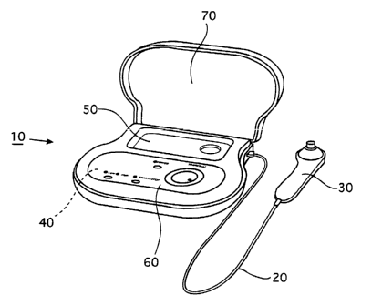
Fig.l shows how it looks in appearance.
CA 02461169 2004-03-22
3
The laser beam irradiation device comprises a major body 10 and an associated
hand-held applicator 30 connected to the major body 10 via a given length of
cable 20.
The major body 10 contains a control circuit 40, and the housing of the major
body 10 has a recessed compartment 50 for accommodating the hand-held
applicator 30
and a console 60 on its top surface, and a lid 70 hinged to one side of the
housing.
Fig.2 shows the console.
On the console 60 arranged are a power switch S1, an output-power switching
unit S2, a standby switch S3 and a rotary radiation control V 1, and further
arranged are a
power indicator LED Ll next to the power switch S 1, a low-power indicator LED
L21 and
a high-power indicator LED L22 next to the output-power switching unit, and a
standby
indicator LED L3 next to the standby switch S3.
The power switch S 1 functions to turn the power supply on and off (or put in
or
out of circuit), and accordingly the power indicator lamp L1 turns on and
offrespectively.
The output-power switching unit S2 functions to make the laser change in
operation from a relatively low outputting state (for example 1.0 watt) to a
relatively high
outputting state (for example 1.6 watts) or vice versa.
Then, the low power indicator LED L21 turns on for the relatively low
outputting state and turns off for the relatively high outputting state,
whereas the
high-power indicator LED L22 turns off for the relatively low outputting state
and turns
on for the relatively high outputting state.
The output-power switching unit S2 can work only when the standby switch S3
is off.
The initial output power of the laser beam is automatically set at the
relatively
low outputting state Lo in response to the turning-on of the power switch S 1.
When the standby switch S3 is turned on, the laser is set on a standby
condition
for radiation and the standby indicator LED L3 turns on. When the standby
switch S3 is
turned off, the standby condition of the laser is cancelled and the standby
indicator LED
L3 turns off.
The mere switching-on of the power switch S 1 keeps the laser stay in
non-standby condition.
When the standby switch S3 is turned on, an associated timer starts counting
to
automatically turn off the standby switch S3 after a predetermined period (for
example,
20 minutes) has passed irrespective of whether or not the laser has been
radiated.
The rotary radiation control V 1 is used to set a duration or dose of a single
shot
in the intermittent radiation in terms of its rotation angle, and the duration
can change for
CA 02461169 2004-03-22
4
example from one to nine seconds.
The rotary radiation control V 1 can be operated to set a desired duration of
each
shot even if the standby switch S3 is on. The initial radiation dose when the
power
switch S 1 is turned on is determined by the rotation angle of the rotary
radiation control
V l .The shot-to-shot interval in the intermittent radiation is determined
(for example, 1.5
seconds) beforehand.
Referring to Figs.3 and 4, the hand-held applicator 30 has a face H projecting
laterally from its top, and a push button switch S4 on its side.
Also, the hand-held applicator has vent holes "a" and "b" at the lower part
and
on the rear side of the face H.
The face H has a spherical lens 31 press-fitted in its center hole, and the
face H
has a hollow cylinder 32 integrally connected to its circumference, encircling
the
spherical lens 31. The hand-held applicator 30 is applied to one's skin by the
hollow
cylinder 32 at its edge.
A coaxial cylindrical electrode 33 is embedded in the hollow cylinder 32 to
project forward therefrom at its open edge.
A heat sink 34 is placed behind the spherical lens 31, and a semiconductor
laser
diode 35 is press-fitted in a through-hole bored in the center of the heat
sink 34.
A cooling fan 36 is placed behind the heat sink 34.
The laser beam from the semiconductor laser diode 35 focuses on the focal
point
of the spherical lens 31 in the focal plane, in which the opening of the
hollow cylinder 32
lies. The focal length of the spherical lens 31 is short enough to converge
all the light
energy to a limited spot, allowing the so converged beam to diverge beyond the
focal
point with the result that the light energy is distributed over the extensive
area.
Accordingly the light energy density drastically decreases with the distance
from
the focal point, and therefore, there is little or no fear of injuring a
living body even if it is
exposed to the so dispersed light beam.
The heat sink 34 allows the heat generated by the semiconductor laser diode 35
to transmit therethrough. Thus, the semiconductor laser diode 35 is prevented
from
lowering its output.
The heat sink 34 is made of aluminum or aluminum alloy, whose thermal
conduction is relatively high, and the heat sink 34 has further through holes
made therein
to effectively improve its heat radiation.
The semiconductor laser diode 35 may be a PN junction diode of GaAs or any
other compound semiconductor, which can be excited by making an electric
current flow
CA 02461169 2004-03-22
therethrough for laser oscillation.
The peak-to-peak wavelength of the semiconductor laser diode is 600 to 1600
nm long, and the laser output ranged from SmW to 3W, thereby efficiently
causing a
sufficient photothermal reaction on the skin.
Further caused are additional optical efFects other than the required
photothennal
reaction, such as photoelectric effect, photo-magneto effect, photo-dynamics
effect,
photochemical effect, photo-immunizing effect, photo-zymogenesis effect and
the like.
The photo-biological activation expedites the body's metabolism and blood
circulation
under the skin. The laser beam is hardly absorbed by the water contents and
blood, and
therefore, it can reach deep under the skin.
Fig.S shows the control circuit of the laser beam irradiation device.
It comprises: a CPU 41 having a memory 42 and a timer circuit 43 both built
therein; an output-power switching unit S2, a standby switch S3, a push button
switch S4,
a rotation angle detector 45 for determining the instantaneous rotation angle
of the rotary
radiation control V 1, and a touch sensor circuit 46 for detecting the
touching of the
electrode 33 on the skin, all of which are connected on the input side of an
I/O port 44;
and a drive circuit 47 connected on the output side of the I/O port 44 for
controlling the
working current in the semiconductor laser diode 35.
The touch sensor circuit 46 comprises a high-frequency oscillator circuit and
a
switching circuit responsive to the working or non-working of the oscillator
for turning on
or off.
The electrode 33 is connected to one terminal of an oscillation coil of the
oscillator circuit, and the oscillation stops as the electrode 33 touches the
skin. The
switching circuit is responsive to the stop of the oscillation for turning
off.
The touch sensor circuit 46 may include an impedance element such as a
capacitance or a resistance whose impedance drastically varies in response to
the touching
of the electrode to the skin, or may include a switching element or a
piezoelectric element
responsive to the touching of the electrode to the skin.
Fig.6 shows a block diagram of the drive circuit 47.
The CPU 41 is responsive to the switching-on and -off of the output-power
switching unit 52 for sending a reference signal to an amplifier 472 via the
I/O port 44
and a D/A converter 471, so that the amplifier 472 provides at its output
terminal a
reference voltage, with respect to which a control reference voltage for a
desired laser
output is determined.
The semiconductor laser diode 35 radiates the laser beam from its opposite
sides,
CA 02461169 2004-03-22
6
and a photo-diode 473 receives one of the opposite laser beams to provide a
light-accepting voltage at its output terminals. The so acquired light-
accepting voltage is
directed to the amplifier 474 for amplification, thereby obtaining the monitor
voltage.
The reference voltage and the monitor voltage are applied to a differential
amplifier 475, and a differential voltage is amplified by an amplifier 476.
Thus a
controlled working electric current is made to flow in the semiconductor laser
diode 35 so
that it may be energized and oscillated at the set output level.
The semiconductor laser diode can be thus switched to the relatively high- or
low- powered oscillation Lo or Hi.
The CPU 41 carries out the on-and-off control of the working current from the
drive circuit 47 under the control of the timer circuit 43.
The timer control includes two different modes, that is, the treatment time
control in which the working current is made to flow a predetermined length of
time for
each treatment, and the radiation dose control in which the working current is
made to
flow a predetermine length of time for each shot in the intermittent
radiation.
The duration of a single shot in the intermittent radiation can be set terms
of the
rotation angle of the rotary radiation control V 1.
In carrying out a required beauty treatment with the so constructed laser beam
irradiation device of the present invention, first the power switch S 1 is
turned on.
Then, the output-power switching unit S2 is turned on to select either the
relatively low outputting state Lo for the non-thermal treatment or the
relatively high
outputting state Hi for the photothermal treatment.
Next, the rotary radiation control V 1 is rotated to set the duration of a
single shot
in the intermittent radiation.
Next, the standby switch S3 turns on to put the device in the standby
condition.
The hand-held applicator 30 is held in hand with the face H directed towards a
selected spot on the skin at the angle of 90 degrees relative to the skin, and
then, the
electrode 33 of the cylinder 32 is pushed against the selected spot.
Then, the push button switch S4 is depressed to turn the semiconductor laser
diode 35 on for predetermined seconds, and then turns off for prescribed
seconds.
The semiconductor laser diode 35 turns on or off alternately, projecting onto
the
spot the laser beam of the required strength Lo or Hi, which is selected by
the
output-power switching unit S2.
A required beauty treatment is repeated as many times as required while moving
the electrode 33 of the hand-held applicator 30 from place to place on the
skin.
CA 02461169 2004-03-22
7
The radiation of the laser beam is made to stop in response to the electrode
33
being taken off from the skin, and the radiation of the laser beam is made to
start in
response to the electrode 33 being put on the skin.
Assuming that a fixed length of time has passed since the turning-on of the
standby switch S3, it automatically turns off, thereby stopping the radiation
of the laser
beam.
Industrial Applicability
As described above, the laser beam irradiation device of the present invention
is
responsive to the selection of the beauty treatment modes for appropriately
increasing or
decreasing the working electric current in the semiconductor laser diode. For
that
purpose, the output-power switching unit is designed to be selectively turned
toward
relatively high outputting state for photothermal treatment and toward
relatively low
outputting state for non-thermal treatment. This arrangement permits a safe
and efficient
beauty treatment as well as an expansion of the applicable scope of the laser
beam
irradiation device.
Radiation of the laser beam is intermitted at a fixed interval by controlling
the
working electric current in the semiconductor laser diode.
The shot duration of the laser beam can be controlled in terms of the rotation
angle of the rotary radiation control.
In addition to the controlling of the power output of the laser, the energy
density
can be finely controlled in terms of the duration of beam radiation. This
arrangement
facilitates the sophisticated control of the laser output to meet a variety of
beauty
treatments as required.
The use of the rotary radiation control facilitates the controlling of the
radiation
of the laser beam.
CA 02461169 2004-03-22
AMENDMENT (According to Article 11 )
To: Mr. Commissioner of the Patent Office
1 Identification of the International Application
PCT/JP02/09293
2 Applicant
Name: YAMAN LTD.
Address: 4-4, Furuishiba 1-chome, Koto-ku, Tokyo, 135-0045, JAPAN
Nationality: Japan
Residence: Japan
3 Agent
Name: (7777) Patent Attorney MAKI, Teturo
Address: Suite 402, Shuwa Kioicho Park Bldg.
3-6, Kioi-cho, Chiyoda-ku, Tokyo, 102-0094, JAPAN
4 Item to be Amended
Specification and Claims
5 Contents of Amendment
( 1 ) Page 2 is amended as attached.
(2) Claim 1 is amended as attached.
6 List ofAttached Documents
(1) Substitute page 1 one copy
(2) Substitute page 8 (amended claims) one copy