Note: Descriptions are shown in the official language in which they were submitted.
CA 02461540 2004-03-23
WO 03/032492 PCT/EP02/11075
A Reconficturable Integrated Circuit With A Scalable Architecture
BACKGROUND OF THE INVENTION
1. Field of the Invention
The present invention relates to the field of integrated circuit (IC). More
specifically, the present invention relates to the architecture of
reconfigurable
ICs.
2. Background Information
The art of design and manufacturing ICs is generally known. Over the
years, as the technology of designing and manufacturing ICs continues to
improve, increasing number of electronic elements are being packed into a
single IC, and the interrelationship between these elements are increasingly
complex. With increased density and complexity, the cost for making an IC
manufacturing mask has increased substantially correspondingly.
Between different offerings of a modern IC product family, or between
successive offerings, often times the functionalities are different only in a
relatively small incremental way, when viewed in the context of the totality
of its
logic. Thus, in view of the high cost of a new IC mask as well as other
factors,
increasingly IC designers desire to have ICs that are partially reconfigurable
to
accommodate the small incremental changes in functionalities between the
different offerings.
U.S. Patent 5,574,388 discloses a reconfigurable IC designed for
emulation application. The architecture including in particular the integrated
debugging facilities was particularly suitable for the intended use. However,
general purpose partially reconfigurable integrated circuits present a
different
set of challenges. One desirable attribute is scalability to provide more
flexible
tradeoffs between area consumption versus routability.
Thus, an improved reconfigurable IC architecture is desired.
SUMMARY OF THE INVENTION
An integrated circuit (IC) includes a number of function blocks, of which
at least one is a reconfigurable function block. Each function block may be a
reconfigurable function, a non-reconfigurable function or recursively expanded
1
CA 02461540 2004-03-23
WO 03/032492 PCT/EP02/11075
with additional "nested" function blocks interconnected with the same
architecture. The IC further includes a number of external input pins, and a
number of external output pins.
The elements, at least at the IC level, are coupled in a manner such that
all input signals are routed from the external input pins to the function
blocks
through a first subset of crossbar devices, all internal signals are routed
from
one function block to another function block through a second subset of
crossbar devices, and all output signals are routed from the function blocks
to
the external output pins through a third subsets of crossbar devices.
In one embodiment each crossbar device output has a single fanout.
Additionally, each crossbar device may provide only one input to another
crossbar device.
BRIEF DESCRIPTION OF DRAWINGS
The present invention will be described by way of exemplary
embodiments, but not limitations, illustrated in the accompanying drawings in
which like references denote similar elements, and in which:
Figures 1-2 illustrate an overview of the reconfigurable integrated circuit
of the present invention, incorporated with a scalable architecture, in
accordance with one embodiment;
Figure 3 illustrates a reconfigurable function block in further details, in
accordance with one embodiment;
Figure 4 illustrates interconections between crossbars, in accordance
with one embodiment; and
Figures 5-7 illustrate one implementation of the reconfigurable IC of
Figs. 1-2 in further details.
DETAILED DESCRIPTION OF THE INVENTION
In the following description, for purposes of explanation, specific numbers,
materials and configurations are set forth in order to provide a thorough
understanding of the present invention. However, it will be apparent to one
skilled in the art that the present invention may be practiced without the
specific
CA 02461540 2004-03-23
WO 03/032492 PCT/EP02/11075
details. In other instances, well known features are omitted or simplified in
order
not to obscure the present invention.
Further, the phrase "in one embodiment" is used repeatedly. In general,
the phrase does not refer to the same embodiment, although it may. The terms
"comprising", "including", "having" and the like, as used in the present
application, are synonymous.
Referring now to Figure 1, wherein a block diagram illustrating an
overview of the reconfigurable IC of the present invention (100), in
accordance
with one embodiment. As illustrated, IC 100 includes a number of function
blocks 102 and a number of crossbar devices 104. Further, IC 100 includes a
number of external output pins as well as external input pins. Function blocks
102 provide the logic of IC 100, whereas crossbar devices 104 provide the
signal routing paths for routing signals into and out of IC 100, as well as in
between the function blocks within IC 100. As will be described in more detail
below, the elements are advantageously coupled together in accordance with a
novel architecture to allow the desired routings to be accomplished in an
easily
scalable manner, providing more flexibility in trading off area consumption
versus routability.
Function blocks 102 may include non-reconfigurable function blocks
102a, reconfigurable function blocks 102b, and/or collections of "nested"
function blocks 102c. For examples, function blocks 102 may include non-
reconfigurable function blocks 102a, such as processor core, memory
controller, bus bridges, and the like. Additionally, or alternatively,
funcfion
blocks 102 may include reconfigurable function blocks 102b, such as
reconfigurable circuitry similar to those found in PLDs or FPGAs,
reconfigurable
to support alternate functions, such as between supporting the ISA bus or the
EISA bus, or between supporting the 12C or SPI serial communication
interface, and so forth. The function blocks within a "nested" function block
102c are organized and interconnected together in accordance with the same
interconnect architecture for interconnecting function blocks 102, the
external
inputs and external outputs, and crossbar devices 104 at the IC level (also
referred to as the "root" or "highest" or "outermost" level). Each collection
of
"nested" function blocks may include non-reconfigurable function blocks,
3
CA 02461540 2004-03-23
WO 03/032492 PCT/EP02/11075
reconfigurable function blocks, and/or collections of "nested" function blocks
interconnected in accordance with the same interconnect architecture.
Eventually, at the "deepest" nesting level (also referred to as the "lowest"
or
"innermost" nesting level), each of the function blocks are non-reconfigurable
function blocks or reconfigurable function blocks, interconnected in
accordance
with the same interconnect architecture.
Each crossbar device 104 has a fixed number of inputs and a fixed
number of outputs. All of its outputs can be routed from any input
simultaneously without limitation (this also refers to a fully populated
crossbar).
Another important characteristic of the crossbar device 104 is that signal is
always propagating through it in the same direction (i.e. inputs to outputs).
But
it can be implemented with any kind of crossbar device architecture like pass
transistor bi-directional crossbar device or wired-or unidirectional crossbar
device or buffered uni-directional crossbar device. As illustrated in Fig 1,
at the
IC level, the elements are coupled to each other in the following manner,
a) A first subset of crossbar devices 104 are routing the external input
pins to a first subset of the function block 102 inputs through
connections 156 and a first subset of connections 150;
b) In turn, a second subset of crossbar devices 104 are routing a first
subset of the function block 102 outputs to a second subset of the
function block 102 inputs through a first subset of connections 154
and a second subset of connections 150;
c) further, a third subset of crossbar devices 104 are routing a second
subset of the function block 102 outputs to the external output pins
through a second subset of connections 154 and connections 152.
According, all external input pins may be provided to function blocks 102
through the first subset of crossbar devices 104. All internal signals may be
routed from one function block 102 to another function block 102 through the
second subsets of crossbar devices 104, and all output signals may be routed
from function blocks 102 to the external output pins through the third subset
of
crossbar devices 104.
Note that the first, second, and third subset of crossbar devices 104 may
or may not overlap, and each of the three subsets may include the entire
4
CA 02461540 2004-03-23
WO 03/032492 PCT/EP02/11075
collection of the crossbar devices 104. Similarly, the first and the second
subset of the function blocks 102 inputs may or may not overlap, and each of
the two subsets may include the entire collection of function block 102
inputs.
Likewise, the first and the second subset of the function blocks 102 outputs
may or may not overlap, and each of the two subsets may include the entire
collection of function block 102 outputs.
As illustrated in Fig 2, each collection of nested function blocks 102c
includes a number of function blocks 202 (which may be non-reconfigurable
function blocks 202a, reconfigurable function blocks 202b, or collections of
"nested" function blocks 202c) and crossbar devices. The function blocks 202
topologically occupy analogous positions of function blocks 102 at the IC
level,
whereas the crossbar devices 204 topologically occupy analogous positions of
the crossbar devices 104 at the IC level.. The inputs topologically occupy
analogous positions of the external input pins at the IC level; and the
outputs
topologically occupy analogous positions of the external output pins of the IC
level. Accordingly,
a) A first subset of crossbar devices 204 are routing the inputs to a first
subset of the function block 202 inputs through connections 256 and
a first subset of connections 250;
b) In turn, a second subset of crossbar devices 204 are routing a first
subset of the function block 202 outputs to a second subset of the
function block 202 inputs through a first subset of connections 254
and a second subset of connections 250;
c) further, a third subset of crossbar devices 204 are routing a second
subset of the function block 202 outputs to the outputs through a
second subset of connections 254 and connections 252.
According, all inputs may be provided to function blocks 202 through the
first subset of crossbar devices 204. All internal signals may be routed from
one function block 202 to another function block 202 through the second
subsets of crossbar devices 204, and all output signals may be routed from
function blocks 202 to the external outputs through the third subset of
crossbar
devices 204.
CA 02461540 2004-03-23
WO 03/032492 PCT/EP02/11075
Similar to the IC level, the first, second and third subset of crossbar
devices 204 may or may not overlap, and each of the three subsets may
include the entire collection of the crossbar devices 204. Similarly, the
first and
the second subset of the function blocks 202 inputs may or may not overlap,
and each of the two subsets may include the entire collection of function
block
202 inputs. Likewise, the first and second subset of the function blocks 202
outputs may or may not overlap, and each of the two subsets may include the
entire collection of function block 202 outputs.
Each crossbar device 204 is of the same type as the IC level crossbar
devices 104.
Accordingly, under the present invention, each of function blocks 102 of
the present invention may be recursively expanded to provide better tradeoffs
between area consumption versus routability. For implementations of IC 100
requiring relatively small amount of signal routing paths, a handful of
crossbar
devices and a single level of function blocks may be employed and
interconnected in accordance with the interconnect architecture of the present
invention. However, for implementations of IC 100 requiring more function
blocks, one or more function blocks 102 may be recursively expanded one or
more times (with "elements" of each nesting level being interconnected in the
same manner as the elements are interconnected at the IC level).
Correspondingly, a number of inputs and outputs are provided for the function
blocks at each recursion level. Thus, IC 100 of the present invention is
highly
scalable, and flexible in balancing area consumption, speed and routability.
While for ease of understanding, the above description refers to IC 100
as having external input pins and external output pins, the present invention
may be practiced with external pins that are capable only of one of input or
output, or with external pins that are configurable to be input or output.
Figure 3 illustrates one embodiment of reconfigurable function block
102b of Fig. 1 and reconfigurable function block 202b of Fig. 2 in further
details. This reconfigurable function block includes a collection of
reconfigurable logic elements (RLE). An RLE is an element that can be
configured to perform a simple logic function representing few logic gates,
(typically less than 10) and/or a memorizing function such as a flip flop. For
CA 02461540 2004-03-23
WO 03/032492 PCT/EP02/11075
example the simple logic function can be done using a 16bit RAM used as a 4
inputs 1 output truth table. As illustrated, for the embodiment,
reconfigurable
function block 102b includes m RLE 302a-304h (m=8) with n inputs 306a-306d
(n=4) and o outputs 308 (0=1 ), and n crossbar devices 304a-304d (the number
of crossbar devices is equal to the number of RLE inputs) with m outputs 310a-
310h (the number of crossbar device outputs is equal to the number of RLEs).
RLEs 302a-302h are reconfigurable to implement a number of logic functions,
whereas crossbar devices 304a-304d provide flexibility in routing input
signals
to the RLEs, and routing signals between the RLEs. The outputs of crossbar
devices 304a-304d are coupled to the inputs of each of RLE 302a-302h (since
the number of crossbar outputs equals the number of RLE, each RLE receives
one input from each of the crossbars devices), whereas, the outputs of each of
RLE 302a-302h are maximally coupled to the inputs of each of crossbar
devices 304a-304d. That is, if there are n1 outputs from the RLEs and there
are n2 crossbar devices, then each RLE output is interconnected to one
crossbar device, and the difference between the number of interconnections
provided to the crossbar device provided with the most number of
interconnections and the number of interconnections provided to the crossbar
device provided with the least number of interconnections is 1. For the
illustrated embodiment, since there are eight outputs from RLEs 302a-302h
and four crossbar devices 304a-304d, each crossbar device receives inputs
from two RLEs.
The inputs of the reconfigurable function block are directly provided to
the inputs of crossbar devices 304a-d and the outputs of the reconfigurable
function block are directly provided by a subset of the RLE outputs (which may
include the entire collection of the RLE outputs). In the illustrated
embodiment,
each of the crossbar devices 304a-d receives 4 inputs and only 6 RLEs 302a-f
provide outputs.
Note that for ease of illustration, the above description refers to
reconfigurable function block 102b having 8 RLEs, 6 outputs and 16 inputs.
The present invention may be practiced, with the same architecture, having
more RLEs, more outputs and more inputs.
7
CA 02461540 2004-03-23
WO 03/032492 PCT/EP02/11075
Figure 4 illustrates the coupling between the crossbar devices of one
embodiment of IC 100. When nested function blocks 102c/202c of IC 100 are
totally expanded, IC 100 reduces to a collection of non-reconfigurable
function
blocks 102a/202a, reconfigurable function blocks 102b/202b, crossbar devices,
external input pins and external output pins interconnected together. To
increase routability of IC 100, preferably a maximum number of different
routing
paths between function block outputs and function block inputs, between
external input pins and function block inputs and between function blocks
outputs and external output pins is provided. That is, only one output of
crossbar device 402 is connected to each of the other crossbar devices 404a-
404d. Further, to provide a higher speed, the capacitive load of each of the
crossbar device outputs should be reduced to the minimum. That is, any
crossbar device output 406 is connected to a single crossbar device input.
Accordingly, under the present invention, crossbar devices 402 provides inputs
to a maximum number of crossbar devices 404a-404d, therefore maximizing
the number of routing paths, while reducing its output capacitive loading to
the
minimum.
Figures 5-7 illustrate an implementation of reconfigurable IC of Fig. 1-2
in further details. As illustrated, IC 500 includes 1 collection of "nested"
function
blocks 502, 8 crossbar devices 504a-h, 32 external output pins, 32 external
input pins and connections 550 552 554 556. Crossbar devices 504e-h are the
first subset of crossbar devices at the IC level, routing the external input
pins to
the nested function block 502 inputs through connections 556 and 550.
Crossbar devices 504a-d are the third subset of crossbar devices at the IC
level, routing the nested function block 502 outputs to the external output
pins
through connections 554 552. In the present implementation, the second
subset of crossbar devices at the IC level is empty. Accordingly, the
collection
of "nested" function blocks 502 topologically occupy the position of function
blocks 102 at the IC level, crossbar devices 504a-h topologically occupy the
position of crossbar devices 104 of the IC level, and connections 550 552 554
556 topologically occupy respectively the position of connections 150 152 154
156 of the IC level. Crossbar devices 604a-f are some of the crossbar devices
CA 02461540 2004-03-23
WO 03/032492 PCT/EP02/11075
of nested function block 502 (other nested elements of nested function block
502 not shown).
Figure 6 illustrates one implementation of nested function block
collection 502. Nested function block collection 502 includes 2 nested
function
blocks 602a-b (for the purpose of illustration, blocks 602a-b are represented
two times to clarify the input and output connection pattern) , 6 crossbar
devices 604a-f, 24 inputs, 24 outputs and connections 650 652 654 656.
Crossbar devices 604a-f are the first, second and third subsets of crossbar
devices at the nested function block level, respectively routing the inputs to
the
function block 602a-b inputs through connections 656 650, the function block
602a-b outputs to the function block 602a-b inputs through connections 654
650 and the function block 602a-b outputs to the outputs through connections
654 652. Accordingly, nested function blocks 602a-b topologically occupy the
positions of function blocks 202 of the nested function block level, whereas
crossbar devices 604a-f topologically occupy the positions of crossbar devices
204 of nested function block level, and connections 650 652 654 656
topologically occupy respectively the positions of connections 250 252 254 256
of the nested function block level. Crossbar devices 704a-d are the crossbar
devices of nested function block 602a-b (other nested elements of nested
function block 602a-b not shown).
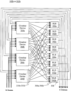
Figure 7 illustrates one implementation of nested function blocks 602a-
b. Nested function blocks 602a-b include 4 programmable function blocks
702a-d (for the purpose of illustration, blocks 702a-d are represented two
times
to clarify the input and output connection pattern), 4 crossbar devices 704a-
d,
12 inputs, 12 outputs and connections 750 752 754 756. Crossbar devices
704a-d are the first, second and third subsets of crossbar devices at the
nested
function block level, respectively routing the inputs to the function block
702a-d
inputs through connections 756 750, the function block 702a-d outputs to the
function block 702a-d inputs through connections 754 750 and the function
block 702a-d outputs to the outputs through connections 754 752. Accordingly,
nested function block 702a-d topologically occupy the positions of function
blocks 202 of the nested function block level, crossbar devices 704a-d
topologically occupy the positions of crossbar devices 204 of the nested
CA 02461540 2004-03-23
WO 03/032492 PCT/EP02/11075
function block level, and connections 750 752 754 756 topologically occupy
respectively the positions of connections 250 252 254 256 of the nested
function block level. Programmable function blocks 702a-d are the same
implementation of the programmable function block described above and
illustrated in Figure 3.
Note that each of the crossbar devices of IC 500 has a fixed number of
inputs and a fixed number of outputs, and therefore one important
characteristic of the present invention is that signal is always propagating
through the crossbar devices in the same direction. But the present invention
may be practiced with any kind of crossbar device architecture like pass
transistor bi-directional crossbar device or wired-or unidirectional crossbar
device or buffered uni-directional crossbar device.
Further, all connections between the crossbar devices of IC 500 are
done accordingly with the rules disclosed above and illustrated Figure 4.
Note that for ease of illustration and understanding, IC 500 is purposely
illustrated with a small number of elements. However, those skilled in the art
will appreciate that IC 500 implementation may be scaled up to realistically
represent a commercial product. For example:
a) IC level may include 16 "48-inputs 48-outputs" crossbar devices, 1
first level nested function block, 384 input pins and 384 output pins;
b) first level nested function block may include 48 "32-inputs 48-
outputs" crossbar devices, 24 second level nested function block,
384 inputs and 384 outputs;
c) second level nested block may include 16 13-inputs 35-outputs
crossbar devices, 8 programmable function blocks, 80 inputs and 48
outputs; and
d) programmable function block may include 4 "20-inputs 16-outputs"
crossbar devices, 16 "4-inputs 1-output" RLEs, 64 inputs and 16
outputs.
Accordingly, IC has 3092 RLEs, 384 external output pins and 384
external input pins.
Thus, a fully or partially reconfigurable integrated circuit having a
scalable architecture has been described. While the integrated circuit of the
to
CA 02461540 2004-03-23
WO 03/032492 PCT/EP02/11075
present invention has been described in terms of the above illustrated
embodiments, those skilled in the art will recognize that the invention is not
limited to the embodiments described. Further, while the present invention has
been described as an integrated circuit, the present invention may be
practiced
as an embeddable logic block forming a portion of an IC instead. Accordingly,
the present invention can be practiced with modification and alteration within
the spirit and scope of the appended claims. The description is thus to be
regarded as illustrative instead of restrictive on the present invention.
n