Note: Descriptions are shown in the official language in which they were submitted.
CA 02461541 2004-03-23
WO 03/032532 PCT/GB02/04125
OPTICAL SIGNAL TRANSMISSION
This invention relates to optical signal transmission and more especially to
an apparatus for,
and a method of, transmitting a plurality of data signals (communication
channels). In
particular the invention concerns optical signal transmission for use in dense
wavelength
division multiplex (DWDM) optical telecommunication networks.
As is known in DWDM optical telecommunication networks a plurality (typically
40, 80,
160 or higher) of communication channels are transmitted by modulating a
respective
optical carrier having a discrete waveband, and then transmitting the
plurality of modulated
optical carriers (WDM radiation) along a single optical fibre. Typically each
modulated
optical carrier is generated by amplitude (intensity) modulating a continuous
wave (cw)
optical carrier generated by a respective laser using a respective optical
modulator (e.g. a
Mach- Zehnder optical modulator). It is also lcnown to include a further
respective optical
modulators for modulating (e.g. phase modulation or pulse shaping) each of the
modulated
carriers before combining (multiplexing) them to form the WDM radiation for
transmission. The control of such transmission apparatus is complex due to the
large
number of optical modulators involved especially for networks involving 80 or
more
channels. Additionally they are expensive due to the large number of
modulators.
The present invention has arisen in an endeavour to provide an improved
optical
transmission apparatus that, at least in part, overcomes the limitations of
the known
arrangements.
CA 02461541 2004-03-23
WO 03/032532 PCT/GB02/04125
2
According to the present invention there is provided an optical signal
transmission
apparatus for transmitting a plurality of data signals comprising: a plurality
of input means
for receiving a respective one of the data signals and delivering the
respective data signal
with a controlled phase and at a controlled data rate; optical carrier
generation means for
generating a plurality of optical carrier signals having different
wavelengths; a plurality of
first modulation means each being for modulating a respective one of the
optical carriers
with a respective data signal to provide a first-modulated optical carrier
signal; and an
optical signal-routing device having a plurality of input ports, each port
being for receiving
a respective one of the first-modulated optical carrier signals and delivering
it to the output
to port of the device, characterised by: further modulation means for further
modulating each
of the first-modulated optical carrier signals in dependence upon a clock to
provide a
plurality of further-modulated optical carrier signals; and a feedback
arrangement,
including the optical signal-routing device, for feeding back a proportion of
each of the
further-modulated optical carrier signals to a respective input means for
controlling the
is phase and rates at which the input means delivers the data signal to the
first modulation
means in dependence upon the further modulation to thereby synchronise each
input data
signal to the clock and wherein the optical signal-routing device delivers
each of the
further-modulated signals applied to its output to a respective input means
along a path
which is dependent upon the wavelength of the signal.
The present invention provides the advantage that each to of the data signals
can be
synchronised with a minimum of additional components; °namely a single
further optical
modulator and the optical signal-routing device to provide a respective
feedback path to
CA 02461541 2004-03-23
WO 03/032532 PCT/GB02/04125
3
each input means. Synchronisation of each data signal is advantageous in that
it enables
modulation to occur in the centre bit window for each data signal thereby
enabling a single
further modulator to be used to pulse shape all of the modulated carriers. In
contrast in the
known transmission apparatus a further respective modulator is used to pulse
shape a
respective one of the plurality of modulated optical Garners.
Preferably, the apparatus further comprises: a plurality of first optical
directional couplers
so connected as to convey the plurality of first-modulated optical carrier
signals to the input
ports of the optical signal-routing device and to convey the signals conveyed
by the
to feedback arrangement from the input ports of the optical signal-routing
device towards the
plurality of input means and a second optical directional coupler so connected
as to convey
the plurality of first-modulated carrier signals from the output port of the
optical signal-
routing device and to convey the signals conveyed by the feedback arrangement
to the
output port of the optical signal-routing device.
Conveniently the optical directional couplers are polarisation dependent
couplers that
operate as beam-splitting devices in one direction and beam-combining devices
in the
opposite direction. With such couplers the apparatus advantageously further
comprises:
means, in a feedback path between the further modulation means and the second
optical
directional coupler, for providing a 90° rotation in the polarisation
of signals conveyed by
the path. Preferably such a feedback path comprises a polarisation maintaining
optical fibre
into which a 90° twist has been introduced.
CA 02461541 2004-03-23
WO 03/032532 PCT/GB02/04125
4
Alternatively the first and second optical directional couplers can be optical
circulators, in
which case the feedback path need not provide a 90° rotation in the
polarisation of signals
conveyed by the feedback path.
Preferably, the optical signal-routing device comprises an arrayed waveguide
router.
In one arrangement, the further modulation means comprises a pulse-shaping
modulator.
In an alternative arrangement, the further modulation means comprises a phase
modulator.
In a further alternative arrangement, the further modulation means comprises a
pulse-
shaping modulator connected in series with a phase modulator.
Preferably, the input means includes a buffer store capable of storing input
signal data and
delivering the signal data at the controlled rate.
The invention also provides a method of transmitting a plurality of data
signals comprising:
delivering the plurality of data signals with controlled phase at controlled
rates; modulating
a plurality of different-wavelength optical carrier signals with the data
signals; conveying
2o the plurality of different-wavelength modulated optical carrier signals to
respective input
ports of an optical signal-routing device, passing the plurality of different-
wavelength
modulated optical carrier signals through the optical signal-routing device
which delivers
the modulated optical carrier signals to its output port along respective
paths through the
CA 02461541 2004-03-23
WO 03/032532 PCT/GB02/04125
optical signal-routing device dependent on the wavelengths of the optical
carrier signals;
subjecting the different-wavelength modulated optical carrier signals to
further modulation
at a set rate; transmitting the different-wavelength modulated optical carrier
signals
following the further modulation; and controlling the phase and rate of
delivery of the
5 plurality data signals in accordance with the phase and rate of further
modulation.
An optical signal transmission apparatus in accordance with the invention will
now be
described by way of example only with reference to the accompanying drawing
which is a
diagrammatic representation of a WDM (Wavelength Division Multiplexing)
optical signal
1o transmission apparatus for transmitting a plurality of electrical data
signals to produce a
corresponding WDM optical output radiation.
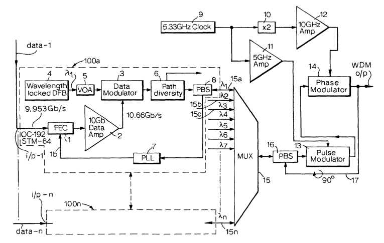
Referring to the accompanying drawing, the WDM optical signal transmission
apparatus
comprises a plurality n of data input ports i/p-1 to i/p-n for receiving a
respective electrical
data input signal data-1 to data-n. Each data input port i/p-1 to i/p-n is
associated with a
respective first-modulation circuit block 100a to 100n.
The components and interconnections of the first-modulation circuit block 100a
associated
with the input signal data-1 will now be described.
zo
The data input port i/p-1 is provided by a signal input port of a forward
error correction
(FEC) circuit 1 which has a control input port 1b through which the FEC
circuit 1 is
synchronised to an external control signal/clock. The output port of the FEC
circuit 1 is
CA 02461541 2004-03-23
WO 03/032532 PCT/GB02/04125
6
connected to the signal input port of an amplifier 2. The output port of the
amplifier 2 is
connected to a modulating-signal input port of an optical modulator 3 (e.g.
Mach-Zehnder
optical modulator) which includes an optical carrier-signal input port
connected to a
wavelength-locked distributed feedback laser (DFB) 4 through a variable
optical attenuator
(VOA) 5. The output port of the optical modulator 3 is connected to a signal
input port of a
path diversity control circuit 6 and the output port of the path diversity
control circuit 6 is
connected to a first port of a first polarisation beam splitter/combiner (PBS)
8. The PBS 8
includes a first output port which constitutes an optical output of the first-
modulation
circuit block 100a and a second output port which is connected through a phase
locked loop
to (PLL) element 7 to the control input port 1b of the FEC 1.
The optical output of each first-modulation circuit block is connected to a
respective input
port 15a to 15n of an optical multiplexes 15. The output port of the optical
multiplexes 15
is connected to a first port of a second polarisation beam splitter/combiner
(PBS) 16, a
second port of which is connected to a signal input port of an optical pulse-
shaping
modulator 13. The optical signal output port of the pulse-shaping modulator 13
is
connected to a signal input port of an optical phase modulator 14, the output
port of which
serves as the output port of the transmission apparatus. The output port of a
control clock
oscillator 9 is connected through an amplifier 11 to an electrical control
port of the pulse-
2o shaping modulator 13. The output port of the control clock oscillator 9 is
connected also to
the control port of the phase modulator 14 through a frequency-doubling
circuit 10 and an
amplifier 12. An optical feedback path 17 extends from the output port of the
phase
modulator 14 to a third port of the second PBS 16. The optical feedback path
17 introduces
CA 02461541 2004-03-23
WO 03/032532 PCT/GB02/04125
7
a 90° rotation in the plane of polarisation of an optical signal
passing through the path.
Preferably the feedback path 17 comprises a polarisation maintaining optical
fibre into
which a 90° twist has been introduced.
As described the optical multiplexer 15 has a plurality of signal input ports
15a, 15b,
15c...15n each associated with a respective first-modulator circuit block
100a, 100b ...
100n. The multiplexer 15 passively combines (multiplexes) the plurality of
optical input
signals of different wavelengths applied to the signal input ports 15a, 15b,
15c...15n and
delivers the combined WDM signal to its single output port. Conversely, an
optical signal
applied to the single output port of the multiplexer 15 follows a path
determined by the
wavelength of the optical signal and reaches an input port corresponding to
the wavelength
of the optical signal. The optical multiplexer 15 thus operates as a de-
multiplexer in this
reverse direction.
As described, the FEC circuit 1, PLL circuit 7, amplifier 2, optical modulator
3,
wavelength-locked DFB laser 4, VOA 5, path diversity control circuit 6 and PBS
8 form a
first-modulation circuit block 100a as shown within the dotted lines and
additional first-
modulation circuit blocks represented by the dotted enclosure 100n are
connected to the
other signal input ports 15b, 15c...15n of the optical multiplexer 15. The
first-modulation
2o circuit blocks 100a....100n are independent of one another and can be added
as needed.
The first-modulation circuit blocks are, advantageously, fabricated as circuit
boards having
an electrical input port and an optical output port capable of connection to a
respective
optical input port of the multiplexer 15. Additional first=modulation circuit
blocks 100n
CA 02461541 2004-03-23
WO 03/032532 PCT/GB02/04125
8
need not occupy consecutive positions in relation to the input ports 15b...15n
of the
multiplexer 15.
The optical multiplexerlde-multiplexer 15 is preferably an arrayed waveguide
(AWG)
router which is passive and includes a substantial number, a few hundred, say,
of input
ports. The AWG router has the intrinsic characteristic that the path taken by
light passing
through it depends on the wavelength of the light and, as a result the inputs
of such a device
are wavelength specific. Importantly for the present invention an optical
signal applied to
the output port of the multiplexer 15 travels to an input port determined by
the wavelength
to of the optical signal. The AWG router may be of glass fabrication.
The FEC circuit 1 includes a plurality of buffer circuits capable of storing
(buffering) the
input data elements. The stored data elements are delivered to the output port
of the FEC
circuit 1 under the control of a clock signal applied to the control input
port 1b of the FEC
circuit 1. The FEC circuit 1 enables incoming data streams data-1 to data-n
with phase and
frequency drifts around a standard rate, for example, STM-64 or OC-192 data
rate, to be
converted to a common clock rate. Although the FEC circuit 1 performs both the
function
of forward error correction and the function of rate conversion, these
functions can be
separated, forward error correction being performed in a circuit which does
not adjust the
2o data rate and rate conversion being performed in a circuit without error-
correction
capability. The order in which the two functions are performed is immaterial
if separate
circuits are used.
CA 02461541 2004-03-23
WO 03/032532 PCT/GB02/04125
9
The apparatus is operable with a fixed power output level from the DFB laser 4
and it thus
follows that the VOA 5 is not essential to the apparatus.
The apparatus can include a pulse-shaping modulator alone or a phase modulator
alone.
Alternatively, an amplitude/phase modulator may be used in place of both the
pulse-
shaping modulator 13 and the phase modulator 14.
The path diversity circuit 6 is not essential to the apparatus in that it
performs a safety
function by effecting switching from a main fibre path to another fibre path
in the event of
to a fault condition occurring on the main fibre path. The PBS 8 functions to
pass input
signals at its first port to its second port acting as an output port and,
also, to pass input
signals at its second port, acting as an input port, to its third port acting
as an output port.
The PBS 16 functions in a similar manner to the PBS 8 in passing signals from
its first to
its second port and, also, from its second port acting as an input port to its
third port. The
i5 PBS 8, 16 route optical signals in dependence upon there polarisation
state.
The 90° rotation in the plane of polarisation of the optical energy in
the reverse direction
relative to the forward direction, through the PBS 8 and the PBS 16, is
required in order to
permit the PBS 8 and the PBS 16 to separate the reverse energy from the
forward energy.
The PBS 8 and the PBS 16 can be replaced by optical signal circulators in
which case the
optical feedback path 17 does not need to provide a 90° rotation in the
polarisation of the
feedback signal from the output of the apparatus.
CA 02461541 2004-03-23
WO 03/032532 PCT/GB02/04125
The operation of the optical transmission apparatus will now be described with
reference to
a data signal applied to the input port i/p-1. The electrical data signal data-
1 arrives at
9.953 Gb/s at the signal input port i/p-1 and receives additional bits for
forward error
5 correction in the FEC circuit 1, bringing the data rate to 10.66 Gb/s, under
the timing of the
control clock oscillator 9 through the feedback connection to the control
input port 1b of
the FEC circuit 1. This electrical data signal is amplified by the amplifier 2
and the
amplified signal is used to control the optical modulator 3. An optical
carrier signal, of a
selected wavelength ~1, is generated by the wavelength-locked DFB laser 4 and
the level of
1o the optical carrier signal is adjusted by the VOA 5 before it enters the
optical modulator 3
where the optical signal is amplitude-modulated by the 10.66 Gb/s data signal.
The
modulated optical carrier from the modulator 3 passes to the path diversity
control circuit 6
from which it goes to its respective input port 15a of the multiplexes 15
through the PBS 8.
The modulated optical carrier travels to the single output port of the
multiplexes 15 along
an optical path determined by its wavelength as is indicated above.
The optical signal output from the output port of the multiplexes 15 passes
through the PBS
16 and the form of the signal is subjected to pulse-shaping in the pulse-
shaping modulator
13. The signal leaving the pulse-shaping modulator 13 is next subjected to
some form of
2o phase-modulation, for example, modulation effecting frequency chirp to pre-
compensate
for chromatic dispersion during subsequent transmission of the WDM radiation
over the
transmission fibre, in the phase modulator 14. The pulse-shaping modulator 13
is
synchronised to the clock oscillator 9 through the connection of the control
clock oscillator
CA 02461541 2004-03-23
WO 03/032532 PCT/GB02/04125
11
9, by way of the amplifier 11, to the control port of the pulse-shaping
modulator 13. The
phase of the signal is adjusted to the phase of the control clock oscillator 9
through the
connection of the control clock oscillator 9 to the control port of the phase
modulator 14 by
way of the frequency doubling circuit 10 and the amplifier 12.
The clock signal for the FEC 1 is recovered from the output signal from the
phase
modulator 14 by way of a feedback circuit comprising the optical feedback path
17, the
PBS 16, the multiplexer 15, the PBS 8 and the PI L 7. Through this clock
signal the phase
and rate of the FEC 1 is adjusted to synchronise each of the first-modulator
circuit blocks to
1o the control clock oscillator 9 and thereby ensure modulation occurs in the
centre bit
window for each electrical data input signal.
The feedback circuit is an.essentially an all optical feedback circuit. The
feedback element
17, the PBS 16, the optical multiplexer 15 and the PBS 8 are all optical
elements and the
feedback circuit is compact in that it requires only the optical feedback
element 17 and the
PLL 7 as additional components. The PLL 7 of course includes some form of
optical to
electrical conversion for converting the fed back optical signal to an
electrical signal from
which the clock signal can be derived.
2o The characteristic of the multiplexer/de-multiplexer 15 in separating
signals of different
wavelengths travelling from its single output port to its input ports
15a...15n avoids the
need for separate signal connections (feedback paths) between the PBS 16 and
the
respective polarisation beam splitters/combiners such as the PBS 8.
CA 02461541 2004-03-23
WO 03/032532 PCT/GB02/04125
12
The frequency of 5.33 GHz used for the control clock oscillator 9 represents
one possible
clock frequency for the apparatus. Other clock frequencies may be used and, in
general, the
clock frequency is so chosen that the pulse-shaping modulator 13 and the phase
modulator
14 operate at the line rate which is dictated by the specific arrangement of
the system to
which the apparatus belongs.
The output optical fibre of the phase modulator 14 includes a tap from which a
proportion
of the W1~M output signal is fed back through the feedback path 17. The
90° rotation of the
1o polarisation introduced by the feedback path permits the use of the PBS 16
and the PBS 8
to distinguish between the forward propagating and fed back signals. The use
of
polarisation beam splitter (PBS) that route optical signals in dependence upon
their
polarisation state enables low-loss coupling of the return signal.
The use of the multiplexer 15 as both a multiplexer and a de-multiplexer
accommodates the
forward and return signals with a minimum of additional components. As is
indicated
above, the PBS 8 and the PBS 16 may be replaced by optical signal circulators
in which
case there is no need for the optical feedback path 17 to introduce a
90° rotation of
polarisation.
Similarly to the above situation for the signal present at the first signal
input port 15a of the
multiplexer 15, respective further signals present at the second, third
....na' signal input
ports 15b, 15c...15n of the multiplexer 15 travel through the multiplexer 15
between the
CA 02461541 2004-03-23
WO 03/032532 PCT/GB02/04125
13
input ports and the single output port, both forwards and backwards, along
paths
determined by their wavelengths.
The feedback path 17 preferably uses an existing fibre patch/back-plane and,
consequently,
requires no new board-to-board connections.
As is indicated above, the elements 1, 2, 3, 4, 5, 6, 7 and ~ may be provided
in a unit
containing the first-modulation circuit block for a particular channel and
need only be
provided when the particular channel in included in the apparatus. These
elements may be
to assembled as a first unit while the remainder of the apparatus is assembled
as a second unit.
The second unit includes the multiplexer 15, the PBS 16, the pulse-shaping
modulator 13,
the phase modulator 14, the feedback element 17 and the clocking components 9,
10, 11
and 12, the first and second units being joined to each other by a plurality
of optical links
corresponding to the input ports of the multiplexer 15.
The optical signal transmission apparatus is especially suitable for
transmission including
return-to-zero (R-Z) data generation in high-speed dense wavelength division
multiplexed
(DWDM) networks although, in the present example, the input electrical data
signal present
at the input port i/p-1 is a non-return-to-zero (NRZ) data signal. The
alignment of the
2o phases of the modulator 3 drive signals is effected in order to ensure that
modulation occurs
in the centre of the bit window for each channel. In the apparatus, the pulse-
shaping
modulator 13, which is shared by all of the channels, is driven by the fixed
control clock
oscillator 9 and the data channels are aligned with the pulse-shaping
modulator 13 through
CA 02461541 2004-03-23
WO 03/032532 PCT/GB02/04125
14
the optical feedback path to the FEC 1.
In an optical signal transmission apparatus capable of 160-wavelength channel
operation
(i.e. n = 160), an optical modulator 3 is required for each channel. As
regards the pulse-
s shaping modulator 13 and the phase modulator 14, an advantageous
arrangement, based on
the above apparatus, employs one of each of those modulators for 40 channels,
that is, the
multiplexer 15 has 40 input ports, resulting in a need for four pulse-shaping
modulators and
four phase modulators for the full 160 channels.
1o Known optical signal transmission apparatus capable of equivalent operation
to the
transmission apparatus of the present invention require a modulator, a pulse-
shaping
modulator and a phase modulator for each channel, that is, the conventional
requirement is
for 160 data modulators, 160 pulse-shaping modulators and 160 phase modulators
for 160
channel operation. The modulated optical carriers, representing a respective
WDM
15 channel, are then multiplexed together to provide the WI~M output.
The optical signal transmission apparatus of the present invention is
particularly suited to a
transmitter in an optical fibre transmission system and a plurality of the
transmitters
together with interface devices serve the function of a transponder capable of
transmitting
several times the plurality of data signals.