Note: Descriptions are shown in the official language in which they were submitted.
CA 02461862 2004-03-25
System and Method for Detecting Connector Pin Insertion in Printed Circuit
Board
Assemblies
This invention relates to a system and method for detecting connector pin
insertion in printed circuit board assemblies.
BAGKGROUND OF THE INVENTION
As printed circuit board assemblies (PCBA) are increasing in size, complexity,
and
speed of operation, the mating of such PCBAs to one-another requires the use
of
high-density connector assemblies. For example, in a complex router electronic
circuit application, the line-card PCBA must typically be mated to a mid-plane
PCBA
to perform the routing tasks once the product is deployed.
To permit such mating, the industry uses press-fit connectors that may include
hundreds of pins. These connector assemblies are pressed in place on a grid of
pre-drilled wells of a PCB.
The connector manufacturing process inaccuracies and the press fitting process
may cause some of the pins to collapse, thus creating a defective PCBA. These
defects may harm the PCBA, either when power is initially applied to the
finished
product, or over time, when temperature cycling may cause some of the
misaligned
pins to dislodge or lose contact with the wall of the wells.
PCBAs are typically subject to manual visual inspections during manufacturing
in
order to intercept defective ones. In some cases, automatic optical inspection
or
laser based measurement by triangulation are carried out.
The complexity and density of high-density connector assemblies has rendered
the
task of inspecting for proper assembly nearly impossible, either automatically
or by
manual inspection means. Thus, it is not currently possible to determine
whether a
pin is inserted, or whether it is inserted to the appropriate height.
CA 02461862 2004-03-25
2
It is therefore preferable to provide a system that allows inspection of PCBAs
that
embed such high-density connectors as part of the finished PCBA.
SUMMARY OF THE INVENTION
It is an object of the invention to provide a novel system and method for
detecting correct pin insertion in PCB assemblies that obviates or mitigates
at least
one of the disadvantages of existing systems.
The present invention uses a laser-based sensor to detect pin locations in
wells of PCBs.
In accordance with an aspect of the invention, there is provided a pin
detection system for detecting connection pin insertion in a printed circuit
board
assembly. The system comprises a conveyer , a stage assembly, and a sensor.
The conveyer is provided for conveying the printed circuit board assembly
under
test at the appropriate resting place where it will be inspected. The stage
assembly
is used to convey the sensor to specific areas of interest of the PCBA under
test for
the purposes of measuring pin height information. The printed circuit board
assembly comprises a printed circuit board having multiple wells and one or
more
connectors having pins that are inserted into the wells of the printed circuit
board.
The sensor is provided for detecting pin insertion in the wells using a laser
beam.
In accordance with an aspect of the invention, there is provided a
method of detecting connection pin insertion in a printed circuit board
assembly.
The method comprises the steps of conveying a printed circuit board assembly
under test, the printed circuit board assembly comprising a printed circuit
board
having multiple wells and one or more connectors having pins that are inserted
into
the wells of the printed circuit board; and detecting pin insertion in the
wells using a
laser beam.
Other aspects and features of the present invention will be readily apparent
to
those skilled in the art from a review of the following detailed description
of preferred
embodiments in conjunction with the accompanying drawings.
BRIEF DESCRIPTION OF THE DRAWINGS
CA 02461862 2004-03-25
3
The invention will be further understood from the following description with
reference to the drawings in which:
Figure 1 is a block diagram showing a pin detection system in accordance
with an embodiment of the present invention;
Figure 2 is a block diagram showing a pin detection system suite in
accordance with another embodiment of the present invention;
Figure 3 is a schematic view showing an example of connector;
Figure 4 is a schematic view showing an example of a well of a PCB;
Figure 5 is a schematic view showing an example of a pin fit in the well;
Figure 6 is a schematic views showing the operation of the pin detection
system;
Figure 7 is a graph showing an example of measurements;
Figure 8 is a schematic plan view showing an example of a panel under test;
Figure 9 is a schematic bottom view of the panel under test;
Figure 10 is a schematic view showing an example of a laser beam of the pin
detection system;
Figure 11 is a diagram showing an example of a database data structure;
Figure 12 is a graph showing an example of measurement results;
Figure 13 is a graph showing a detailed view of measurement results;
Figure 14 is a graph showing the detailed view indicating areas of interest;
and
Figure 15 is a photograph showing an example of a pin tip inserted in a well.
DETAILED DESCRIPTION OF THE PREFERRED EMBODIMENTS
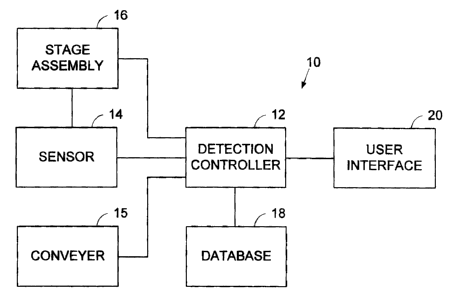
Figure 1 shows a pin detection system 10 in accordance with an embodiment
of the invention. The pin detection system 10 comprises a detection controller
12,
sensor 14, conveyer 15, stage assembly 16, database 18 and user interface 20.
The pin detection system 10 is suitably used for inspection of printed circuit
board assemblies (PCBAs) that embed on PCBs one or more connectors as part of
the assemblies. PCBs have through holes coated with conductive materials (also
referred to as "wells" hereinafter). Connectors have pins which are inserted
into the
CA 02461862 2004-03-25
4
through holes of PCBs. The pin detection system 10 allows inspection of pin
connections during the manufacturing cycle of the PCBAs and prior to applying
electric power to the PCBAs. Thus, defective PCBAs can be intercepted.
As shown in Figure 2, the pin detection system 10 may be used as part of a
defect detection system suite 25.
The detect detection system suite 25 checks for correct seating of high-
density press fit connector pins in PCBAs. The pin detection system 10
performs
inspection of PCBAs using templates generated with information available in
PCB
design files and component data sheets.
The defect detection system suite 25 comprises the pin detection system 10,
a design centre 32 and repair centre 34 which are interconnected by a
corporate
network 30.
The design centre 32 is used by a designer to program the configuration of
the PCB assemblies that will be inspected with the pin detection system 10.
The
design centre 32 is used to describe pins, wafers, connectors, and how those
connectors are arranged on a PCB assembly panel. The design centre 32 has
many features to facilitate the programming task, including the extensive use
of
templates.
The pin detection system 10 performs PCB assembly inspections in
accordance with the programs) that have been defined with the design centre
32.
The pin detection system 10 can be used by three types of operators to ensure
smooth integration of the unit in the plant operations:
o The Programmer - Once the design information has been codified with the
design centre 32, the pin detection system 10 is trained by the programmer to
locate
the panel in space and then scan the various connectors for the purposes of
measuring pin height information;
o The Machine Operator - Once the pin detection system 10 has been trained
to inspect a particular product, the machine operator uses the pin detection
system
10 to inspect panels at the appropriate point in the manufacturing process;
o The Maintenance Operator - Specific on-board capabilities are used by the
machine operator to rapidly assess machine readiness and fitness for use.
CA 02461862 2004-03-25
c
The repair centre 34 permits the viewing of fault information written to the
product database after the panels have been inspected by the pin detection
system
10. After a panel has been repaired, the operator can reclassify faults to
reflect the
disposition of the fault or the panel.
5 In the embodiment shown in Figure 2, the design centre 32 and repair centre
34 are provided separately from the pin detection system 10. In a different
embodiment, the design centre 32 and/or repair centre 34 may be integrated in
the
pin detection system 10.
The embodiments of the invention are further described hereinafter in
connection with inspection of a PCBA having press fit connectors.
The invention may be used for PCBAs having different type of connectors
whose pins are inserted into through hole of PCBs. Connectors are press fit
using a
press, such as a computer-controlled servo-electric presses. By inspecting all
press
fit pins, the pin detection system 10 allows further processing of only those
PCBAs
that have the press-fit pins seated correctly and are at the right depths.
An example of a press fit connector 100 is shown in Figure 3. The connector
100 comprises one or more wafers 104 having multiple pins 106. Each pin 106
has
a diameter of 0.5 mm and depth of 3.175 mm in this example. In a different
model
of wafers, smaller or larger pins may be provided. The pin detection system 10
may
be suitably used to inspect connectors having pins that are suitable for
insertion into
wells of about 0.35 to 0.75 mm diameters. Pins 106 are provided at 1.5 mm
interval. The wells are plated with conductive materials. Multiple wafers 104
are
aligned together so that pins 106 in neighbouring wafers 104 are spaced apart
at
1.8 mm. Rather than combining multiple wafers, a single wafer may have a
plurality
of rows of pins. Pins 106 are inserted in the holes in one pressing operation.
Connectors may have multiple pins 106, such as 1800 pins 106 pressed in one
occurrence. Connects having different geometry may be used for different
PCBAs.
Figure 4 shows a schematic partial view of a PCB 110 on which the connector
100 is connected using press fit pins 120 (Figure 5). The PCB 110 has through
holes or wells 112 coated with conductive material 114. This PCB 110 has a
thickness of 3.175 mm. The diameter of the well 112 is 0.5 mm. Different PCBs
may be used for different connectors and pins and wafer types. The geometries
of
CA 02461862 2004-03-25
k
6
PCBs and connectors are codified with the design center 32 as templates, once
only
for each pin/wafer/connector model, as further described below .
Figure 5 shows an ideal insertion of a press fit pin 120 in the well 112 of
PCB
110 when the connector 104 is mounted onto the PCB 110 from the bottom in this
drawing. The press fit pin 120 has an insertion tip 122 and an enlarged
section 124
with a hole 126. The enlarged section 124 has a diameter larger than the
diameter
of well 112 prior to the insertion into the well 112. When the press fit pin
120 is
inserted into the well 112, the enlarged section 124 deforms to fit into the
well 112.
Different types of press fit pins may be used in different embodiments.
Ideally the press fit pin 120 is inserted into the well 112 so that a
predetermined distance is left between the insertion tip 122 of the press fit
pin 120
and an opening end 113 of the well 112. In this example, the predetermined
distance is 1.016 mm.
Referring back to Figure 1, the sensor 14 of the pin detection system 10
measures the distance between the insertion tip 122 of each press fit pin 120
and
the opening end 113 of its respective well 112, i.e., the insertion depth of
the press
fit pin 120 in the well 112.
The sensor 14 measures the insertion depth of press fit pins 120 in wells 112,
utilizing laser-based interferometer to measure distances. The sensor 14 emits
a
laser beam and detects reflected laser beam.
Laser-based interferometer permits a laser beam that is tight enough to
enable focusing the beam on the tip of a pin that is recessed under the panel,
without excessive artifacts due to beam that intersects at the opening end 113
of the
well.
Figure 10 shows an example of beam geometry that is suitably used for
measuring a PCBA that embeds a connector having a press fit pin 120 with an
insertion tip 122 of 0.0133 mm and 0.052 mm. The beam 150 has an ideal focus
point of 38.0 mm. It has 1.5 degrees, 1 mm and 6 degrees, 4 mm at the emission
end, and 0.375 mm and 0.15 mm at 1.5 mm from the ideal focus point.
The sensor 14 may be a holography measurement system in which an
interference fringe pattern is encoded in the incident beam. By using such an
interterence fringe pattern, it is possible to eliminate the need for a
mechanical
CA 02461862 2004-03-25
K
7
system having moving part, which is costly, unreliable and slow, to adjust the
so-
called "reference" arm used in the interferometry technique. This type of
sensor 14
permits high speed measurements, such as 20 measurements inside a typical well
112, while traveling rather fast on the surface.
Figure 6 shows an example of an operation of the sensor 14. The sensor 14
is operated to scan a well 112 from one edge to the diametrically opposite
edge so
that a laser beam 130 scans through the insertion tip 122 of the press fit pin
120 in
the well 112. Figure 7 shows an example of the detected reflection of the
laser
beam 130. Initially, the laser beam is reflected by the surface of the PCB
110,
which is measured as approximately 1.5 mm in this example. The reflection
drops
when the laser beam 130 comes to an edge of the well 112 and then reach to a
peak when the laser beam 130 reaches to the insertion tip 122 of the pin 120,
which
is typically measured as approximately 0.1 to 0.8 mm depending on the
insertion of
the pin 120. If the pin is missing, there will be no peak in the measurements.
The sensor 14 may obtain two types of measurement characteristics. For
each data point, the sensor 14 may measure the distance to a focal point (D),
as
well as Signal to Noise Ratio (SNR). Whilst the D measurement could be enough
for certain purposes, it is preferable to use SNR to refine the spatial
registration of
the point since the SNR measurement allows auto-correlation with the
theoretical
position of the wells. This supports the algorithms for spatial alignment and
pin-
computation, which are described below.
The pin detection system 10 carries out two types of measurements: point
based measurements and trace based measurements.
The point based measurements are carried out when the pin detection
system 10 uses the stage 16 to move the sensor 14 to a known location. The pin
detection system 10 measures the (DISNR) combo at that point. The measured
(D/SNR) value is typically used in the following contexts:
o When determining the reference height of the surface of the panel under
test, near a region of interest (for example near a connector);
, o When adjusting the standoff of the laser so as to place the beam's focal
point at the ideal position;
CA 02461862 2004-03-25
c
o When re-measuring a specific pin's height, when the other processes have
failed;
o When re-asserting a "missing pin" defect classification, to provide multiple
data points as objective evidence to the classification; and
o When attempting to locate a hole's x-y coordinates.
The trace based measurements are carried out when the pin detection
system 10 places the laser beam at a start point (Ps) and while traveling to
an end
point (Pe). The pin detection system 10 measures and captures a point every ~X
or
~Y units of distance. For example, when going from Ps=(1.0,2) to Pe =
(2.0,2.0),
the pin detection system 10 captures a point every 0.001 inches, thus
performing
1001 measurements. The data are stored on a data storage, such as a disk, for
later analysis of the trace content. The trace content obtained for the above
example has
1, 1.000, 2.000, hh.h(1 ), nn.n(1 )
2, 1.001, 2,000, hh.h(2),nn.n(2)
through
1001, 2.000, 2.000, hh.h(1001), nn.n(1001)
where hh.h is the distance from focal point in mils and nn.n is the signal-to-
noise
ratio for the data point.
The trace based measurements are used in a number of situations, such as:
o When measuring an entire row of pins, for later bulk-computation;
o When determining the location (x,y) of a hole in space;
o When remeasuring a specific pin's height; and
o When re-asserting a "missing pin" defect classification, to provide multiple
data points as objective evidence to the classification.
In point-based measurements, the data is processed immediately to permit
an instantaneous decision on the part of the adaptive algorithms, and thus
permit a
rapid inspection process.
In trace-based measurements, the data may be stored on disk or other data
storage in a sequential file, for later analysis and processing.
CA 02461862 2004-03-25
9
Referring back to Figure 1, the conveyer 15 ingress/egress PCBAs under test
into or out of the pin detection system 10. When a PCBA is mounted on the
conveyer 15, it ingresses the PCBA underneath of the sensor 14.
The stage assembly 16 controls the positioning of the sensor relative to the
PCBA ingressed by the conveyer 15 so that the laser beam is brought to the
area of
interest on the PCBA.
The pin detection system 10 may use a adaptive motion system. The
adaptive motion system permits to compensate for operational variations, and
to
perform inspections based on design data (invariant). The adaptive motion
system
has the following major functions:
~ The adaptive motion system implements the theoretical-to-actual
transformation of coordinates in real time, discharging the defection system
10 from the responsibility of performing that task. Thus the Motion System
adapts to variations in panel placement.
~ The adaptive motion system uses low cost part for the mechanical
implementation of the motion system. These parts can have significant non-
linearity or distortions. The adaptive motion system is programmed to
compensate for these non-linearity and distortions, thus providing the
benefits of very high positional accuracies (e.g., fewer than 0.1 mil in any
axis).
~ Heavy parts on the PCB can cause the PCB under test to droop, causing
significant variations of the reference plane height (PCB surface) over the
inspection area. The adaptive motion system compensates for pre-measured
droopiness and thus permits the recording of pre-flattened traces, at the
appropriate reference plane height. This facilitates the computational burden
of trace-based measurement analysis. Also, this extends the depth-of-field of
the focused laser beam, since the focal point is always at the exact optimal
distance from the PCB surface. Deeper pins can be measured.
The preferred embodiment uses the adaptive motion system to compensate
for motion related operational variations. Alternative embodiments may use
more
expensive motion system components (such as high precision screws, linear
CA 02461862 2004-03-25
motors) to improve positional accuracy, or may use a levelling piston to
straighten
the PCB under test, thus eliminating the need to adapt to surface curvature.
As shown in Figure 8, when a PCBA or panel under test 140 is mounted on
the conveyer 15, the detection controller 12 performs a panel registration
process to
5 register the panel 140. The panel registration process may be carried out
using a
reference hole 142 on the panel 140, such as a tooling hole, that is
sufficiently large
to facilitate machine training. Also the panel registration process uses two
fiducial
holes 144 and 146. The first fiducial hole 144 may be the last pin location of
the first
row of connector 2, and~the second fiducial hole 146 may be the first pin
location of
10 the first row of connector 1.
The inspection process starts with panel registration when a PCBA under test
or panel 140 is placed on the ingresslegress conveyor 15, and the panel edge
that
contain the connectors is firmly set at the back of the pin detection system
10, under
the optimal zone where the laser system of the sensor 14 can perform
measurements. There are a number of operational considerations that may affect
the resting position of the panel after the ingress. Typically, the panel may
be off by
more than 60 mils in the Y axis, and may be rotated by up to 2 degrees. For
accurate measurement processes (trace-based and point-based measurements), it
is important to have accurate registration in x, y coordinates or every data
point. It
is preferable that an offset is fewer than 2 mils in any axis. The panel
registration
process permits the pin detection system 10 to tend to the accuracy
requirements.
The panel registration process include the following steps:
~ Calculate vector Vi from tooling hole reference to fiducial hole 1 (pin
nearest
to the toolinghole)
~ Find F1 at Vi using FindHoleTraceBasedAlgo
~ If F1 Found trace based
o calculate vector Vi from tooling hole reverence to fiducial hole 2 F2
(pin furthest from tooling hole)
o Find F2 at Vi using FindHoleTraceBased algo
o If F2 found trace based- end algo
o Find F2 point-based
o If F2 found point-based end algo
CA 02461862 2004-03-25
s ,
11
o if F2 not found - inspection failed
~ If F1 not found trace based
o Find F1 point-based
o If F1 Found
~ calculate vector V1 from tooling hole reverence to fiducial hole
2 F2 (pin furthest from tooling hole)
~ Find F2 at Vi using FindHoleTraceBased algo
~ If F2 found trace based- end algo
~ Find F2 point-based
~ If F2 found point-based end algo
~ if F2 not found - inspection failed
o if F1 not found - inspection failed
FindHoleTraceBasedAlgo involves the following steps:
~ Calculate trace start point
o Vs (x) = Vi(x)
o Offset Vy by Hole Diameter (Hd) + Hole Pitch Py to stand off from the
position of the hole
o Vs(y) = Vi(y) +Hd/2 + Hp
~ Position stage at Vs
~ Calculate position just outside the hole in Y axis -
o Vf(x)=Vi(x)
o Vf (y ) = Vi(y) - Hd/2
~ Perform a trace From Vs to Vf
~ Analyse trace to determine presence of a Well (algo to follow later).
Compute
Well centerpoint along Y Wy and Well Diameter Wd
o If Wd = 0 , FindHoleTraceBased failed
~ Calculate X axis trace start point
o Vs(x) = V1 - Hd/2 - Hp
o Vs(y) = w(y)
~ Calculate X axis trace end point
o Ve(x) = Vi + Hd
CA 02461862 2004-03-25
12
o Ve(y) = WY
~ Perform a trace from Vs to Ve
~ Analyse trace to determine presence of a well, Compute well centre point
along Y Wx and Well diameter
o if Wd < Hd * .4 , FindHoleTraceBased failed
o if Wd >= Hd * .4 report hole location as Wx,Wy
The database 18 contains information of PCBAs.
Figure 11 shows an example of the data structure in the database 18. In
Figure 11, the table name is shown at the top of each box representing the
table.
When a table has "_1 ", " 2" suffix, it has been visually duplicated to
declutter the
diagram. The table contains product design information for PCB assemblies of
interest. Some tables are templates (the name ends with "T"). Templates are re-
useable.
There are also templates that describe the physical aspects of how a
connector is assembled. These are the PinT, the WaferT, and the WaferPinT. The
wafer contains nn pins (e.g., 9,12,15 in the Tyco (trademark) family). The
WaferT
describes the physical characteristics of each wafer (no of pins, size). The
WaferPinT describes the location of each pin in the wafer.
The WaferTGrp represents templates for common assemblies of wafers into
placeable parts (25 wafers, 35 wafers, etc).
When a WaferTGrp is used in a PCB layout, it becomes a Part. Parts have
templates (describing their complete size, relationship to panel geometry),
and
every time a PCB is inspected, a Part is created to denominate exactly the
part
being inspected.
Assemblies are used to represent the many ways in which a PCB can be
inspected. For example, if a PCB is inspected after bulky parts are soldered
(for
example, when a PCB is returned with a defect), the PCB is placed in a
placeholder
to permit proper ingress/egress operations. This notionally alters the PCB
geometry
(size, perceived height), and the pin detection system 10 may be programmed
for
this scenario. The same product (PCB) could have inspected during the
manufacturing cycle, with no placeholder. The pin detection system 10 may be
programmed for this scenario, too.
CA 02461862 2004-03-25
13
The system programmer uses the design centre 32 to enter into the database
18 all the information needed to describe a PCB, its connectors, wafers and
pins,
and assemblies. After the data has been applied to the database 18, the pin
detection system 10 can read the design information and compose a test script.
Since each PCB is notionally different, and because it is desirable to have a
generic solution, it is preferable to describe efficiently in a database the
design.
When the pin detection system 10 is started, and a product is scheduled for
inspection, the database 18 is consulted, and a test script is composed to
inspect all
the connectors that are present on the PCB. This test script (Adaptive Test
Scripting, as further described below) is used by the detection controller 12
to
sequence actions of the stage assembly 16 and the sensor 14 and perform
measurements for all the pins described in the database 18 for the PCB under
test.
At the end of the inspection process, the detection controller 12 commits the
inspection results in the Pintection table of the database 18, and present
them on
the user interface 20. The user can then choose to eject the panel, or re-
inspect
selected pins.
The database 18 also contains information about the measurements
(Pintection), the classification of measured pin heights (in Pintections) into
faults
when appropriate, and the resolutions of faults when the repair operator
affects
repairs to the PCB.
The repair centre 34 can be used to query the database 18 to determine the
location of the pins/wafers/connectors that are in need of repair, and update
the fault
status information of the database 18.
The preferred embodiment uses database 18. Alternative embodiments may
include such strategies as:
~ text based description of the pin locations per product
~ xml based representation of the object model similar to the one in the
database
~ an entirely different object model (for example based on the holes)
Adaptive test scripting is a strategy to permit the most operational
flexibility
with respect to the variability of operational constraints:
CA 02461862 2004-03-25
94
The purpose of the script is to pertorm the inspection in a manner that is
congruent to here-and-now operational conditions, while permitting the
persistence
of inspection data in the database that is referenced to the actual design
parameters. Thus, the pin detection system 10 provides two major benefits:
The pin detection system 10 can inspect in the face of significant
operational flexibility and variances
The pin detection system 10 can report results in a manner that is
consistent, thus permitting later data mining. The fault and measurement
information is referenced to design objects that do not change with PCB
serial, or
PCB assembly.
A script is composed when each panel is ingressed by consulting the
database 18 and generating in a scripting language a series of instructions to
coordinate the actions of the stage assembly 16, the sensor and the database
18
engine. The script can adapt to the inspection sequence to:
~ Variations in panel resting positions after the ingress. The panel is
referenced in space, and a mapping of the "actual" plane to the "theoretical"
plane is
computed. The instructions of the script are always in "theoretical"
coordinates, but
commands are issued to the stage assembly 16 to perform appropriately the
Theoretical-Actual transformations;
~ Variation in panel assembly configuration (jig, no jig, PCB cut-outs or
not, break-outs or not); and
~ Finally, the script is adaptive to the scope of testing desired. When an
assembly line has more than one detection system, each system could be tasked
with inspecting a particular subset of the pins (for example if the inspection
were too
long, this is a viable operational scenario). The scripts thus permits scope
adaptations, that can be commanded and effected in real-time with the user
interface.
The preferred embodiment implements an application specific syntax and
language. Alternative embodiments may use well known scripting language
frameworks, such as Perl, Python, J-Script.
The operation of the pin detection system 10 is now described in detail.
CA 02461862 2004-03-25
The pin detection system 10 is equipped with a panel ingress/egress
conveyor 15 and a stage assembly 16. Once the pin detection system 10 has been
trained to inspect a specific product, the inspection process uses the
following steps
for each PCB under test or panel:
5 The panel is ingressed into the pin detection system 10, after having
scanned
the serial number with, e.g., the integrated bar-code reader of the pin
detection
system 10.
The machine operator clicks a button to trigger the inspection process.
The pin detection system 10 then moves to two fiducial holes in sequence.
10 The fiducial holes are both part of the panels' connectors.
The fiducial hole nearest to a pre-programmed tooling hole and the fiducial
hole furthest from the tooling hole are scanned to precisely determine the
panel
location, as it is situated after the conveyor 15 has completed the ingress
operation.
For these scans, the pin detection system 10 first uses the trace based
15 measurement, and if fails, it uses a point based measurement.
Each connector is then inspected sequentially, starting with the furthest
connector from the reference hole. The inspection of each connector is
performed
as a series of scans parallel to the edge of the PCB. The pin detection system
10
uses trace based measurement for each scan. The pin detection system 10
performs one scan for each row of pins of the connector.
After all rows of all connectors have been scanned, the results of the scan
are written to the database 18. The pin detection system 10 may then perform
one
(or both) of the following tasks, depending on the results of the measurement
process:
o Re-scan a row entirely using the trace based measurement, when a large
number of measurements within a single row are not sufficient to make a
pass/fail
determination. Each suspect row is re-examined. The database 18 is updated
with
the new measurement data; and/or
o Re-scan a number of pins individually using the point based measurement,
when suspect measurements are detected at disperse locations. After each pin
is
re-assessed, the database 18 is updated.
CA 02461862 2004-03-25
16
A PASS/FAIL determination is made for the entire panel. The machine
operator can then choose to rescan specific pins, or eject the panel and
commit the
data to the database 18.
The pin height detection algorithms are further described in detail with
reference to Figures 12-14. Figure 12 is an example of trace measurement
results.
Figure 13 shows a view of a section in Figure 12 which corresponds to a well.
Figure 14 is a copy of Figure 13 in which the terms used in the algorithms are
shown.
Well - the hole in which the pin is inserted
NotAPin - a series between the wall of the well and the pin ; looks like top
(Height) but is not (low SNR)
TopLeft - the PCB surface near the well on the LHS of the well
TopRight - the PCB surface near the well on the RHS of the well
Pin - actual points measured on the pin tip
The PinHeight algorithm consists of five successive computational phases as
described below:
Phase 1 - PinHeightAIgoSeed
~ Scan entire trace to plot the theoretical position of wells (from DB 18)
~ For each Well in Wells
- Compute TopLeft height (average 5 points)
- Compute TopRight height (average 5 points)
- Linearly interpolate points in well based on TopLeftH and TopRightH
(turpuoise trace)
- Eliminate NotAPin points based on SNR
~ Point height near top average value (+/- 5)
~ Position within the well's theoretical position
- The points left are PointslnWell collection of points
Phase 2 - PinHeightAIgoPointslnWell
~ For each Point in PointslnWells
- Compute centroid of pin tip
- Eliminate high outliers near the center of the pin tip
CA 02461862 2004-03-25
17
- Eliminate high outliers between Pines nominal + 5 and Top -5 (caused by
copper deposits near the edge of the well shown in Figure 15)
- Eliminate low outliers near the edges of the pin tip (sometimes laser
catches a
point very low, but still on the pin's wall)
~ Points left are MeasuredPointslnWell
Phase 3 - PinHeightAIgoCIassifyPin
~ For each Point in MeasuredPointslnWell
- Locate top-3 points with the best SNR
- Average the height of the three points
- Report Height
- If 3 points were left
~ Report "good" measurement quality
- Otherwise if 1 or 2 points
~ Report "few points" measurement quality
- Otherwise
~ Report "missing pin" measurement quality
Phase 4 - PinHeightAIgoReinspectRows
~ For each Row
- If No of pins < theoretical no of pins in row
~ Schedule row for re-scan
- If No of "no pins" > 5
~ Schedule row for re-scan
~ For each Scheduled row
- Perform re-scan with lower focal point
- Perform Phases 1, 2 , and 3
Phase 5 - PinHeightAIgoPinReinspects
~ For each pin measurement
- If quality is "good" or "few points"
If height > MinPass criteria and Height < MaxPass criteria
CA 02461862 2004-03-25
18
- Record in database 18
~ Otherwise
- Place pin ID in Pin ReMeasure Collection
- If quality is "missing pin"
~ Place pin ID in Pin ReMeasure collection
~ For each pin in ReMeasure collection
- Perform PointBased inspection
- Classify pin (Phase 3)
- Commit final result to database 18
As the pin detection system 10 uses laser based technology, it is possible to
eliminate the use of mechanical means, such as pin gages, to inspect pin
insertion
depth. The pin detection system 10 can inspect small pins inserted in small
wells,
such as 0.016" diameter wells. Also, the pin detection system 10 can inspect
shallow pins: In order to prevent Radio Frequency emission leakages from one
pin
to the other, the assembled pins are voluntarily kept recessed under the
surface of
the finished PCBA; The pin detection system 10 can inspect tightly packed
pins,
such as pins having the pin-to-pin distance of 0.075" or smaller.
As the pin detection system 10 scans pins at a speed compatible to the
PCBA assembly line cycle time, it can inspect all pins of connectors. The PCBA
assembly line cycle time is typically in the order of minutes, whilst existing
inspection techniques may require hours to complete. For example, in an
embodiment, the pin detection system 10 moves at a rate of 5 inches per second
and can easily scan pin depths of up to 100 mils. The system can accommodate
board sizes of up to 20 inches x 20 inches.
The pin detection system 10 can be adaptable to inspect diverse connector
assemblies. The lattice of pins in a connector assembly, as well as the pin
configurations vary significantly from one manufacturer to the other, as well
as from
assembly to another. The pin detection system 10 permits the efficient
definition of
many different possible configurations, and their placement in the inspection
database 18.
CA 02461862 2004-03-25
19
Measurement reporting is space-based, as opposed to time-based, permitting
highly predictable and repeatable algorithmic analyses of the data streams.
The pin detection system 10 allows a technician to easily identify pin
insertions that fall outside specification and to perform any necessary
repair.
PCBAs with multiple high-density connectors are easily handled by the pin
detection
system 10 using data from a standard Gerber file to orient itself with respect
to the
panel.
In the above embodiments, the panel registration is done with using the
depth sensor. An alternate embodiment may use a machine vision system to
locate
the centroids of the holes, using a camera, video image grabber and image
pattern
matching algorithms in addition to the laser-based subsystem.
The pin detection system and detection suite of the present invention may be
implemented by any hardware, software or a combination of hardware and
software
having the above described functions. The software code, either in its
entirety or a
part thereof, may be stored in a computer readable memory. Further, a computer
data signal representing the software code which may be embedded in a carrier
wave may be transmitted via a communication network. Such a computer readable
memory and a computer data signal are also within the scope of the present
invention, as well as the hardware, software and the combination thereof.
While particular embodiments of the present invention have been shown and
described, changes and modifications may be made to such embodiments without
departing from the true scope of the invention.